Electron transport properties of sub-3-nm diameter copper nanowires
Abstract
Density functional theory and density functional tight-binding are applied to model electron transport in copper nanowires of approximately 1 nm and 3 nm diameters with varying crystal orientation and surface termination. The copper nanowires studied are found to be metallic irrespective of diameter, crystal orientation and/or surface termination. Electron transmission is highly dependent on crystal orientation and surface termination. Nanowires oriented along the [110] crystallographic axis consistently exhibit the highest electron transmission while surface oxidized nanowires show significantly reduced electron transmission compared to unterminated nanowires. Transmission per unit area is calculated in each case, for a given crystal orientation we find that this value decreases with diameter for unterminated nanowires but is largely unaffected by diameter in surface oxidized nanowires for the size regime considered. Transmission pathway plots show that transmission is larger at the surface of unterminated nanowires than inside the nanowire and that transmission at the nanowire surface is significantly reduced by surface oxidation. Finally, we present a simple model which explains the transport per unit area dependence on diameter based on transmission pathways results.
I Introduction
Due to continued nanoelectronics scaling, metal interconnects as well as transistors in integrated circuits are becoming ever smaller and are approaching atomic scale dimensions ITR . As a consequence, understanding the effects of size-dependent phenomena on material properties is becoming ever more critical to enable efficient device performance. Present day transistor technologies use copper as an interconnect material, however it is unknown if at the small cross-sections required for future technologies copper will be able to fulfill this function effectively due to increased resistances; measured line resistivity increases dramatically for Cu nanowires (NWs) compared to bulk materials. Steinhögl et al. (2002); Zhang et al. (2007) It is required that the electrical conductivity of small cross section copper nanostructures be understood to maintain acceptable power consumption in future nanoelectronics generations. In particular the contribution of the individual scattering sources, such as surfaces,Fuchs (1938) grain boundaries,Mayadas and Shatzkes (1970) electron-phonon interaction Plombon et al. (2006) and impurities, to overall resistivity needs to be assessed to aid development of interconnects which minimize line resistance. A succinct overview of these issues can be found in the review of Josell, Brongersma and Tőkei.Josell et al. (2009)
In general the dominant scattering mechanism in metal nanostructures is dependent on processing conditions and the geometry of the resulting nanostructures. For example Henriquez et al. (2010, 2013) have reported electron scattering to vary with grain size in the case of gold thin films. Grain boundary scattering is found to dominate for grain sizes much smaller than the electron mean free path, while for much larger grain sizes it is the surface that is critical to resistivity. For grain sizes comparable to the mean free path, both mechanisms are responsible for the increases resistances relative to bulk gold. Meanwhile, in the case of copper thin films Sun et al. (2009, 2010) have reported that it is grain boundary scattering which dominates. Zhang et al. (2007) report that the temperature dependence of resistivity in Cu NWs is consistent with surface scattering as the dominant scattering source. This report is corroborated by Graham et al. (2010), who find that diffuse surface scattering and line edge roughness is consistent with the temperature dependence of resistivity for Cu NWs down to 25 nm diameter and that the role of grain boundary scattering is minimal. Similarly, Wang et al. (2012) report that resistivity is dominated by diffuse surface scattering for 20 - 100 nm Cu NWs. Thus though the situation for metal nanostructures can vary by material and process conditions, the literature to date as pertains to Cu NWs seems quite emphatic; the surface is the dominant scattering source.
In low dimension Cu films the surface environment has been reported to drastically influence conductivity. In a series of studies,Chawla and Gall (2009); Chawla et al. (2010, 2011) Chawla and co-workers have investigated the scattering at the surfaces of Cu thin films. They report that scattering at a Cu-vacuum surface is partially specular, whereas after tantalum deposition the surface scattering becomes diffuse .Chawla and Gall (2009); Chawla et al. (2011) The effect of oxygen has also been reported, with diffuse scattering again reported after oxidation.Chawla et al. (2010) The effect of a variety of coating metals on Cu thin films has also been reported from first principles simulations.Zahid et al. (2010) Metals with a density of states (DOS) comparable to the DOS of surface Cu atoms (Al and Pd) lower resistivity, while those which do not (Ta, Ti and Ru) increase resistivity.
Against this backdrop, it is probable that surface scattering is of particular importance for small diameter Cu NWs and thus we study unterminated (i.e., in vacuum) and oxidized 1 and 3 nm Cu NWs using ab initio and semi-empirical computational techniques. A high degree of anisotropy of Cu NW conductivity with crystal orientation has previously been reported using tight-binding computational methods,Hegde et al. (2014) thus we also consider the effects of crystal orientation. We calculate transmission spectra and transmission pathways Solomon et al. (2010) in each case for geometry optimized structures. We find a strong dependence of transmission on crystal orientation and termination. [110] NWs consistently show a larger transmission than [100] and [111] NWs. Surface oxidation reduces transmission substantially compared to unterminated NWs. Additionally we find that transmission even for 1 nm unterminated NWs is larger at the NW surface than the core due to the existence of surface states. We provide a simple analysis of transmission in nanoscale Cu wires, which accounts for the trends in transmission we obtain.
II Method
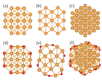
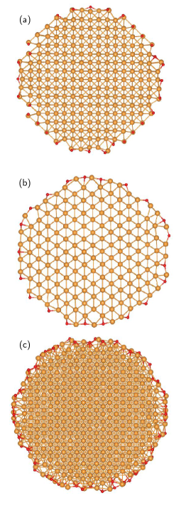
The NW structures studied in this work are based on the bulk fcc Cu structure, with [100]-, [110]- and [111]-oriented NWs chosen with approximately 1 and 3 nm diameters. Due to the small diameter of the NWs studied in this work, atoms at the NW surface will have an especially large contribution to the NW properties e.g., 57%, 59% and 49% of the atoms are at the surface for the [100], [110] and [111] 1 nm NWs, respectively. Hence in these nanostructures, electrical resistivity can be expected to be dominated by surface scattering. While standard complimentary metal oxide semiconductor (CMOS) technologies employ Ta based materials as barrier layers to prevent Cu diffusion, deposited Ta has been shown to cause diffusive scattering at the surface of thin Cu films.Chawla et al. (2011) As scaling continues, the relative contribution of surface scattering to total scattering increases dramatically and along with the barrier thickness means that Ta-based barrier layers may well become unsuitable for efficient interconnect design. To isolate barrier effects we have chosen to restrict this work to consideration of unterminated (i.e., in vacuum) and oxygen terminated (i.e., surface oxidized) NWs. The relaxed (i.e., zero strain) structures of the NWs studied are shown in Fig. 1 and Fig. 2.
Density functional theory (DFT) as implemented in the OpenMX software package Ope is used to study the electronic properties of the 1 nm diameter Cu NWs. The PBEPerdew et al. (1996) formulation of the generalized gradient approximation (GGA) exchange and correlation functional is used in conjunction with norm-conserving pseudopotentialsMorrison et al. (1993) and a strictly localized pseudo-atomic orbital (PAO) basis,Ozaki (2003); Ozaki and Kino (2004) which enables us to perform the decomposition of the transmission into localized pathways. The basis sets used are 6.0H-s4p2d2 and 7.0-s2p2 for Cu and O respectively. The first part of the basis set notation gives the PAO cutoff radius in Bohr, while the second part indicates the orbitals used for the valence electrons, e.g., O 7.0-s2p2 gives a cut-off radius of 7.0 Bohr and 8 basis functions (2 s functions and 6 p functions). This Cu basis set agrees reasonably with experiment, giving an optimal fcc lattice parameter of 3.63 Å and a bulk modulus of 135 GPa compared to experimental values of 3.615 Å and 137 GPa, respectively. The supercell approach is used and because the NWs are periodic only along their axis, a cell size incorporating a minimum of 1 nm of vacuum in the transverse directions is used such that the interaction between periodic images is minimized. The first Brillouin zone is sampled using 11 k-points generated according to the Monkhorst-Pack method Monkhorst and Pack (1976) and an energy cutoff of 200 Ry is used to generate the grid by which real space quantities are discretized. The atomic positions in the NWs are relaxed until all forces are less than 3x10⁻⁴ Hartree/Bohr; total energy is also minimized with respect to the lattice cell parameter along the NW axis for each NW orientation. Optimized lattice parameters along the NW axis are given in Table 1.
The 3 nm O-terminated NWs are also relaxed using the OpenMX software package using the same parameters. [100] and [110] NW structures are fully optimized whereas we take a hollow-core approach (described in the supporting information) for the [111] NW due to the number of atoms in the unit cell. Due to its reduced computational demand, Density Functional Tight Binding (DFTB) as implemented by the QuantumWise software packageQW ; Brandbyge et al. (2002); Soler et al. (2002) is used to calculate the electronic transport properties of the 3 nm NWs, using a density mesh cutoff of 15 Hartree and an 11 k-point Monkhorst-Pack grid. DFTB results were compared to DFT in a carefully chosen set of cases in order to explicitly assess their validity in NW structures.
The electrical properties of these NWs are modeled in the context of the Landauer-Büttiker formalism, Landauer (1957); Datta (1995) which includes the concepts of wide reflectionless contacts and electrodes. This formalism relates the electric current through a NW attached to two electron reservoirs (contacts) with the probability that an electron can be transmitted via the relation
| (1) |
where is the electron charge, Planck’s constant, is the transmission coefficient per spin channel at energy and applied bias , is the Fermi-Dirac distribution, () and () are the temperature and chemical potential of the left (right) electrode, and the applied bias is given by
| (2) |
In the case of a NW directly attached to identical electron reservoirs (i.e., same chemical potential and temperature) we may write the linear response conductance in the zero-temperature limit as
| (3) |
Given that the NW is modeled as a perfectly periodic structure, all Bloch waves propagate with unit probability. This leads to the expression for the NW contact resistance
| (4) |
where the NW acts as a ballistic waveguides for the total number of modes at the Fermi level , which includes all Bloch waves . This quantity provides information on the electrical resistivity intrinsic to the NW’s electronic structure. Throughout this work the reported transmission then corresponds to a sum over the total number of modes for each structure as a measure of their maximum potential conductivity as affected by their reduced scale and in the absence of scattering sources such as structural defects, grain boundaries, and phonons. Even though surface scattering is expected to be the most important contribution to resistance at these dimensions at zero temperature, the contribution of electron-phonon scattering at finite temperatures cannot be neglected. Plombon et al. (2006) report a decomposition of the resistance of copper lines with widths ranging from 75 to 500 nm with electron-phonon scattering estimated to account for 60% of the resistivity at 300K. The effects of electron-phonon interactions on resistivity in sub 5nm copper NWs are currently unknown and have been excluded from this study.
It is worth noting that for interconnect applications these NWs’ function would be to provide electrical contact between devices (e.g., transistors) across a short length and with small voltage drops - ideally zero. Hence the use of the linear response conductance applies and its validity can be extended to arbitrarily high temperatures as long as the transmission coefficient remains approximately constant over the energy range in which the transport takes place.
With the aim of providing some insight into the influence of the local chemical environment on electronic transport, a decomposition of transmission into spatially resolved pathways is computed according to the formalism described by Solomon et al. (2010), as implemented in the QuantumWise software package, in which the transmission through a plane perpendicular to the transport direction that divides the system in two regions and is decomposed as
| (5) |
where and are atoms on each side of said plane. We note that the use of a Green’s function implementation to the Landauer approach is required for decomposing the transmission into local contributions between pairs of atoms and hence this approach is taken for computing all electronic transport properties.
III Results and Discussion
III.1 Nanowire structure
The optimized cell parameters along the periodic direction of the NWs for a single repeat unit are given in Table 1. In the case of the unterminated NWs, the optimized cell parameter is very similar to the calculated bulk cell parameter; this agreement is reflected in the NW structures wherein the atoms move only slightly from their bulk positions after geometry optimization (see Fig. 1). When oxygen atoms are placed on the NW surface the situation changes dramatically with significant surface reconstruction seen for both the 1 nm and 3 nm NWs. There is a strong tendency for O to pull surface Cu atoms away from the NW bulk-like core until the bonded Cu and O atoms lie in a single plane. In bulk Cu(I) and Cu(II) oxide, each Cu bonds to 2 or 4 O atoms for Cu2O and CuO respectively, conversely each O atom bonds to 4 or 2 Cu atoms for Cu2O and CuO, respectively. The surface reconstruction seen in this work emulates the kinds of structural motifs seen in these oxides. The ratio of copper to oxygen (Cu:O) at the NW surface is 1.5, 1.7, and 1.9 for the 1 nm oxidized [100], [110], and [111] NWs respectively, i.e., it lies between bulk CuO and bulk Cu2O. In all cases, each O atom at the surface bonds to 3 Cu, thus the oxidation is intermediate to the situation seen for the bulk oxides. The surface oxide in the NWs consists of a very thin curved layer which locally is essentially two dimensional. Thus the NW surfaces are well oxidized as the Cu:O ratio is comparable to bulk copper oxide. For the [100] and [110] NWs, each Cu at the surface bonds to 2 oxygen atoms. Thus while the Cu:O ratio at the surfaces are different, in the case of [100] and [110] NWs, each O bonds to the same number of Cu atoms and each Cu bonds to the same number of O atoms. In spite of the similarity in the surface environment the surface geometries differ. For [100] the O-Cu-O motif is linear at Cu, while for [110] most O-Cu-O are V-shaped, a minority are linear. The [111] NW surface has 13 Cu atoms bonded each to 2 O atoms and 8 Cu atoms bonded each to 1 O atom, thus in line with the higher Cu:O ratio, this surface appears to be less oxidized than the [100] and [110] surfaces. The Cu atoms at the [111] surface which bond to two O have a mix of linear and V-shaped O-Cu-O structural arrangements.
| Unterminated | O-terminated | ||||
|---|---|---|---|---|---|
| Bulk | 1 nm | 3 nm | 1nm | 3nm | |
| [100] | 3.63 | 3.60 | 3.63 | 3.75 | 3.64 |
| [110] | 2.57 | 2.56 | 2.59 | 2.86 | 2.73 |
| [111] | 6.29 | 6.26 | - | 6.46 | - |
The surface reconstruction does not strongly affect the positions of Cu atoms below the surface layers, this is clearly evident in the 3 nm NW structures shown in Fig. 2, beyond the first two Cu surface layers the Cu atoms occupy approximately equivalent configurations with respect to their bulk positions. The reconstruction at the surface is associated with a lengthening of the optimized cell parameter relative to the bulk and unterminated NW, which is more severe for the 1 nm NWs than 3 nm NWs. This suggests that there is competition between the surface of the NW and core over the relaxed cell parameter along the axis. The oxidized surface favors an increase in length along this axis, presumably to better incorporate the surface O atoms in a layer. Conversely the core of the NW consists only of Cu atoms with their geometry similar to bulk fcc Cu and therefore favors a bulk-like cell parameter. Thus while unterminated NW cell lengths are similar for 1 and 3 nm NWs, the oxidized 3 nm NWs have a smaller (i.e., closer to the bulk value) cell parameter than the oxidized 1 nm NWs. A concomitant increase in NW diameter is not observed, therefore this change in cell parameter occurs exclusively along the NW axis. The surface structural rearrangement seen here for the O-terminated [100] NW, shown in Fig. 1(d) and Fig. 2(b), is very similar to that seen in experiment for surface oxidized Cu(100) slabsBaykara et al. (2013) suggesting the structural rearrangement we see for the NWs in our simulations is representative of experimental structures with highly prepared surface treatments.
III.2 Electron transmission
| Unterminated | O-terminated | ||||
|---|---|---|---|---|---|
| Bulk | 1 nm | 3 nm | 1nm | 3nm | |
| [100] | 28.0 | 22.8 | 19.4 | 7.3 | 8.8 |
| [110] | 29.7 | 26.7 | 24.3 | 15.3 | 15.1 |
| [111] | 27.9 | 15.3 | 11.8 | 3.7 | 4.0 |
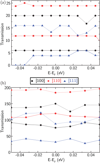
The transmission spectra calculated for the terminated and oxidized 1 nm and 3 nm Cu NWs are shown in Fig. 3 for a narrow energy range of 50 meV centered about the Fermi energy. In each case, we find that the oxidized NW has a substantially lower electron transmission than the corresponding unterminated NW. This result is consistent with the increase in resistance after chemical oxidation previously been reported by Chawla et al. (2010) for Cu thin films and arises from the reduction of the DOS at the surface upon oxidation. Additionally, we find a strong dependence of transmission on NW orientation. In all cases we find that the [110] NW has a larger transmission than [100], which in turn has a larger transmission than [111], irrespective of termination. As expected the transmission of the NWs increases going from 1 nm to 3 nm diameter due to the increasing cross-sectional area. The cross-sectional areas of the NWs are not identical as diameters deviate from exactly 1 nm and 3 nm due to the different atomic arrangements of the crystal orientations. Thus, we also calculate the transmission per unit area , presented in Table 2, to ensure that this variation in transmission with orientation is not due to deviation in cross sectional area. There is ambiguity in how to define the cross sectional area of the NWs due to atomic structure. The atoms in the NW have volume which extends beyond the nuclear positions and the smaller the NW the greater this contribution will be to the NW cross section. For simplicity we have taken the cross-section to be circular, elliptical, or octagonal as appropriate, with dimensions equal to the maximum inter-nuclear width of the NW plus twice the Cu atomic radius (1.28 Å). We find that the transmission per area follows the same trend as the total transmission plotted in Fig. 3; [110] has the largest and [111] the smallest, regardless of diameter or termination. This result is consistent with the anisotropy in Cu conductivity with crystal orientation reported recently by Hegde et al. (2014). In fact, this orientation dependence is of such significance that for the 3 nm NWs the oxidized [110] NW has a transmission comparable to the unterminated [111] NW at the Fermi energy; a remarkable result consistent with the shape of the Fermi surface of bulk fcc copper, in which the Fermi surface exhibits a vanishing DOS along the directions. The extent of the orientation dependence on transmission is also clearly evident in Table 2. In the case of unterminated NWs, the transmission for a given cross sectional area for [110] is approximately twice that of [111] NWs, after oxidation this margin further increases with the [110] transmission per unit area approximately 3.5 times larger than for the [111] NW. It may be anticipated that a more oxidized NW would show greater suppression in transmission, however the 1 nm [111] NW is in fact less oxidized than the [110] NW; each surface Cu in the [110] NW bonds to 2 oxygen atoms while surface [111] atoms bond to either 1 or 2 oxygen atoms. Meanwhile, unterminated [100] and [110] NWs show similar transmission per unit area; [100] is about 4 units smaller than [110] for both 1 nm and 3 nm NWs. After oxidation, the transmission per unit area for [100] NWs is approximately 60% of [110] NWs, i.e., transmission suppression on oxidation is relatively larger for [100] than [110]. Thus both the surface chemical environment and the NW orientation play a critical role in determining the overall transmission of the copper NW.
III.3 Local transmission paths
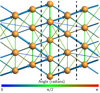
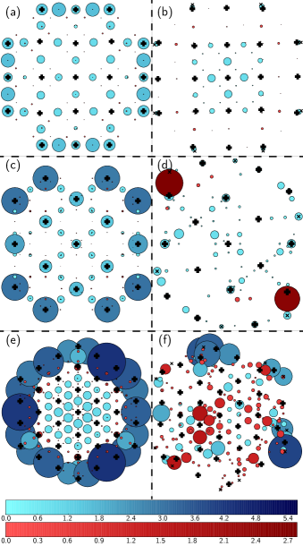
The transmission results show that orientation and surface environment drastically impact on Cu NW electron transport. These effects are not easy to decouple, however, a greater understanding of the relationship between them can be established by examining transmission through the NW at an atomic scale. We have calculated transmission pathways in the NWsSolomon et al. (2010) at the Fermi level, which are shown in Fig. 4 for the unterminated [111] NW, to particularly elucidate the effects of NW crystal orientation and surface oxidation on transmission. Transmission pathways provide a visual representation of transmission through the NW with the arrow width representing the size of the transmission between an atom pair. As described in the caption of Fig. 4, the arrows are colored according to their angle with respect to the NW axis; blue arrows correspond to forward transmission, green arrows to radial transmission (i.e., atoms within the same transverse plane), and red arrows backscattering or reflection. As expressed in Eq. (5), the transmission pathways crossing a given plane perpendicular to the transport direction always sum to give the total transmission coefficient.
A more convenient visual representation is portrayed in Fig. 5 in which the intersections of transmission pathways with planes located halfway between non-equivalent atomic planes give a clear image of the decomposition of the total transmission into pathways per cross-sectional area per NW. Such planes are indicated by dashed black lines in Fig. 4 for the case of the unterminated [111] NW. These projections provide a heuristic representation of localized transmission and allow quick identification of where the most important contributions lie within the NW cross-section.
Fig. 5(a) shows transmission pathways for the unterminated [100] NW. There are transmission pathways both parallel (’dots’ centered at atomic positions) and angled to the NW axis (centered between atomic positions). Angled pathways are larger in magnitude than parallel pathways as represented by their larger ’dot’ diameter and their color. This difference in magnitude can be attributed to the distance between the Cu atoms being larger if a direct route parallel to the axis is taken (3.60 Å versus 2.53 Å). It is is readily seen that pathways along the surface dominate electron transmission for this NW as the ’dots’ in the surface are larger than below the surface, where the parallel pathways are smaller and obscured by the symbols indicating the atomic positions.
The unterminated [110] NW transmission pathways are shown in Fig. 5(c). Transmission involving only surface atoms occurs along the NW axis and is large (indicated by the darker blue ’dots’ centered about atomic positions) while pathways at an angle to the axis exhibit much lower transmission. Below the surface the situation is similar, transmission along the axis is larger than off-axis. In this orientation the Cu atom separation is similar for both parallel and off axis transmission and thus the more direct parallel route is favored. As for the unterminated [100] NW, transmission is larger at the NW surface than below the surface with the largest ’dots’ corresponding to pathways located at the surface and parallel to the NW axis. The transmission pathways for the unterminated [111] NW, shown in Fig. 5(e). In this case, there is no significant transmission directly parallel to the NW axis, this is presumably because the Cu interatomic distance along the NW axis is simply too large compared to the off axis distances (6.26 Å versus 2.5 Å reflecting that no nearest neighbors align along the NW axis). As previously mentioned, this result is consistent with the vanishing density of states found along the directions in the Fermi surface of fcc Cu; there are no transmission paths parallel to the [111] direction as shown by the absence of arrows parallel to the NW axis in Fig. 4 and of ’dots’ centered about atomic positions in Fig. 5(e). As shown in Fig. 4 transmission pathways tend to flow along the NW surface until they reach a Cu atom with a low coordination number (such as the one at the top center of the figure), at which point the electrons are scattered into the NW core where they continue to propagate along angled paths until they reach another surface where this process repeats. The lack of transmission pathways parallel to the [111] NW axis makes the surface critical as all paths inevitably lead to the surface. While there are some transmission pathways inside the core of the NW, transmission through the NW occurs primarily at the NW surface; and much like the unterminated [100] and [110] NWs, transmission is larger at the surface. However, in this case as well as ’dots’ representing forward transmission, the ’dots’ representing negative values (i.e., electron backscattering or reflection paths) are much larger than for the unterminated [100] and [110] NWs.
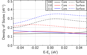
The transmission pathways of the unterminated NWs consistently show that transmission is larger at the NW surface than in the core and also that backscattering for these NWs is relatively small, particularly for the [100] and [110] NWs in which the total magnitude of all reflecting paths is 14% and 13% of that of forward paths, whereas for [111] NWs this value increases to 25%. This surface-dominated transmission can be explained in terms of the increased local density of states (LDOS) of surface atoms at the Fermi level as a result of their low coordination. This allows electrons otherwise localized at bonds to become available for transmission at the surface atoms. Fig. 6 shows the average local density of states (LDOS) of an atom situated at the surface and of an atom close to the center of the NWs’ cross section; the atoms at the surface show a larger density of states in the range around the Fermi level studied in this work. Unterminated [111] NWs exhibit the largest boost with the average LDOS value of a surface atom being 2.55 times that of an atom near the center of the NW at the Fermi level; similarly, atoms at the surface of [100] NWs have an average surface-to-center LDOS ratio of 2.41 and a considerably lower ratio of 1.39 is found for [110] NWs.
As might be expected from the transmission spectra shown in Fig. 3 and the previous analysis, oxidation of the NWs changes the behavior at the NW surfaces considerably. In the [100] NW, transmission at and just below the NW surface is reduced upon oxidation, in fact Fig. 5(b) shows that near the surface forward transmission is largely suppressed and backscattering pathways are enhanced. In the core of the NW the transmission is similar to the unterminated NW as shown by similarly arranged, sized and colored ’dots’. Thus in the case of the [100] NW, oxidation appears to affect the surface and immediate subsurface almost exclusively. In the case of the [110] NW, more significant back scattering is seen upon surface oxidation with the appearance of the large red ’dots’ indicating a relatively large magnitude in Fig. 5(d). Unlike the [100] NW, transmission is also reduced in the core of the [110] NW upon surface oxidation. A suppression of the pathways parallel to the NW axis can be clearly seen all the way to the center when comparing to the unterminated NW (5)(c). Thus it appears that the effect of surface oxidation is felt deeper in the NW for the [110] orientation compared to [100]. However, transmission per unit area for the oxidized [100] NW actually drops more relative to the unterminated NW compared to the [110] orientation, as reported in Table 2. This is likely caused by a reduction of transmission at the surface and immediate subsurface in the [100] oxidized NW, in which the surface has a larger contribution relative to the core in the unterminated case as shown in Fig. 6 and discussed above. The surface of the oxidized [111] NW is more disordered than the oxidized [100] and [110] NWs studied in this work. This disorder along with the indirect transmission associated with transport along this crystal orientation leads to a complicated, disordered transmission pathways (Fig. 4(f)) consistent with the low transmission calculated for this structure. In contrast to the [100] and [110] oxidized NWs, there is large forward transmission at the surface for the oxidized [111] NW, which can be seen clearly in the mapping of the transmission pathways onto a cross sectional area of the [111] NW shown in Fig. 5(f). However, the large backscattering paths in the core of the NW result in a lower overall transmission; all paths in the core lead either to the surface (where oxidation has largely suppressed forward transmission) or are backscattered.
III.4 Transmission model
To understand the behavior of the total transmission per NW given in the previous sections, we provide an analysis for a simple model describing the electron transmission behavior of round NWs which partitions the NWs into regions of similar behavior based on the magnitudes of the transmission pathways within the them. The generalization of the model to other geometries is straightforward. The model provides insight into the observation that transmission per unit area decreases as area increases for the unterminated NWs and that the transmission per unit area is relatively constant for oxidized NWs for a given orientation.
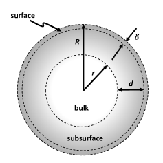
The total transmission of a round NW of radius is divided into contributions from three distinct regions of the NW; the surface, the subsurface and the bulk regions; as shown in Fig. 7 for a cross section of the NW. The surface region is described by a thickness , the subsurface region by a thickness and the bulk-like core is described by a radius ; therefore
| (6) |
To each region is assigned a transmission per unit area . The surface transmission per unit area is assumed constant, whereas the subsurface transmission per unit area can vary with depth into the NW as signified by the grading in Fig. 7. However, it is assumed that an effective transmission per unit area can be assigned to the subsurface region. The bulk region is defined as the core atoms for which the transmission per unit area approaches the bulk behavior .
The area of the surface region can be expressed as
| (7) |
which for can be approximated as
| (8) |
Similarly the area for the subsurface region can be expressed as
| (9) |
which for is given as
| (10) |
The core region displaying bulk-like behavior has an area given by
| (11) |
which for becomes
| (12) |
The fact that and scale linearly with whereas scales as for large values of simply describes the fact that the surface and subsurface play decreasing roles as the NW’s radius is increased. An effective transmission per unit area is then defined for each region and the total transmission is expressed as
| (13) |
To explore the role of the surface and subsurface transmission per unit area in small cross section NWs we consider four cases.
Case I: . In this limit, the surface dominates and transport is given purely by the surface and represents, for example, the case of an atomic chain.
Case II: . This condition describes when the cross sectional area of the NW is of a scale that a subsurface region is present but the NW diameter is not large enough for the core of the NW to display bulk behavior for transmission (it should be noted that the subsurface region is not sharply defined as represented by the grading of the gray region used to define it in Fig. 7). In the transmission plots of Fig. 5 for the unterminated Cu NWs, it can be seen that the subsurface region has a lower transmission per unit area compared to the NW surface regions. Hence by decreasing the NW diameter from 3 nm to 1 nm, a larger transmission per unit area is obtained consistent with the results listed in Table 2.
Case III: . As the NW radius increases, eventually a core region is formed whereby local transmission pathways approach the values obtained in bulk copper. When this core region is of a comparable dimension to the surface and subsurface layer, the transmission per unit area will reflect the contributions from the different regions. As the subsurface region in unterminated Cu NWs has a lower transmission per unit area than the bulk, the overall transmission per unit area will increase relative to Case II as the region forms.
Case IV: . As the NW’s radius is further increased, the core region’s contribution will quickly dominate due to the area increasing as as opposed to the linear dependence on NW radius for the surface and subsurface regions. Hence the transmission per unit area for the NW will increase with increasing until asymptotically approaching the bulk value.
The following picture emerges in the case of unterminated NWs. For extremely small diameter NWs with diameters of approximately 1 nm, surface and subsurface transmissions combine to provide a transmission per unit area that is comparable to bulk copper for [100] and [110] and less than bulk copper for [111]. As the NW diameter increased, for example up to 3 nm, the lower subsurface transmission with respect to surface transmission results in a net lowering of overall transmission per unit area compared to smaller diameter NWs. As the NW diameter is increased further, the core region begins to behave like a bulk conductor and the transmission rises and asymptotically approaches the bulk transmission per unit area.
The picture needs to be slightly modified for the case of NWs with surface oxidation. As seen in Fig. 5, the surface transmission is reduced significantly due to surface oxidation. From Table 2, it is seen that the transmission per unit area for the 1 nm and 3 nm diameter NWs are comparable. Once oxidized, the transmission at the surface is suppressed and the transmission of the subsurface region dominates. We anticipate that the transmission per unit area of the subsurface region for a given orientation is similar for 1 nm and 3 nm NWs and this combined with the low surface transmission (see Fig. 5) leads to the transmission per unit area for each orientation being approximately constant going from 1 nm to 3 nm diameter, as reported in Table 2. However, the transmissions of both 1 nm and 3 nm oxidized NWs are much lower than found for the bulk, and hence larger cross section NWs are required before significant bulk-like behavior from the core contributes to the net transmission per unit area.
IV Conclusion
The electron transport properties of 1 nm and 3 nm diameter copper NWs have been calculated in each case for unterminated and surface oxidized NWs of [100], [110] and [111] crystal orientations. We find even 1 nm diameter copper NWs to be metallic, however electron transmission is strongly dependent on both surface termination and crystal orientation. Surface oxidation suppresses electron transmission compared to unterminated copper NWs, consistent with previous reports for copper thin films. The [110] oriented NWs consistently show a higher electron transmission than [100] oriented NWs which in turn have a higher electron transmission than [111] NWs. Transmission in unterminated copper NWs is larger at the NW surface than below the surface, irrespective of crystal orientation. A different picture emerges for surface oxidized NWs wherein transmission is lower at the NW surface than in the subsurface for [100] and [110] oriented NWs. However while the oxidized [111] NW surface transmission is reduced compared to the unterminated NW, it nonetheless continues to show larger surface transmission than subsurface transmission. Transmission per unit area decreases with increasing diameter for unterminated NWs but remains approximately constant for the surface oxidized NWs studied. A simple model of transmission in round NWs which divides the NW into regions based on local transmission pathways explains the differing behaviors of unterminated and oxidized NWs. Briefly, transmission per unit area is lower in the subsurface region than at the surface for the unterminated NWs studied, thus when the diameter is increased from 1 nm to 3 nm the transmission per unit area of the NW decreases as the subsurface region becomes relatively more important. In oxidized NWs, the overall transmission per unit area is comparable for 1 nm and 3 nm NWs. The suppression of the surface transmission in this case increases the contribution of the subsurface to overall transmission and a similar subsurface transmission per unit area may be expected for 1 nm and 3 nm oxidized NWs for the same crystal orientation resulting in similar overall transmission per unit area. Overall, our results suggest that conductivity in sub 3 nm copper NWs is highly sensitive to crystal orientation and surface termination, and that careful material preparation and processing will be essential in order to maximize conductivity.
Acknowledgements.
This work was performed as part of the Intel-Tyndall research collaboration sponsored by Intel Components Research. ASS was funded under an Irish Research Council postgraduate scholarship. We are grateful to QuantumWise A/S for providing access to the QuantumWise simulation software.References
- (1) http://www.itrs.net/reports.html .
- Steinhögl et al. (2002) W. Steinhögl, G. Schindler, G. Steinlesberger, and M. Engelhardt, Phys. Rev. B 66, 075414 (2002).
- Zhang et al. (2007) W. Zhang, S. H. Brongersma, Z. Li, D. Li, O. Richard, and K. Maex, Journal of Applied Physics 101, 063703 (2007).
- Fuchs (1938) K. Fuchs, Mathematical Proceedings of the Cambridge Philosophical Society 34, 100 (1938).
- Mayadas and Shatzkes (1970) A. F. Mayadas and M. Shatzkes, Phys. Rev. B 1, 1382 (1970).
- Plombon et al. (2006) J. J. Plombon, E. Andideh, V. M. Dubin, and J. Maiz, Applied Physics Letters 89, 113124 (2006).
- Josell et al. (2009) D. Josell, S. H. Brongersma, and Z. Tokei, Annual Review of Materials Research Annual Review of Materials Research, 39, 231 (2009).
- Henriquez et al. (2010) R. Henriquez, S. Cancino, A. Espinosa, M. Flores, T. Hoffmann, G. Kremer, J. G. Lisoni, L. Moraga, R. Morales, S. Oyarzun, M. A. Suarez, A. Zúñiga, and R. C. Munoz, Phys. Rev. B 82, 113409 (2010).
- Henriquez et al. (2013) R. Henriquez, M. Flores, L. Moraga, G. Kremer, C. González-Fuentes, and R. C. Munoz, Applied Surface Science 273, 315 (2013).
- Sun et al. (2009) T. Sun, B. Yao, A. P. Warren, K. Barmak, M. F. Toney, R. E. Peale, and K. R. Coffey, Phys. Rev. B 79, 041402 (2009).
- Sun et al. (2010) T. Sun, B. Yao, A. P. Warren, K. Barmak, M. F. Toney, R. E. Peale, and K. R. Coffey, Phys. Rev. B 81, 155454 (2010).
- Graham et al. (2010) R. L. Graham, G. B. Alers, T. Mountsier, N. Shamma, S. Dhuey, S. Cabrini, R. H. Geiss, D. T. Read, and S. Peddeti, Applied Physics Letters 96, 042116 (2010).
- Wang et al. (2012) P.-I. Wang, M. D. Frey, M. Washington, S. Nayak, and T.-M. Lu, Thin Solid Films 520, 6106 (2012).
- Chawla and Gall (2009) J. S. Chawla and D. Gall, Applied Physics Letters 94, 252101 (2009).
- Chawla et al. (2010) J. S. Chawla, F. Zahid, H. Guo, and D. Gall, Applied Physics Letters 97, 132106 (2010).
- Chawla et al. (2011) J. S. Chawla, F. Gstrein, K. P. O’Brien, J. S. Clarke, and D. Gall, Phys. Rev. B 84, 235423 (2011).
- Zahid et al. (2010) F. Zahid, Y. Ke, D. Gall, and H. Guo, Physical Review B 81, 045406 (2010).
- Hegde et al. (2014) G. Hegde, M. Povolotskyi, T. Kubis, J. Charles, and G. Klimeck, Journal of Applied Physics 115, 123704 (2014).
- Solomon et al. (2010) G. Solomon, C. Herrmann, T. Hansen, V. Mujica, and M. Ratner, Nature Chemistry 2, 223 (2010).
- (20) www.openmx-square.org .
- Perdew et al. (1996) J. Perdew, K. Burke, and M. Ernzerhof, Physical Review Letters 77, 3865 (1996).
- Morrison et al. (1993) I. Morrison, D. Bylander, and L. Kleinman, Physical Review B 47, 6728 (1993).
- Ozaki (2003) T. Ozaki, Physical Review B 67, 155108 (2003).
- Ozaki and Kino (2004) T. Ozaki and H. Kino, Physical Review B 69, 195113 (2004).
- Monkhorst and Pack (1976) H. J. Monkhorst and J. D. Pack, Phys. Rev. B 13, 5188 (1976).
- (26) Atomistix ToolKit version 2014-1 QuantumWise A/S (www.quantumwise.com) .
- Brandbyge et al. (2002) M. Brandbyge, J.-L. Mozos, P. Ordejón, J. Taylor, and K. Stokbro, Phys. Rev. B 65, 165401 (2002).
- Soler et al. (2002) J. M. Soler, E. Artacho, J. D. Gale, A. García, J. Junquera, P. Ordejón, and D. Sánchez-Portal, Journal of Physics: Condensed Matter 14, 2745 (2002).
- Landauer (1957) R. Landauer, IBM Journal of Research and Development 1, 223 (1957).
- Datta (1995) S. Datta, Electronic Transport in Mesoscopic Systems (Cambridge University Press, 1995).
- Baykara et al. (2013) M. Z. Baykara, M. Todorovifi, H. Mönig, T. C. Schwendemann, O. Ünverdi, L. Rodrigo, E. I. Altman, R. Pérez, and U. D. Schwarz, Phys. Rev. B 87, 155414 (2013).