STEM: A Scheme for Two-phase
Evaluation of Majority Logic
Abstract
The switching time of a magnet in a spin current based majority gate depends on the input vector combination, and this often restricts the speed of majority-based circuits. To address this issue, this work proposes a novel two-phase scheme to implement majority logic and evaluates it on an all-spin logic (ASL) majority-based logic structures. In Phase 1, the output is initialized to a preset value. Next in Phase 2, the inputs are evaluated to switch the output magnet to its correct value. The time window for the output to switch in Phase 2 is fixed. Using such a scheme, an -input AND gate which requires a total of () inputs in the conventional implementation can now be implemented with only () inputs. When applied to standard logic functions, it is demonstrated that the proposed method of designing ASL gates are 1.6–3.4 faster and 1.9–6.9 more energy-efficient than the conventional method, and for a five-magnet full adder, it is shown that the proposed ASL implementation is 1.5 faster, 2.2 more energy-efficient, and provides a 16% improvement in area.
Index Terms:
Spintronics, All-spin logic, Majority logic, Two-phase logic.I Introduction
Spintronics is widely viewed as a promising technology for the post-CMOS era [1]. Several new concepts for implementing logic functions using spin-based devices have been proposed in this regard, including quantum cellular automata (QCA) [2, 3, 4], all-spin logic (ASL) [5], charge spin logic [6], and magnetoelectric-based logic [7, 8]. The fundamental logic building blocks implemented with these devices are based on the majority logic paradigm, where the input states compete with each other and the majority prevails as the output logic state. In this work, we propose a scheme that speeds up the implementation of majority-logic-based devices using a two-phase method, and we demonstrate this idea with the help of ASL gates.
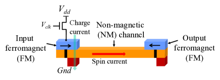
The simplest ASL gate is an inverter [9], shown in Fig. 1, which consists of a ferromagnet at the input and another at the output, with a non-magnetic channel between the two. An applied voltage on the input magnet results in electron flow due to charge current from to . The input magnet polarizes the charge current and generates a spin current. The spins that align with the direction of the magnetization pass through the magnet and those that are opposite to it are reflected onto the channel. This creates an accumulation of electron spins at the start of the channel beneath the input magnet. These spins then diffuse through the spin channel to the output end and switch the output magnet using spin torque transfer (STT) mechanism. The structure of a buffer is similar to that of an inverter, but it uses an applied voltage of at the input end instead.
In a conventional ASL majority (MAJ) gate [5], input magnets are used to inject spin currents that are sent along a channel. The spin currents from each of the input magnets compete, and the net spin current that reaches the output end is an algebraic sum of the spin current from each input magnet to the output. The delay is a function of the input vector combination. Combinations where all inputs assume the same logic value inject noncompeting spin currents. For these cases, the net current at the output is larger, and hence the delay is lower than cases where some spin current contributions cancel others. We propose an alternative logic implementation that exploits the timing difference between the evaluation of the output for various logic states. We refer to our approach as STEM, a Scheme for Two-phase Evaluation of Majority logic. Under this scheme, the output magnet is initialized to a predefined logic stage in the first phase; in the second phase, currents from a subset of input magnets compete to evaluate the output to its correct logical value.
Two-phase schemes have been used in the past in the context of majority logic. For QCA [10, 11], the first phase pulls the quantum nanodots from “null” state to “active” state by altering their energy profile, while the second phase evaluates the output logic state through the interaction with neighboring quantum nanodots. Recent work in [12] uses a two-phase scheme for ASL logic, where a bias voltage applied to the magnets in the first stage orients the magnetization along the hard axis, and the output is evaluated in the second stage to switch the output magnet to the correct state. In short, all of these approaches initialize the system to a state between the logic 0 and logic 1 states so that part of the transition is completed during the first phase. In contrast, we do not attempt to place the gate in such an intermediate state, which can sometimes be unstable. Furthermore, unlike these prior approaches, our work explicitly leverages the delay dependence of the logic gate on the input vector to develop faster and more energy-efficient logic.
The remainder of the paper is organized as follows. In Section II, we describe the conventional implementation of majority logic in ASL and how such an implementation can be used to build (N)AND/(N)OR gates. Next, an overview of STEM is provided in Section III, followed by a more detailed discussion of its circuit-level implementation in Section IV. A detailed performance model, described in Section V, is then used to apply STEM on a set of standard logic functions and a full adder in Section VI. Finally, concluding remarks are presented in Section VII.
II Conventional majority logic implementations
In this section, we first demonstrate the basics of the majority logic function used to implement spin-based majority gates or AND/OR/NAND/NOR gates, and then show that this structure can result in large disparities in the delay, depending on the input vector combination. Due to this disparity, in many cases the circuit may be active for an unnecessarily long time, sinking power.
II-A The majority logic function
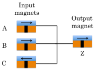
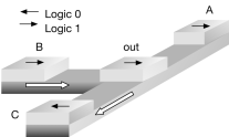
The majority logic function, MAJ operates on a set of binary logic inputs and outputs the value that represents the majority. For an odd number of inputs, the output is always binary. A three-input majority logic function, MAJ3(A,B,C), operates on Boolean inputs A, B, and C to produce an output Z, as illustrated in Fig. 2. The corresponding truth table in Fig. 2 illustrates the notion that the signal that propagates to the output is 3 stronger when all inputs are identical as compared to the other cases, and to a first order, this translates to a 3 faster switching speed for the stronger signal.
| A | B | C | Z | Strength |
|---|---|---|---|---|
| 1/Delay | ||||
| 0 | 0 | 0 | 0 | 3 |
| 0 | 0 | 1 | 0 | 1 |
| 0 | 1 | 0 | 0 | 1 |
| 0 | 1 | 1 | 1 | 1 |
| 1 | 0 | 0 | 0 | 1 |
| 1 | 0 | 1 | 1 | 1 |
| 1 | 1 | 0 | 1 | 1 |
| 1 | 1 | 1 | 1 | 3 |
| A | B | C | Z | Strength | ||
|---|---|---|---|---|---|---|
| 1/Delay | ||||||
| 0 | 0 | 0 | 0 | 0 | 0 | 5 |
| 0 | 0 | 1 | 0 | 0 | 0 | 3 |
| 0 | 1 | 0 | 0 | 0 | 0 | 3 |
| 0 | 1 | 1 | 0 | 0 | 0 | 1 |
| 1 | 0 | 0 | 0 | 0 | 0 | 3 |
| 1 | 0 | 1 | 0 | 0 | 0 | 1 |
| 1 | 1 | 0 | 0 | 0 | 0 | 1 |
| 1 | 1 | 1 | 0 | 0 | 1 | 1 |
II-B Realizing AND/OR gates using majority logic
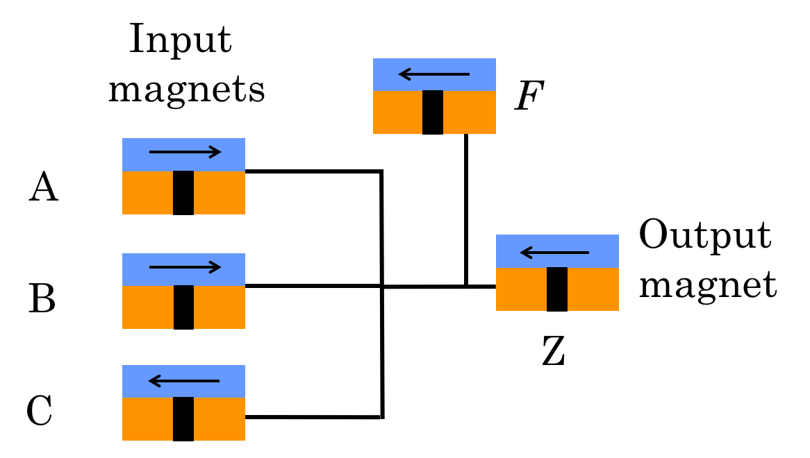
In prior work, techniques for implementing -input gates that realize AND, OR, NAND, and NOR functionalities based on majority logic primitives have been proposed [9]. An -input AND gate, illustrated in Fig. 3 for , is realized using a majority gate with inputs, which include the inputs of the AND gate and fixed inputs at logic 0. The majority function achieves a value of 0 only when all inputs to the AND gate are at logic 1. Similarly, an -input OR gate augments the inputs with fixed inputs at logic 1. The implementation of NAND and NOR gates requires an inversion after the AND and OR functionalities, respectively, and in some technologies, this inversion can be applied inexpensively. For instance, as indicated in Section I, an ASL implementation simply requires an inversion of the and polarities for the gate.
Fig. 3 illustrates the net signal strength associated with the majority function evaluation for an AND3 gate using a MAJ5 structure. Since the strength of the signal can vary by 5 over all inputs, this implies that the gate delay can be 5 faster for the 000 case, as compared to the 011, 101, 110, and 111 inputs.
III STEM: A two-phase majority logic scheme
In this section, we will describe an alternative implementation of the gates described above. The method proceeds in two phases:
-
•
Phase 1: Initialization: The output is initialized to a specific value.
-
•
Phase 2: Evaluation: The gate inputs are applied to potentially update the output, but the evaluation step is terminated at time .
This method is superficially similar to the idea of domino logic in CMOS circuits, where the output is initially precharged to logic 1, and then evaluated and conditionally discharged. However, in domino logic, the initialization phase typically corresponds to a precharge that sets the output to logic 1, which is conditionally discharged during the evaluation phase; as we will see, the approach used here is different.
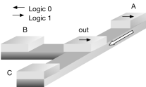
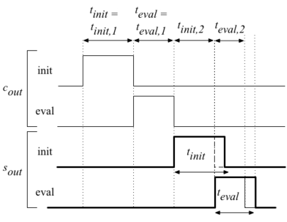
We demonstrate our idea on an implementation of the majority function, MAJ3(A,B,C). In the initialization phase the output is set to the value of one of the inputs, say A, as shown in Fig. 4. During the evaluation phase, the other two inputs are applied to a two-input majority gate that drives the output, as illustrated in Fig. 4. If the two inputs are the same, they clearly form a majority and overwrite the output. If they are unequal, then they leave the initialization undisturbed, again resulting in the correct output. Note that the only case in which the logic is switched is when the inputs B and C both disagree with input A, and the switching time is , based on the assumptions in Fig. 3.
In the conventional scheme, the magnets corresponding to A, B, and C must be symmetric and must contribute an equal spin current. However, in our scheme, the precharging magnet, corresponding to A above, could be arbitrarily strong and could potentially perform precharge very quickly. The other magnets, corresponding to B and C in our example, must be symmetric and could be smaller, to achieve a better power-delay tradeoff.
| A | B | C | Output | Output |
|---|---|---|---|---|
| (Phase 1) | (Phase 2) | |||
| 0 | 0 | 0 | 0 | 0 |
| 0 | 0 | 1 | 0 | 0 |
| 0 | 1 | 0 | 0 | 0 |
| 0 | 1 | 1 | 0 | 1 |
| 1 | 0 | 0 | 1 | 0 |
| 1 | 0 | 1 | 1 | 1 |
| 1 | 1 | 0 | 1 | 1 |
| 1 | 1 | 1 | 1 | 1 |
An AND2 gate is implemented in majority logic as a MAJ3 gate with one input set to logic 0: this idea can therefore be used above. In this case, the constant logic 0 input can be used in the precharge phase, so that precharge could proceed in parallel with computing the values of the inputs to the AND2 gate, which may come from a prior logic stage.
For an AND gate with a larger number of inputs, such as an AND3 gate, a similar idea may be used, but now an evaluation deadline is introduced. For the AND3 gate, for all eight input combinations for such a gate, the results at the end of Phases 1 and 2 are shown in Table II. Note that while several combinations (011, 101, and 110) would normally evaluate to a majority value of logic 1, the net spin current, shown in the table, is weaker than the 111 case, implying that the amount of time required to change the state of the output magnet is about . This large gap not only provides fast evaluation, but also provides a safe margin beyond , so that it is unlikely that marginally early evaluations of the 011, 101, or 110 case (e.g., due to process variations) will corrupt the output value.
The advantage of using the STEM technique is threefold:
-
1.
As pointed out above, STEM can improve gate delays.
-
2.
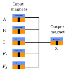
STEM often requires fewer magnets to implement various gate structures, implying that the gate area is reduced. For example, for the -input AND gate, a single fixed input magnet (Fig. 5) can initialize the output magnet to logic state in Phase 1, as against the fixed inputs required for the conventional ASL implementation, resulting in a savings of magnets.
-
3.
For AND gates implemented using STEM, this reduction in the number of input magnets reduces the number of spin currents that are sent to compete at the output, and thus directly results in a more energy-efficient implementation.
| A | B | C | Output | Net spin | Output |
|---|---|---|---|---|---|
| (Phase 1) | current | (Phase 2) | |||
| 0 | 0 | 0 | 0 | 0 | |
| 0 | 0 | 1 | 0 | 0 | |
| 0 | 1 | 0 | 0 | 0 | |
| 0 | 1 | 1 | 0 | 0 | |
| 1 | 0 | 0 | 0 | 0 | |
| 1 | 0 | 1 | 0 | 0 | |
| 1 | 1 | 0 | 0 | 0 | |
| 1 | 1 | 1 | 0 | 1 |
IV Applying this scheme at the circuit level
IV-A Gate-level control signals
The previous section presented an outline of the two-phase STEM scheme. We now concretely show the use of clocking signals at the gate level that enable the deployment of this scheme, ensuring that the initialization and evaluation phases are correctly scheduled.
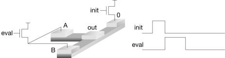
We show the example of an AND2 gate in Fig. 6. First, the “init” signal is activated during the initialization phase to transmit data from the fixed-zero input to the output magnet. After initialization is completed, the evaluation phase, enabled by the “eval” signal, is activated to alter the initialized output value, if necessary. Note that for an AND2 gate, the length of the “eval” pulse is unconstrained, but for other types of gates, such as the AND3 gate described in Table II, the minimum and maximum pulse width are both constrained: under the coarse delay model proposed earlier, the minimum width of the signal is , and the maximum width is .
IV-B A simple example
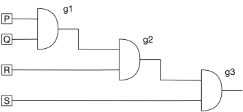
Consider the circuit shown in Fig. 7, consisting of three AND2 gates. The evaluation of the three gates proceeds along the schedule shown in Fig. 8, as follows:
-
•
We assume that the input magnets connected to the primary inputs P, Q, R, and S are initialized when the computation starts.
-
•
When the computation begins, the gate at the first level, g1, is initialized.
-
•
After initialization is complete, the gate is evaluated, and simultaneously, gate g2 is initialized.
-
•
In the next time step, g2 is evaluated and g3 is initialized, and finally, g3 is evaluated.
Note that when the next level of logic is a (N)AND or (N)OR gate, its initialized value is a constant. Therefore, for such scenarios, it is possible to simultaneously initialize the next level of logic in parallel with the evaluation of the current level. For a majority gate, such simultaneous initialization is not possible, as we will see in the next subsection.
The timing of these signals is detailed in Fig. 8. We denote the widths of the initialization and evaluation pulses for each gate by and , respectively. For this simple example, all gates are identical and therefore have the same value of and the same value of ; however, in general, . The clocking complexity for the “init” and “eval” signals is comparable to that of CMOS domino logic, and similar methods can be used for generating these clock signals globally and distributing them.
Clearly, the time required to evaluate each gate is . Since for g2 overlaps with for g1, the initialization of g2 can occur immediately after g1 is evaluated. Similarly, the evaluation pulse to g3 is applied units after the evaluate pulse to g2 is applied. The same logic can be applied to say that the evaluation pulses to successive stages must also be delayed by time .
| time | g1 | g2 | g3 |
|---|---|---|---|
| 0 | init | – | – |
| eval | init | – | |
| – | eval | init | |
| – | – | eval |
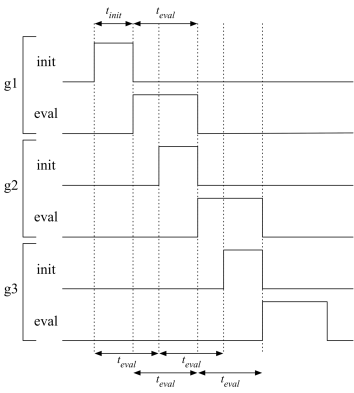
Further, it can be seen that the total evaluation time for this structure (or any structure with only (N)AND/(N)OR gates) is , implying that the initialization cost must be paid just once for the first gate, and the evaluation cost dominates for long chains of gates. Note also as observed in Section III, the initialization can generally be made much faster than evaluation. This can be done since the size of the initializing magnet can be made much larger than the others and can also be placed closer to the output magnet as there is no need for symmetry with the other magnets, as in the conventional implementation.
IV-C The five-magnet adder
The implementation of majority logic allows a spintronic full adder to be implemented using five magnets [13, 14], as shown in Fig. 9. We will refer to the corresponding ASL circuit as the conventional implementation. In this section, we show that we can achieve a faster full adder implementation with STEM using the same number of magnets.

| Strength | ||||||
|---|---|---|---|---|---|---|
| 0 | 0 | 0 | 0 | 1 | 3 | 0 |
| 0 | 0 | 1 | 0 | 1 | 1 | 1 |
| 0 | 1 | 0 | 0 | 1 | 1 | 1 |
| 0 | 1 | 1 | 1 | 0 | 1 | 0 |
| 1 | 0 | 0 | 0 | 1 | 1 | 1 |
| 1 | 0 | 1 | 1 | 0 | 1 | 0 |
| 1 | 1 | 0 | 1 | 0 | 1 | 0 |
| 1 | 1 | 1 | 1 | 0 | 3 | 1 |
The principle of the conventional five-magnet adder is that it operates in two stages. In the first stage, the value of the output carry, , is computed using the function MAJ3(,,). In the second stage, the value of the sum, , is calculated as MAJ5(,,,,). In the conventional implementation, the delay of the full adder is the sum of the delay of MAJ3 gate to calculate in the first stage and the delay of MAJ5 gate to calculate . Both MAJ3 and MAJ5 gate are implemented using conventional ASL. The results of this computation are as shown in columns 4 and 7 of Fig. 10. The layout of this adder is shown in Fig. 11(a).
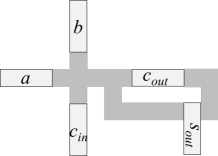
(a) (b)
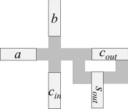
The STEM-based full adder, whose layout is shown in Fig. 11(b), modifies the above scheme and is implemented as described below. As in the conventional adder, the first stage of logic computes as MAJ3(,,), but in this case, the MAJ3 gate is built using STEM, as explained in Section II-A. To implement the STEM MAJ5 structure, we observe that the original circuit is similar to the structure in Fig. 3, except that the fixed magnets carry the value of . This indicates that a two-phase STEM structure similar to Fig. 5, but with modified initialization, can be used to implement MAJ5.
The sequence of operations, illustrated in Fig. 12, is:
-
1.
In MAJ3 Phase 1, input is first used to initialize by applying an “init” signal to magnet .
-
2.
In MAJ3 Phase 2, the “eval” signal is activated on inputs and and their value is used to evaluate and potentially update the magnet.
-
3.
Since the signal acts as the initializing signal for , the “init” signal that effects this transfer can only be applied after has been computed. Note that this implies that unlike the AND gate example previously described, there is no overlap with the evaluation phase of the previous stage.
-
4.
Finally, in MAJ5 Phase 2, we compute MAJ3(,,) and use the resulting spin current to attempt to update the magnet. Note that the lengths of the paths from each of these three input magnets to are balanced to ensure equal contributions for the MAJ3 function.
The evaluation times for MAJ3 and MAJ5 are denoted as and , respectively and will typically be different. As we will show in Section VI-C, the timing signals and their sequence can be optimized to reduce the number of global clock signals, but for this clocking scheme, let the time required to initialize in the first step and in the third step be denoted as and , respectively. The circuit delay is then given by .
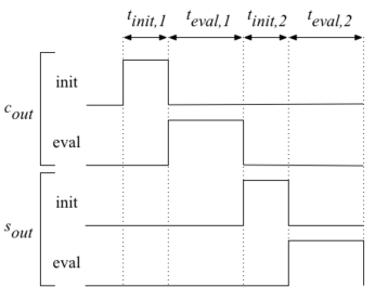
The timing requirements for the fourth step, MAJ5 Phase 2 are similar to those for the structure in Fig. 5, where we allow a limited time to perform the update. In particular, this time is chosen such that a 3 current strength (corresponding to the 000 or 111 combinations) can write the magnet, but any of the other input combinations (which all correspond to 1 current strengths) do not have sufficient time to switch the output magnet. This places both an upper and lower bound on , the time required to implement MAJ5 Phase 2, but in practice the large gap between the delay for a 1 vs. 3 current implies that the upper bound is not a significant factor. For the adder that is evaluated in Section VI using precise timing models, the 1 signal is found to be 2.7 more than , while the value of is similar to that of .
The STEM-based full adder above uses to initialize . An alternative implementation of the full adder using STEM could be to initialize with one of the input magnets, , , or : let us say we use . This implementation would have the advantage of allowing to be initialized in parallel with the evaluation of using the MAJ3 gate. However, in the second phase of evaluation, the majority of , , and is used to update the magnet. The slowest successful switch corresponds to the case where either or (but not both) agree with , resulting in a 3 switching current in the direction of and a 1 current opposing it. Hence, the net current is 2, as against the 3 current for the implementation above. This is found to be a dominant factor in determining the delay of the adder. Thus, this alternative implementation of the full adder under STEM is outperformed by the implementation described above.
V ASL performance modeling
The metrics used to motivate our approach in the previous sections were based on coarse estimates based on the spin current. To evaluate the approach, it is essential to use accurate models for the delay and energy of the two-phase and conventional circuit implementations. In this section, we provide a brief overview of the spin circuit model used to evaluate ASL devices. Based on [15], the ferromagnet (FM) and the nonmagnetic (NM) channel in Fig. 1 are each represented by a -model, shown in Fig. 13, where and are the end points of the magnet or the channel in the direction of current flow.
The series and shunt conductance matrices used in the -model for FM and NM, respectively denoted by and , are given by:
| (1) | ||||
| (2) | ||||
| (3) | ||||
| (4) |

where , , , , and denote the cross-sectional area, resistivity, spin-diffusion length, spin polarization, and the length, respectively, and the subscript denotes whether the attribute corresponds to the FM or the NM. The spin current () and the charge current () between nodes and obey the relation:
| (5) |
Using these matrices, the stamps for the individual circuit elements are built to populate the nodal analysis matrix, . The circuit equation is then given by:
| (6) |
where represents the number of nodes in the circuit, represents the vector of nodal voltages, and corresponds to the vector of excitations to the circuit. The system of equations in Equation (6) is solved to obtain the spin and charge nodal voltages and branch currents. The spin current, at the output magnet is used to calculate the delay of the gate, and the switching energy of the gate, as:
| (7) | ||||
| (8) |
where refers to the number of Bohr magnetons in FM, the electron charge, the total charge current involved in the switching process, and is a constant [16]. We perform the ASL modeling and simulations on MATLAB tool.
VI Results
We now evaluate the delay and energy associated with applying the STEM scheme in an ASL technology and compare it to the conventional ASL implementation. We first examine gates that implement basic logic functions and then evaluate the five-magnet adder. The simulation parameters for the ASL structures, including technology-dependent parameters and physical constants, are shown in Table III. The input and output FMs are all based on perpendicular magnetic anisotropy (PMA). In contrast with magnets with in-plane magnetic anisotropy (IMA) such magnets are more compact since they do not require a specific aspect ratio in the plan of the layout to achieve shape anisotropy, and their dipolar coupling to neighboring magnets is weaker [17].
Our evaluations below focus on the energy dissipated in the magnets. Conventional ASL uses access transistors to control the current sent through the magnets [18]. To a first order, the energy dissipated in access/gating transistors is similar in conventional ASL and in STEM since a similar current is delivered in each case: conventional ASL uses a smaller number of large access transistors, while STEM uses a larger number of smaller access transistors. This is due to the fact that in conventional ASL, a single clock signal clocks all the magnets, while in the case of STEM, a subset of magnets are clocked by the “init” signal with the rest being clocked by the “eval” signal. We neglect transistor energy because substantial amounts of sharing of these transistors is possible in large circuits, and it is difficult to estimate the energy impact on these smaller circuits. This caveat should be kept in mind while interpreting the energy numbers reported here, keeping in mind that these are energy improvements at the gate level. This assumption does not affect the reported delay improvements.
| Parameters | Value |
|---|---|
| Spin polarization factor, | 0.8 |
| Resistivity of magnet, [5] | |
| Resistivity of channel, [5] | |
| Spin flip length of magnet, [5] | |
| Spin flip length of channel, [5] | |
| Magnet dimension (lengthwidththickness) | nm3 |
| Channel width | |
| Channel thickness | |
| Bohr magneton, | |
| Saturation magnetization, [5] | |
| Charge of an electron | |
| Input voltage |
VI-A Evaluating STEM on individual logic gates
We examine the performance of gates that implement basic logic functionalities, as described in Section III. We focus on AND and MAJ gates with various numbers of inputs. The implementation of NAND, NOR, and OR gates is very similar to AND gates, and the results for the AND gate carry over to these types of gates. We obtain the delay and energy of the AND and MAJ gates modeled using the method described in Section V in MATLAB.
For both the AND and MAJ gates, during Phase 1, only one magnet initializes the output magnet. Therefore, the initialization delay, is equivalent to one inverter delay. As stated in Section III, unlike the conventional ASL implementation which requires all input magnets to have the same size, the initializing input is freed of this constraint since it does not compete with any other magnet. Therefore, although Fig. 4 shows the initializing magnet to be unit-sized, in principle it is possible to upsize this magnet to speed up initialization. We consider various scenarios where the strength of the initialization magnet can be increased to by increasing the area (length width) of the unit-sized magnet (whose dimensions are defined in Table III) by a factor of , where . Regardless of this choice, in Phase 2, input magnets of size 1 will evaluate and switch the output magnet to the correct state.
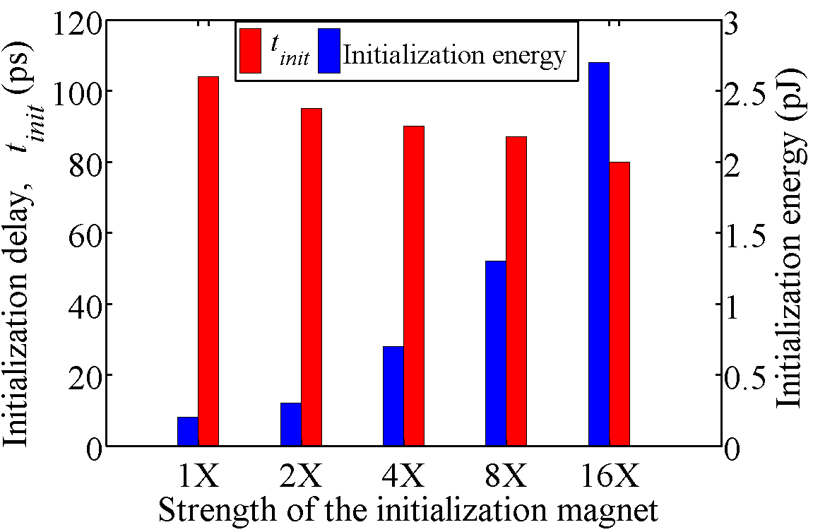
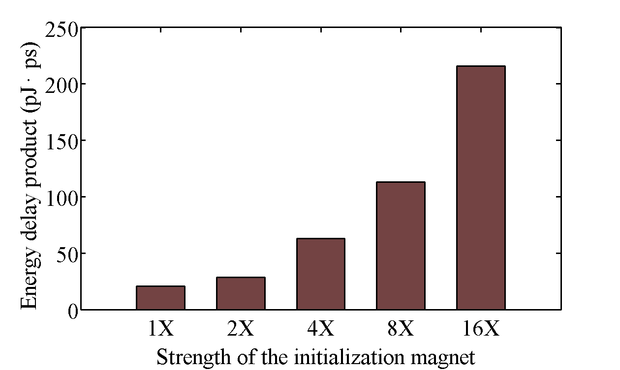
The energy, delay, and energy-delay product for initialization are plotted in Fig. 14. In this work, we choose the solution with the optimal energy-delay product, corresponding to a 1 magnet. This result can be explained by the fact that due to spin losses in the channel, increasing the input magnet size does not reduce the delay sufficiently to compensate for the corresponding increase in energy. Therefore, we use the 1 magnet for initialization, which corresponds to ps and initialization energy of pJ. In other words, based on this analysis, although it is possible to speed up initialization, we choose to go with the solution that is similar to the conventional ASL scheme. The circuit-level analysis in Section IV-B as well as the adder optimizations to be proposed in Section VI-C both support this choice, since the initialization phase can be overlapped with evaluation for all but the first stage of logic. If it is important to reduce the circuit delay, the value of only the first logic stage can be made faster, at the expense of a special narrow clock signal for this stage.
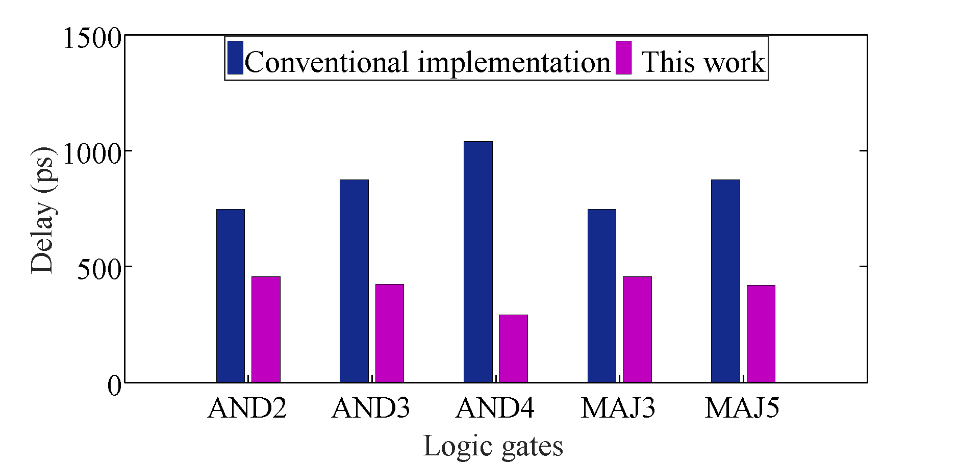
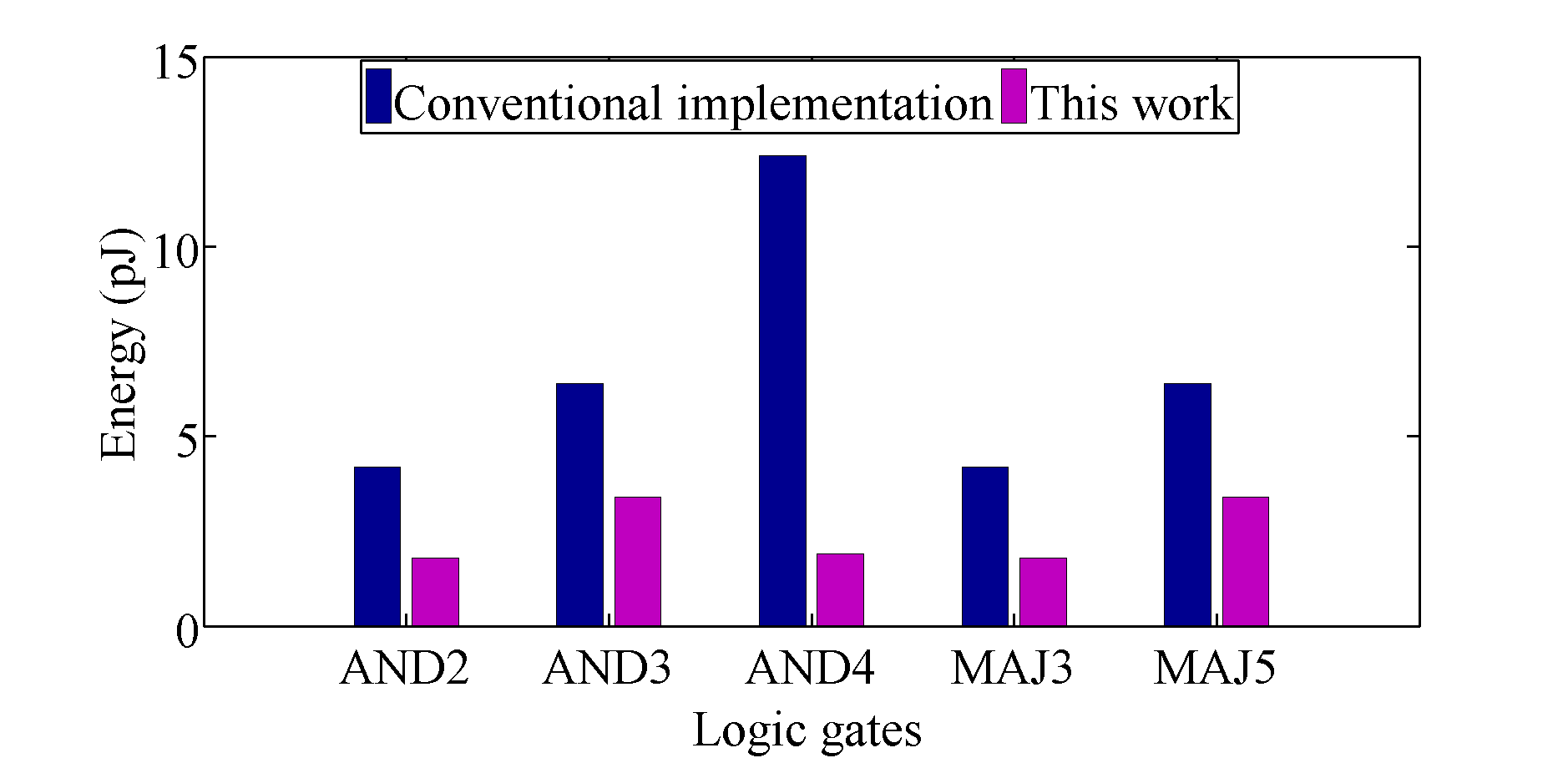
We compare the delay and energy associated with the conventional ASL implementation and STEM with respect to the AND2, AND3, AND4, MAJ3, and MAJ5 logic gates, and display the results in Fig. 15. For each logic gate, the delay for the STEM implementation refers to the sum of the initialization delay, and the evaluation delay, . We note that this may understate the advantage of STEM: as observed in Section IV-B, the phase can be overlapped with the evaluation of the next gate since the delay penalty for initialization is paid only once in the first logic stage. Compared to STEM, the AND2, AND3, and AND4 implementations using conventional ASL are, respectively, , , and slower and , , and less energy-efficient. The large delay and energy improvements for AND4 are primarily due to a reduction from a total of seven input magnets with the conventional ASL implementation to five input magnets for STEM.
From a delay and energy perspective, the MAJ3 gate is substantially similar to the AND2 structure and sees the same level of improvement. A similar analysis on MAJ5 gates shows that the conventional ASL implementation is slower than STEM, while being less energy-efficient. As before, the advantage of STEM is larger for gates with more inputs.
VI-B Impact of thermal fluctuations on the switching delay
The switching delay of a ferromagnet in Equation (7) is obtained as a deterministic number by solving the Landau-Lifshitz-Gilbert-Slonczewski (LLGS) equation [16]. However, the switching process is indeterministic owing to the impact of random thermal fluctuations. Here, we study the variations in the switching delay with the example of an AND3 gate using the HSPICE model for stochastic LLGS [19] at room temperature. The AND3 circuit is modeled using the method described in Section V. The spin current, , at the output magnet obtained by solving Equation (6) is provided to the stochastic LLGS solver to obtain a distribution for the delay.
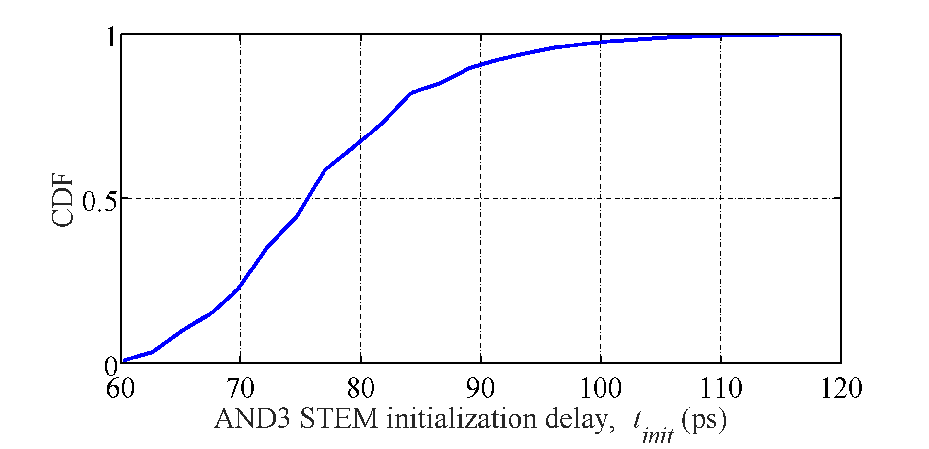
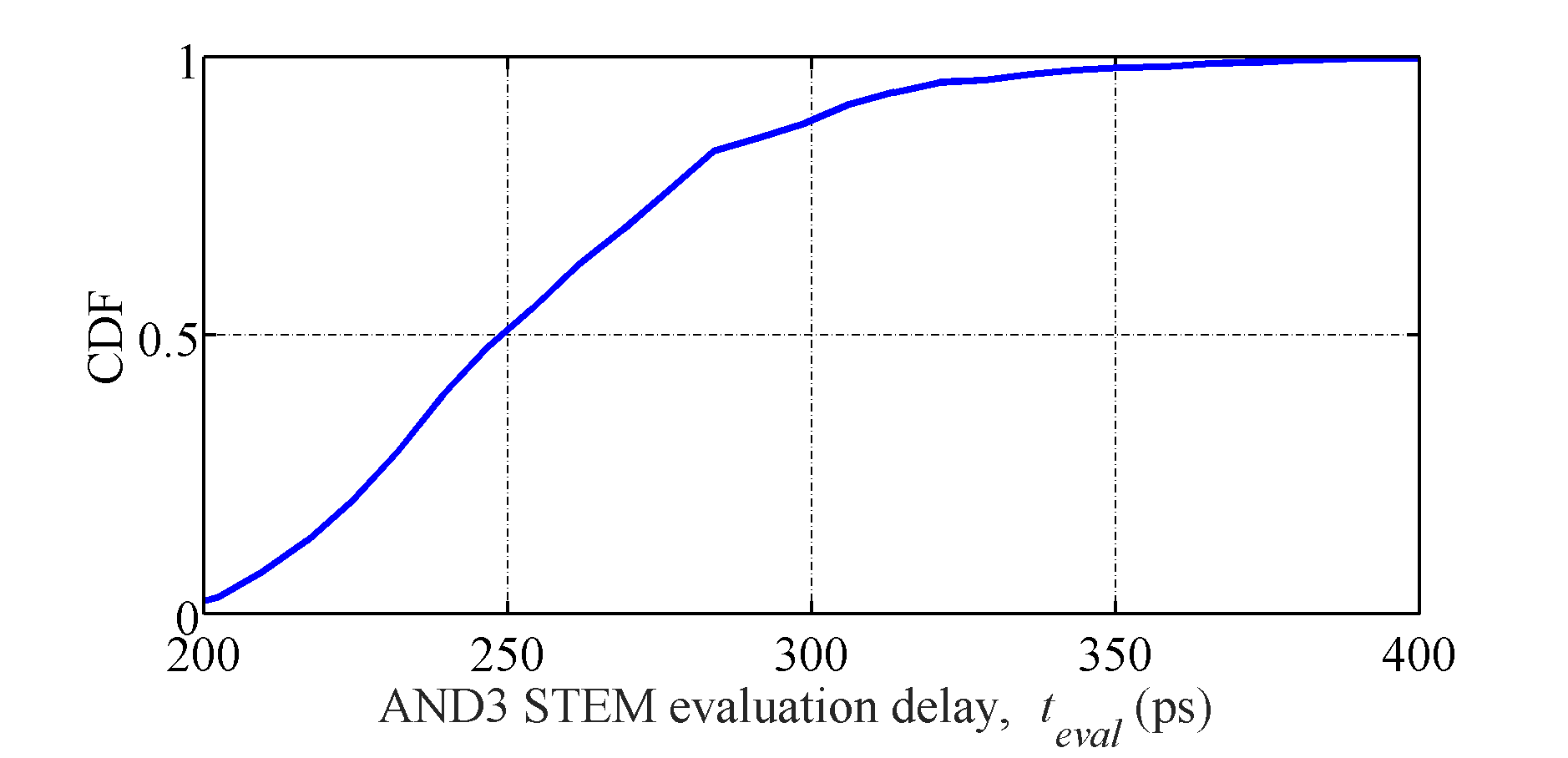
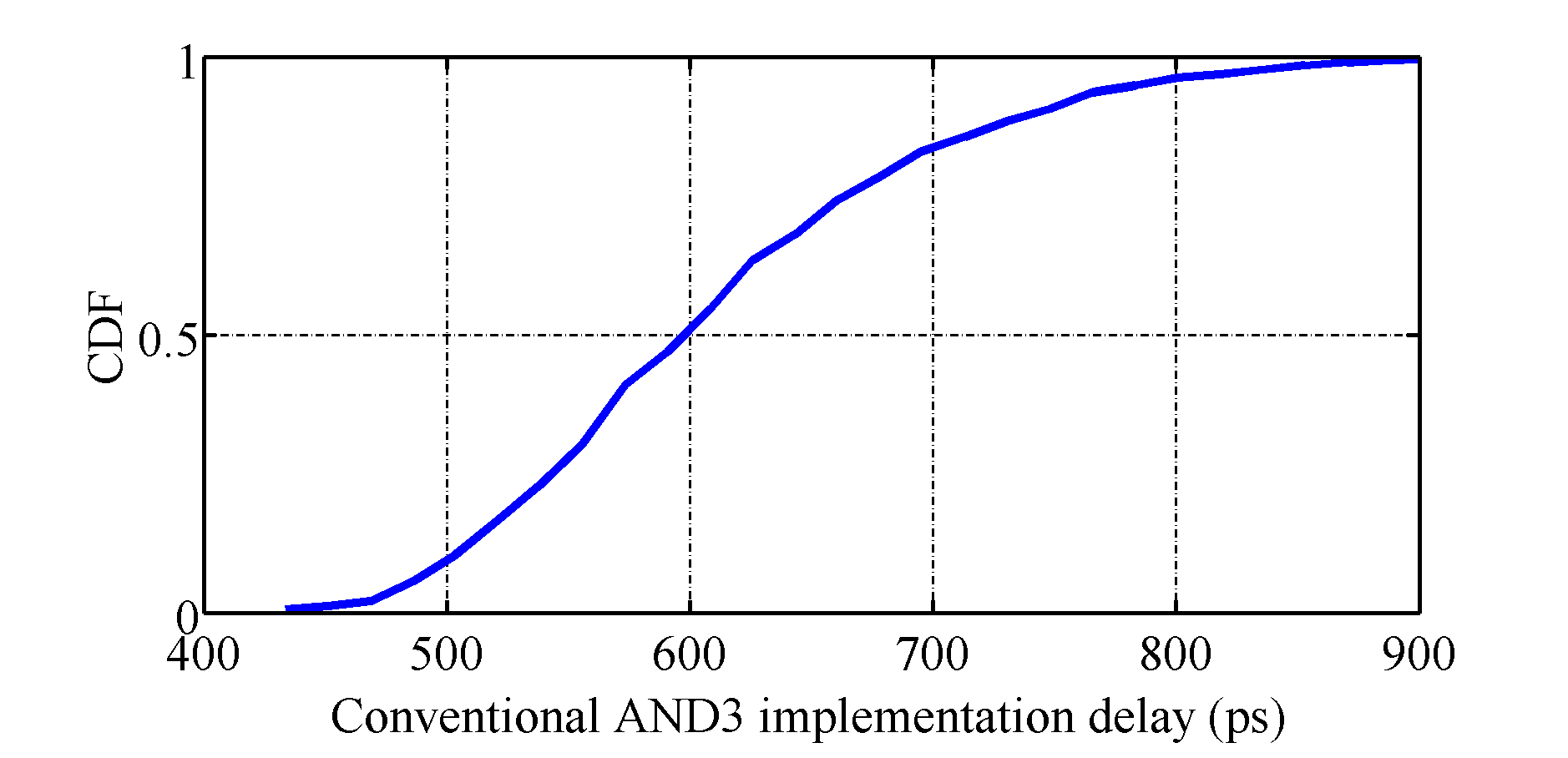
The cumulative distribution function (CDF) of the initialization and the evaluation delay of the AND3 gate implemented using STEM scheme is shown in Figs. 16(a) and 16(b), respectively, while the corresponding CDF for the conventional implementation is shown in Fig. 16(c). The deterministic delay of Equation (7) corresponds to the 99 percentile switching probability obtained from the stochastic LLGS solver. The 99 percentile point of the delay of the AND3 gate implemented using STEM scheme is the sum of the 99 percentile point of the initialization and the evaluation delays. This ensures that the initialization of the output magnet of the AND3 is complete before the evaluation phase begins. The AND3 STEM delay is thus obtained as . The 99 percentile point corresponds to a delay of for the AND3 gate implemented conventionally, which is approximately twice that of the STEM implementation. These numbers are consistent with the delays reported in Fig. 15(a).
We make two important observations from Fig. 16:
-
1.
The delay distribution of the AND3 gate implemented with the conventional scheme is broader compared to that of the AND3 gate implemented with the STEM scheme. This result is consistent with the findings in [20], which shows that the broadening of the delay distribution occurs when the magnitude of the spin current that switches the output magnet is lowered. A lower spin current requires a larger initial angle of the magnetization which in turn leads to a larger time for the magnetization to achieve the 99 percentile point. In the case of the conventional AND3 implementation, the magnitude of the spin current that switches the output magnet is less than that compared to the STEM scheme as explained in detail in Sections II-A and II-B, leading to a broader delay distribution.
-
2.
The stochastic nature of the magnet switching during the initialization and the evaluation phase for STEM dictates the pulse widths of the “init” and the “eval” signals. This is to ensure that the initialization (evaluation) of the output magnet is complete when the “init” (“eval”) signal is deasserted.
VI-C Evaluating the five-magnet adder
We show the impact of using STEM for implementing the five-magnet adder, as described in Section IV-C, and compare the delay and energy savings with respect to the conventional ASL implementation. We model the adder circuit in MATLAB using the method described in Section V. Using the notation defined in Section IV-C, the layout shown in Fig. 11(b), and the simulation parameters in Table III, we find that , , , and .
These results can be explained by referring to the four-step operation of the full adder implemented with STEM presented in Section IV-C.
-
•
The initialization of is performed using input in step one. The requirement to achieve symmetry between the input magnets, , , and , for the evaluation of in step four, prevents us from placing input magnet closer to , for a faster initialization in step one. This results in a 1X current strength initializing , while in step two, a 2X current from input magnets, and , from STEM MAJ3 implementation evaluates . Therefore, .
-
•
In step three, initializes , while in step four, is evaluated as MAJ3(,,). Thus, there is no requirement for symmetry between the input magnets and for the evaluation of . This allows the placement of such that we obtain a compact layout for the full adder with STEM scheme as shown in Fig. 11(b). In comparison, the full adder layout obtained using the conventional implementation occupies more area as seen from Fig. 11(a). The evaluation of in the conventional implementation as MAJ5(,,, ,) requires careful balancing of channel segment lengths to achieve symmetry between the input magnets and , thereby occupying more area.
-
•
Moreover, a 3X net current evaluates in step four compared to the 2X current strength that evaluates in step two. Therefore, we obtain .
-
•
The channel length between input magnet and is longer compared to the channel length between and . This results in .
We begin with the basic timing diagram of Fig. 12. The timing diagram with the relative pulse-widths of the initialization and evaluation signals for the full adder implemented using the STEM technique is shown in Fig. 17. Since it is preferable to generate a single evaluation pulse that can be applied to the gates, we set a safe value of and applied to both gates. We therefore delay the “eval” signal to by time units, and extend the pulse duration to equal time units. We also extend the “eval” signal to for an additional units. The resulting timing diagram shown in Fig. 17 is identical to Fig. 12 with and . The total delay of the full adder implemented with the STEM scheme is given by, .
| Adder implementation | Delay (ps) | Energy (pJ) | Area (nm2) |
|---|---|---|---|
| Conventional ASL | 2349 | 13.6 | 11250 |
| STEM | 1590 | 6.3 | 9450 |
For the simulation parameters in Table III and under the spin circuit model in Section V, the delay, energy, and area for the full adder in the conventional ASL implementation and STEM are shown in Table IV. The full adder delay using conventional ASL scheme, , is the sum of the delays of MAJ3 gate (to calculate ) and the MAJ5 gate (to calculate ). Here, both MAJ3 and MAJ5 gates are implemented using the conventional ASL scheme. Compared to the conventional implementation, we see that the full adder implemented with STEM is faster and more energy-efficient, and provides a 16% improvement in area.
VII Conclusion
In this work, we have proposed STEM, a novel two-phase method that leverages the delay dependence of the device while implementing the majority logic. In the first phase, the output is initialized to a preset value, while in the second stage the inputs evaluate to switch the output under a time constraint. We demonstrate this idea on standard cells built with ASL gates. We show that an -input AND gate which requires inputs with conventional ASL can now be implemented with just inputs. We show that STEM significantly outperforms conventional ASL in terms of delay as well as energy: STEM ASL gates are faster while being more energy-efficient as compared to conventional ASL gates, STEM ASL majority gates are faster and more energy-efficient than conventional, and a STEM ASL five-magnet full adder is faster, more energy-efficient, and more area-efficient than its conventional counterpart. Further circuit-level and system-level optimizations are possible. Like CMOS domino logic [21], the STEM logic family is very amenable to pipelining and we believe that many of the methods used to pipeline domino logic carry over to STEM.
References
- [1] D. E. Nikonov and I. A. Young, “Overview of beyond–CMOS devices and a uniform methodology for their benchmarking,” Proceedings of the IEEE, vol. 101, no. 12, pp. 2498–2533, Dec 2013.
- [2] C. S. Lent, P. D. Tougaw, W. Porod, and G. H. Bernstein, “Quantum cellular automata,” Nanotechnology, vol. 4, no. 1, pp. 49–57, 1993.
- [3] P. D. Tougaw and C. S. Lent, “Logical devices implemented using quantum cellular automata,” Journal of Applied Physics, vol. 75, no. 3, pp. 1818–1825, 1994.
- [4] A. Imre, G. Csaba, L. Ji, A. Orlov, G. H. Bernstein, and W. Porod, “Majority logic gate for magnetic quantum-dot cellular automata,” Science, vol. 311, no. 5758, pp. 205–208, Jan 2006.
- [5] B. Behin-Aein, D. Datta, S. Salahuddin, and S. Datta, “Proposal for an all-spin logic device with built-in memory,” Nature Nanotechnology, vol. 5, no. 4, pp. 266–270, Feb 2010.
- [6] S. Datta, S. Salahuddin, and B. Behin-Aein, “Non–volatile spin switch for Boolean and non–Boolean logic,” Applied Physics Letters, vol. 101, no. 25, pp. 252 411–1–252 411–5, Dec 2012.
- [7] S. C. Chang, S. Manipatruni, D. E. Nikonov, and I. A. Young, “Clocked domain wall logic using magnetoelectric effects,” IEEE Journal on Exploratory Solid–State Computational Devices and Circuits, vol. 2, pp. 1–9, Dec 2016.
- [8] M. G. Mankalale, Z. Liang, A. Klemm Smith, Mahendra D. C., M. Jamali, J.-P. Wang, and S. S. Sapatnekar, “A fast magnetoelectric device based on current-driven domain wall propagation,” in Proceedings of the IEEE Device Research Conference, 2016.
- [9] J. Kim, A. Paul, P. A. Crowell, S. J. Koester, S. S. Sapatnekar, J.-P. Wang, and C. H. Kim, “Spin-based computing: Device concepts, current status, and a case study on a high-performance microprocessor,” Proceedings of the IEEE, vol. 103, no. 1, pp. 106–130, Jan 2015.
- [10] C. S. Lent and B. Isaksen, “Clocked molecular quantum-dot cellular automata,” IEEE Transactions on Electron Devices, vol. 50, no. 9, pp. 1890–1896, Aug 2003.
- [11] C. S. Lent, M. Liu, and Y. Lu, “Bennett clocking of quantum-dot cellular automata and the limits to binary logic scaling,” Nanotechnology, vol. 17, no. 16, pp. 4240–4251, Aug 2006.
- [12] M. C. Chen, Y. Kim, K. Yogendra, and K. Roy, “Domino-style spin orbit torque-based spin logic,” IEEE Magnetics Letters, vol. 6, pp. 1–4, 2015.
- [13] H. M. Martin, “Threshold logic for integrated full adder and the like,” 1971, US Patent 3,609,329.
- [14] C. Augustine, G. Panagopoulos, B. Behin-Aein, S. Srinivasan, A. Sarkar, and K. Roy, “Low-power functionality enhanced computation architecture using spin-based devices,” in Proceedings of the IEEE/ACM International Symposium on Nanoscale Architectures, 2011, pp. 129–136.
- [15] S. Srinivasan, V. Diep, and B. Behin-Aien, “Modeling multi-magnet networks interacting via spin currents,” 2013, available at http://arxiv.org/abs/1304.0742.
- [16] B. Behin-Aein, A. Sarkar, S. Srinivasan, and S. Datta, “Switching energy-delay of all spin logic devices,” Applied Physics Letters, vol. 98, no. 12, pp. 123 510–1–123 510–3, Mar 2011.
- [17] M. G. Mankalale and S. S. Sapatnekar, “Optimized standard cells for all–spin logic,” ACM Journal on Emerging Technologies in Computing, vol. 13, no. 21, Nov 2016.
- [18] M. Sharad, K. Yogendra, K. Kwon, and K. Roy, “Design of ultra high density and low power computational blocks using nano-magnets,” in Proceedings of the IEEE International Symposium on Quality Electronic Design, 2013, pp. 223–230.
- [19] K. Y. Camsari, “Stochastic Landau-Lifshitz-Gilbert Module,” https://nanohub.org/groups/spintronics/llg_thermal_noise, accessed: 2017-01-08.
- [20] W. H. Butler, T. Mewes, C. K. A. Mewes, P. Visscher, W. H. Rippard, S. E. Russek, and R. Heindl, “Switching distributions for perpendicular spin-torque devices within the macrospin approximation,” IEEE Transactions on Magnetics, vol. 48, pp. 4684–4700, Dec 2012.
- [21] D. Harris and M. A. Horowitz, “Skew-tolerant domino circuits,” IEEE Journal of Solid-State Circuits, vol. 32, no. 11, pp. 1702–1711, Nov 1997.