Interface Engineering in La0.67Sr0.33MnO3–SrTiO3 Heterostructures
Abstract
Interface engineering is an extremely useful tool for systematically investigating materials and the various ways materials interact with each other. We describe different interface engineering strategies designed to reveal the origin of the electric and magnetic dead-layer at La0.67Sr0.33MnO3 interfaces. La0.67Sr0.33MnO3 is a key example of a strongly correlated peroskite oxide material in which a subtle balance of competing interactions gives rise to a ferromagnetic metallic groundstate. This balance, however, is easily disrupted at interfaces. We systematically vary the dopant profile, the disorder and the oxygen octahedra rotations at the interface to investigate which mechanism is responsible for the dead layer. We find that the magnetic dead layer can be completely eliminated by compositional interface engineering such that the polar discontinuity at the interface is removed. This, however, leaves the electrical dead-layer largely intact. We find that deformations in the oxygen octahedra network at the interface are the dominant cause for the electrical dead layer.
I Introduction
Oxide epitaxy has made tremendous advances in the past 15 years. Using techniques such as pulsed laser deposition (PLD) and molecular beam epitaxy (MBE), oxide epitaxy has evolved from merely depositing material with the right crystal structure onto a substrate to growing the material in a layer-by-layer fashion. The latter allows interventions during the growth and therefore enables the creation of artificial materials. The progress in epitaxy is due not only to improvements in the growth systems and growth monitoring, but also to a better understanding of the ways materials influence each other during heteroepitaxy. Research has shown that perovskite oxide epitaxial layers are influenced by the boundary conditions applied by the epitaxy process. Properties are modified due to the presence of such phenomena as strain, polar discontinuities, and octahedral connectivity mismatch. This sensitivity offers the unique opportunity to engineer the materials’ structure. In this way, advanced epitaxy has become a research tool for understanding materials, because it allows different structural parameters to be disentangled. Some examples of the possibilities of advanced epitaxy are: tricolor superlattices Lee et al. (2005), compositional interface engineering Boschker et al. (2012a); Peng et al. (2014); Huijben et al. (2015), modulation doping Chen et al. (2015), oxygen octahedra rotation engineering Bousquet et al. (2008); Boschker et al. (2012b); Rondinelli et al. (2012); Aso et al. (2014); Moon et al. (2014); Zhai et al. (2014), interface dipole engineering Yajima et al. (2011), transfer of electron-phonon coupling Driza et al. (2012), and defect mitigation Lee et al. (2013).
La0.67Sr0.33MnO3 is interesting because it is a ferromagnetic metal with 100 % spin polarization Park et al. (1998). It is therefore relevant to a variety of devices such as magnetic tunnel juctions Sun et al. (1999); Bowen et al. (2003), diodes Postma et al. (2004); Hikita et al. (2009), transistors Yajima et al. (2011), and ferroelectric tunnel junctions Garcia et al. (2010). All of these applications require control of the properties of La0.67Sr0.33MnO3 at the interface. The half-metallic state in La0.67Sr0.33MnO3 arises from a complex balance between competing interactions. The double exchange interaction favors conductivity whereas the superexchange interaction favors an insulating state. Furthermore, the material is susceptible to Jahn-Teller distortions that also favor electron localization. All these factors depend on the local crystal environment of the Mn ions. At interfaces the balance between the competing interactions is modified and an electrical and magnetic dead-layer is present Kavich et al. (2007); Huijben et al. (2008).
Here we present a study of different interface engineering schemes for La0.67Sr0.33MnO3 interfaces with a focus on the La0.67Sr0.33MnO3–SrTiO3 interface. The goal is to systematically investigate different mechanisms thought to be responsible for the dead-layer behavior. In the following sections we discuss the polar discontinuity problem, the effect of disorder, and the oxygen octahedra rotations.
II Experimental
SrTiO3 substrates were prepared using a standard BHF etching procedure Koster et al. (1998). The La0.67Sr0.33MnO3 thin films were grown with pulsed laser deposition (PLD) (TSST system). The substrate temperature during growth was 750-800 ∘C in an oxygen environment of 0.27 mbar. The laser beam was produced by a 248-nm-wavelength KrF excimer laser (LPXPro from Coherent, Inc.) with a typical pulse duration of 20-30 ns. With a 4 by 15 mm rectangular mask the most homogeneous part of the laser beam was selected. A sharp image of the mask was created on the stoichiometric target (Praxair electronics) with a lens, resulting in a spotsize of 2.3 mm2 (0.9 by 2.5 mm). The beam energy was controlled with a variable attenuator or with the laser voltage, yielding a fluence at the target of 2 J/cm2. The repetition rate was 1 Hz and the substrate was placed at 5 cm distance directly opposite to the target. Before deposition, the target was pre-ablated for 2 minutes at 5 Hz to remove any possible surface contamination. After deposition, the PLD chamber was flooded with pure oxygen (typically 100 mbar) and the samples were cooled down by switching of the heater power. Typically, the cooldown required 2 hours. For the PLD growth of SrTiO3 and SrMnO3, identical settings were used as for the La0.67Sr0.33MnO3 growth. For the LaTiO3 growth, and the growth of the SrTiO3 layer on top of the LaTiO3, the deposition pressure was lowered to 3 mbar, in order to prevent the formation of La2Ti2O7 Ohtomo et al. (2002). Some of the thicker La0.67Sr0.33MnO3 films were grown with a repetition rate of 5 Hz and an oxygen pressure of 0.16 mbar.
The magnetization of the samples was measured with a vibrating sample magnetometer (VSM) (Physical Properties Measurement System (PPMS) by Quantum Design). In order to determine the saturation magnetization and Curie temperature unambiguously, magnetic hysteresis loops were obtained at all temperatures as discussed in detail in the supplementary information of Boschker et al. (2012a). The resistivity of the samples was measured in the van der Pauw configuration van der Pauw (1958) (PPMS by Quantum Design). In order to obtain ohmic contacts between the aluminium bonding wires and the La0.67Sr0.33MnO3 layer, gold contacts were deposited on the corners of the sample with the use of a shadow mask. The electric field gating experiments were performed with a backgate geometry, using the 0.5 mm substrate as a gate dielectric. In order to ensure a uniform electric field, the back of the substrate was glued to a copper plate using silver epoxy.
III Thin film growth and characterization
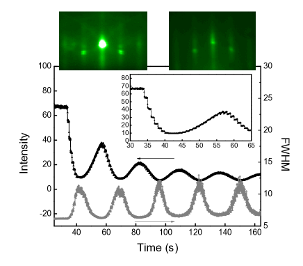
The growth of the films was studied in situ with RHEED during the growth. The substrate RHEED pattern is shown in Fig. 1 on the top left. The main specular spot is very intense compared to the two side spots. This is the typical signature of TiO2 terminated SrTiO3 Koster et al. (2000). Kikuchi lines are visible as well, indicating the smoothness of the substrate. The side spots are doubled, which is due to the additional periodicity at the surface from the regularly spaced terrace steps. Figure 1, top right, shows the RHEED image of the La0.67Sr0.33MnO3 film after the deposition of 5 unit cell layers. Clear two dimensional spots are visible, but also 2D streaks are present. The latter are attributed to the scattering of the RHEED beam off the unit cell high steps at the surface. Similar RHEED images were observed after the completion of films with thicknesses up to 40 nm.
The main graph in Fig. 1 shows the intensity of the specular reflection as measured during the initial growth of La0.67Sr0.33MnO3. The intensity shows oscillations which correspond to the growth of the individual unit cell layers. Within the oscillations, recovery of the intensity after the sudden decrease during the laser burst is observed, as shown more clearly in the inset of the graph. The oscillation amplitude decreases with the amount of material deposited during the first part of the growth. This decrease of the intensity is due to the difference in reflectivity of the SrTiO3 surface and the La0.67Sr0.33MnO3 surface, due to the increased scattering from the heavy La ions in the lattice. Finally, the full width at the half maximum (FWHM) of the intensity of the specular spot, measured along the (10) direction, is presented as well. During the growth, the RHEED spots are periodically more streaky, because more stepedge scattering is present at half unit cell layer coverage compared to full unit cell layer coverage. Therefore, the FWHM oscillates as well. The FWHM depends only on the shape of the intensity distribution and not on the total intensity and it is therefore a better indicator of the surface morphology than the main intensity of the reflection. As can be seen in the figure, the FWHM during the growth is almost equal to the FWHM of the substrate reflection indicating a smooth surface morphology. From these measurements it is concluded that the initial stage of the La0.67Sr0.33MnO3 growth proceeds in the ideal 2D layer-by-layer growth mode.
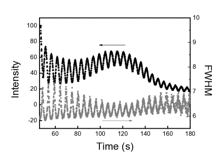
During the growth of the film, an increase of the RHEED oscillation maximum intensity was observed, as presented in Fig. 2. The oscillation intensity maximum typically peaked around 20 to 25 unit cell layers. The maximum in intensity was not observed during growth on an -site terminated substrate surface, so it might indicate a termination conversion. After this peak the oscillation intensity maximum decreased rapidly and the oscillation amplitude became comparable to the intensity variations in the laser pulse recovery cycles. It is concluded that the La0.67Sr0.33MnO3 growth mode during the latter part of the growth is close to the steady state growth mode which is characterized by a relatively constant step density, which is large compared to the step density of the initial substrate surface.
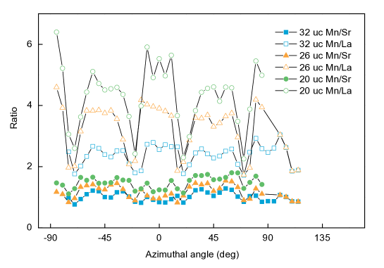
In order to check the hypothesis about a termination conversion during growth, three samples with respectively a 20, 26 and 30 unit-cell-thick La0.67Sr0.33MnO3 layer were measured with angle-dependent time-of-flight mass spectroscopy. The relative intensity of the Mn ions with respect to Sr and La is shown in Fig. 3. The strong angular dependence in the Mn/La ratio of the 20 unit-cell-thick sample is consistent with a dominant MnO2 crystal termination. With increasing film thickness the angular dependence is reduced indicating a reduction of the MnO2 termination. The data is more consistent with a mixed termination for the thicker films than with a complete surface termination conversion. The Mn/Sr ratio has a similar angular dependence, although the magnitude of the signal is reduced. The lower Mn/Sr ratio compared to Mn/La is also seen in experiments using controlled O and O2 terminated La0.67Sr0.33MnO3 films Yu et al. (2012). In conclusion, the surface termination changes around 26 unit cells towards mixed termination, in agreement with the deductions from the growth analysis.
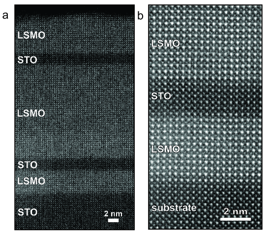
A multilayer La0.67Sr0.33MnO3–SrTiO3 sample was characterized with scanning transmission electron microscopy (STEM), to study the interface atomic structure. The STEM data presented was measured with a FEI Titan microscope. The sample is comprised of several layers, from substrate to surface: 4 nm La0.67Sr0.33MnO3, 2 nm SrTiO3, 16 nm La0.67Sr0.33MnO3, 2 nm SrTiO3 and 8 nm La0.67Sr0.33MnO3.
Figure 4a presents a low magnification HAADF image of the different layers in the sample. In HAADF microscopy, the observed intensity of a column of atoms scales with the atomic weight of the elements within the columns. Therefore, the La0.67Sr0.33MnO3 is brighter in the image than the SrTiO3. Figure 4b presents a higher magnification image obtained from the layers close to the substrate. Both the - and -site columns are observed. The multilayer structure is grown coherently and following a quantitative analysis by statistical parameter estimation Van Aert et al. (2009), it can be concluded that the interfaces are well defined with a chemical roughness of maximum 1 unit cell.
The La0.67Sr0.33MnO3–SrTiO3 heterostructures have not only excellent structural properties, but they also have excellent functional properties. Thicker films of 10 nm show a Curie temperature of 350 K, a low-temperature saturation magnetization of 4 /Mn, and a residual resistivity of 60 cm. The heterostructures compare favourably to the samples presented in the literature Boschker et al. (2011). The combination of high-quality films with excellent functional properties and the two-dimensional layer-by-layer growth allows for the interface engineering described in the remainder of this chapter. However, because atomic control of the crystal termination during growth is only possible up to a finite film thickness, reliable interface engineering can only be performed for thin La0.67Sr0.33MnO3 heterostructures.
IV Polar discontinuities at the interface
La0.67Sr0.33MnO3–SrTiO3 interfaces are polar and therefore ionic or electronic reconstructions are to be expected. Two different atomic stacking sequences are possible for the La0.67Sr0.33MnO3–SrTiO3 interfaces, due to the possible O or O2 termination of each material. One will be referred to as the La0.67Sr0.33O terminated interface and the other as the MnO2 terminated interface. The La0.67Sr0.33O terminated interface is shown in Fig. 5a. At this interface the atomic stacking sequence is SrO-TiO2-La0.67Sr0.33O-MnO2. The MnO2 terminated interface is shown in Fig. 5b. Here the atomic stacking sequence is TiO2-SrO-MnO2-La0.67Sr0.33O. Both interface configurations are polar, and without reconstruction would result in a diverging electrostatic potential, as indicated in the figures. As La0.67Sr0.33MnO3 is conducting, the mobile charges can screen the diverging potential. This screening, however, is only partial due to the fact that the charges are confined to the Mn sublattice. In Fig. 5a and 5b the electrostatic potential after the screening (effectively an electronic reconstruction of the polar discontinuity) is shown as well. Here it is assumed that the screening occurs completely in the first MnO2 layer, which is consistent with the Thomas Fermi length of La0.67Sr0.33MnO3 of 0.31 nm Hikita et al. (2009). The diverging potential is eliminated, but a band offset, especially in the case of the La0.67Sr0.33O terminated interface, is present and will result in intermixing of the cations Nakagawa et al. (2006). Note that the Ti4+ valence state is stable at all these interfaces, as the Ti t2g levels are 1 eV higher in energy compared with the Mn eg levels Kumigashira et al. (2006).
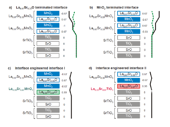
In order to remove the polar discontinuity, an sub-unit-cell atomic layer with a net charge of 1/3 -/uc has to be inserted at the interface. This is shown in Fig. 5c and 5d, in which two methods are shown for interface engineering by inserting a single atomic layer of La0.33Sr0.67O between the two materials through the deposition of either a La0.33Sr0.67MnO3 layer (I) or a La0.33Sr0.67TiO3 layer (II). This gives an atomic stacking sequence at the interface of SrO-TiO2-La0.33Sr0.67O-MnO2-La0.67-Sr0.33O. In this case, the diverging potential is absent and no driving force for reconstruction exists. A band offset is present at this interface as well, so some intermixing can still be expected.
Several heterostructures with and without interface engineering (denoted IE and non-IE, respectively) were grown. The structures consist of a TiO2 terminated STO substrate, a variable thickness La0.67Sr0.33MnO3 layer and a SrTiO3 cap layer with a thickness of five unit cells. In order to realize the interface engineered heterostructure, first a single unit cell layer of La0.33Sr0.67MnO3 was grown. This was followed with the growth of -1 layers of La0.67Sr0.33MnO3, then a single unit cell layer of La0.33Sr0.67TiO3 and finally, four unit cell layers of SrTiO3. This recipe resulted in heterostructures with layers of Mn ions, which can therefore be compared with the unit cell layer La0.67Sr0.33MnO3–SrTiO3 structure without the interface engineering. Next to the single layer samples, also two superlattice samples (IE and non-IE) with five repetitions of (La0.67Sr0.33MnO3)8(SrTiO3)5 were grown.
The samples were analyzed extensively by STEM and electron energy loss spectroscopy (EELS) Boschker et al. (2012a); Huijben et al. (2015). It was found that in the non-IE samples differences between the top and bottom interface exist, due to the difference in stacking sequence at the interface. At the bottom interface (La0.67Sr0.33O terminated interface) a relatively large diffusion of La ions into the SrTiO3 was found which is probably the result of a reconstruction of the polar discontinuity. In contrast, the IE samples show similar top and bottom interfaces, in agreement with the design of the heterostructures.
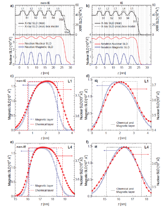
The depth profiles of the magnetization in the superlattice samples was measured with polarized neutron reflectometry (PNR) Huijben et al. (2015). The main result of the analysis is shown in Fig. 6. These profiles show that the topmost SrTiO3 and La0.67Sr0.33MnO3 layers exhibited different structural properties, most likely due to relaxation at the surface. However, all other four buried La0.67Sr0.33MnO3–SrTiO3 bilayers showed to be structurally equal as demonstrated by showing the first (L1) and fourth (L4) La0.67Sr0.33MnO3 layer in respectively Figs. 6c,e and 6d,f. The chemical roughnesses in the IE heterostructure are typically 1.5 times larger than that in the non-IE heterostructure. This can to some degree be attributed to the more gradual La distribution in the design of the IE heterostructure. The magnetic roughnesses, in contrast, are similar in both heterostructures.
Most importantly, for the non-interface-engineered (non-IE) heterostructure a clear 5.5 Å 1.0 Å difference between the magnetic and chemical thickness of the La0.67Sr0.33MnO3 layer was observed (Figs. 6c and 6e). The optimal model indicates that only the top part of each La0.67Sr0.33MnO3 layer was strongly magnetically reduced. Because the La profile in the non-IE structures is shifted with respect to the Mn profile (STEM-EELS measurements), we also tested an alternative model with equally sized dead-layers at both interfaces. The model also yields a total 5 Å magnetically dead region (2.5 Å each at top and bottom interfaces), similar to the optimal model, albeit with a slightly increased fitting error. Note that the difference between magnetic and chemical profiles at the bottom interface is largely due to La diffusion, as the first Mn layer is still magnetic. On the other hand, at the top interface, a reduction of the magnetization is found in a layer where Mn exists, therefore a true magnetic dead-layer La0.67Sr0.33MnO3 only resides at the top interface. This is in good agreement with a previous observation that a surpluss of La does not deteriorate the magnetism Kavich et al. (2007). Overall, in the non-interface engineered heterostructure, the magnetic thickness is 5 Å less than the chemical thickness, and there is at least a magnetically reduced region at the top, and possibly at the bottom, the combination of which is 5.5 Å 1.0 Å thick.
In contrast, the interface-engineered (IE) heterostructure demonstrated an equal magnetic and chemical thickness of the La0.67Sr0.33MnO3 layer (Figs. 6d and 6f). The integrated magnetization at 120 K over the eight unit-cell-thick La0.67Sr0.33MnO3 layer, extracted from the PNR data, is 3.3 /Mn for the heterostructure with interface engineering, while a heterostructure without interface engineering exhibited a magnetization of only 2.8 /Mn. The absolute magnetization values extracted from PNR are confirmed by VSM measurements and the observed magnetization enhancement of 18 % is in very good agreement with the observed increase in magnetization of a single La0.67Sr0.33MnO3–SrTiO3 bilayer when interface engineering was applied.
Figure 7 presents temperature-dependent magnetization and resistivity measurements of the bilayer samples. The magnetic field was applied in-plane along the [100] SrTiO3 crystal direction during the magnetization measurements. Figure 7a shows the temperature dependence of the saturation magnetization for the = 5, 6, 8 and 13 uc samples. A clear difference between the IE and non-IE samples is observed. The IE samples have significantly higher saturation magnetization and Curie temperature (). Figure 7b presents the temperature dependence of the resistivity of the samples. For all thicknesses, the interface engineering results in a lower resistivity. The =5 samples and the non-IE =6 sample are insulating at low temperature. The =6 IE sample has an upturn in the resistivity at low temperature but conductivity was observed down to the lowest temperature (10 K) in the measurement. An enhancement of the magnetization and electrical conductivity can still be observed for thicker La0.67Sr0.33MnO3 layers in the 13 unit-cell-thick samples, however, the effect is smaller as the enhanced interface properties provide a smaller contribution to the properties of the complete La0.67Sr0.33MnO3 layer when thicker layers are studied. The obtained properties of the non interface engineered 13 uc sample are in good agreement with previously obtained results in ultrathin La0.67Sr0.33MnO3 films Huijben et al. (2008).
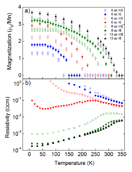
These results provide strong evidence of the elimination of a magnetic dead-layer at the La0.67Sr0.33MnO3–SrTiO3 interface when applying interface engineering by incorporating of a single La0.33Sr0.67O layer, which leads to embedding of the interfacial MnO2 atomic layer in between two (La,Sr)O layers. Furthermore, both the interface asymmetry of the magnetically reduced layer in the non-IE heterostructure and the absence of the dead-layer in the IE heterostructure confirm the reconstructions induced by the polar discontinuity at the interface as the origin of the former magnetic dead-layer at La0.67Sr0.33MnO3–SrTiO3 interfaces. However, even in the IE samples, the electrical dead-layer is still present and the question remains whether we can engineer even better interfaces.
V Order and disorder
La0.67Sr0.33MnO3 is a solid solution of LaMnO3 and SrMnO3. This implies La0.67Sr0.33MnO3 is an intrinsically disordered material, where the -site ion on a certain lattice site can be occupied with either a La or a Sr ion. It is an interesting question whether the disorder affects the properties, e.g. electrical transport. Several studies have presented results on the properties of (LaMnO3)2n/(SrMnO3)n superlattices, which have an identical La/Sr ratio with respect to La0.67Sr0.33MnO3 Yamada et al. (2006); Adamo et al. (2008); Bhattacharya et al. (2008). A decrease of the residual resistivity, with respect to the solid solution, was observed for the superlattice Bhattacharya et al. (2008).
Here, the effect of the disorder on the properties at the interface between La0.67Sr0.33MnO3 and SrTiO3 is studied. It is proposed that the SrTiO3–SrMnO3 interface has no intrinsic disorder, as the -site ions of both materials are equal. To obtain La0.67Sr0.33MnO3’s functional properties at the interface, charge has to be supplied to the SrMnO3 layer. This is accomplished by chemically doping the SrTiO3 away from the interface. This results in modulation doping Dingle et al. (1978), in which charge is transferred from the doped SrTiO3 layer to the SrMnO3 layer. The amount of charge which can be transferred is limited by the potential drop due to the electric dipole between the transferred electrons and the positively charged dopants. Eventually, the potential drop increases the energy of the SrMnO3 conduction band to the energy of the SrTiO3 conduction band and then the charge transfer stops. The maximum charge transfer is then given by:
| (1) |
in which is the maximum charge transfer, is the energy difference between the SrTiO3 and SrMnO3 conduction bands, is the permittivity of free space, is the dielectric constant and is the distance over which the charge transfer occurs. Therefore, the use of SrTiO3 has a great advantage; its huge dielectric constant screens the potential drop. It is possible to dope two -/uc over a distance of two nm, which is an order of magnitude larger as the charge transfer by modulation doping in semiconductor structures. And at low temperatures, significant charge transfer can be present without significant band bending, as the dielectric constant of SrTiO3 increases massively with decreasing temperature.
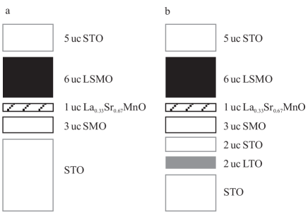
We tested the modulation doping scheme by growing two samples with ten unit-cell-thick manganite layers. A schematic image of the two samples is shown in Fig. 8. Sample A is a reference sample, where a SrMnO3 layer is inserted between the La0.67Sr0.33MnO3 and the SrTiO3 to obtain the SrTiO3–SrMnO3 interface. The thickness of the SrMnO3 layer is three unit cells, which corresponds to the amount of electrically dead layers at the La0.67Sr0.33MnO3–SrTiO3 interface. Next, a one unit-cell-thick layer of La0.33Sr0.67MnO3 is present between the SrMnO3 and the La0.67Sr0.33MnO3, as this results in higher quality growth of the La0.67Sr0.33MnO3. The La0.67Sr0.33MnO3 layer thickness is six uc, so the sample can be compared with an La0.67Sr0.33MnO3 sample with a thickness of ten unit cells. For this sample no dopants are present in the SrTiO3, so the La0.67Sr0.33MnO3 layer is expected to be overdoped. Sample B is similar to sample A, but here a two unit-cell-thick layer of LaTiO3 is inserted in the SrTiO3 two unit cells away from the interface. The LaTiO3 layer dopes two -/uc to the structure, which is precisely the amount required in the SrMnO3 layer to obtain La0.67Sr0.33MnO3’s Mn3.33+ valence state. Note that only the bottom interface has been engineered to remove the disorder, while the top interface is a disordered La0.67Sr0.33MnO3–SrTiO3 interface.
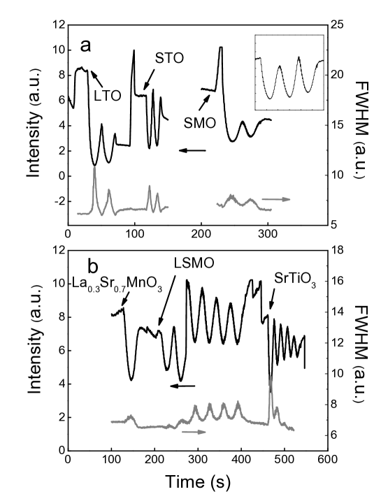
The intensity of the specular spot, as monitored with RHEED during the growth of sample B, is shown in Fig. 9. Clear oscillations are observed during the growth of LaTiO3 and SrTiO3. The initial growth of SrMnO3 on the LaTiO3–SrTiO3 stack started with an increase of the RHEED intensity to a maximum, followed by a prolonged oscillation. This second maximum occurred at the expected time for the deposition of 1.5 unit cell layers. The period of the second oscillation corresponds to the time required to deposit a single unit cell layer. As the SrMnO3 deposition was stopped at the third RHEED intensity maximum, only 2.5 unit cells of SrMnO3 instead of three were grown. This initial growth of SrMnO3 was not observed for the SrMnO3 growth directly on the SrTiO3 substrate. The inset of Fig. 9a shows the RHEED specular spot intensity observed during the SrMnO3 growth of sample A. Here three clear oscillations with equal periods are observed. After the growth of the SrMnO3, the growth of the La0.33Sr0.67MnO3, La0.67Sr0.33MnO3 and SrTiO3 layers showed RHEED oscillations. Therefore, it is concluded that the entire heterostructure was grown in 2D layer-by-layer fashion.
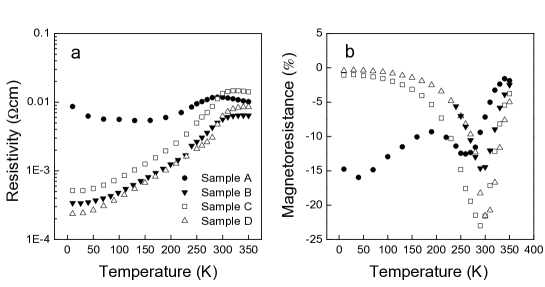
Electrical transport measurements of the samples are presented in Fig. 10. For comparison, also two other samples are shown. Sample C is a ten unit cell layer La0.67Sr0.33MnO3 sample capped with five unit cell layers of SrTiO3. Sample D is similar as sample C, but with engineered interfaces to remove the polar discontinuities, as discussed in section IV. The resisitivity of sample B is similar to the values observed for samples C and D, indicating that sample B has the properties of a ten unit cell layer La0.67Sr0.33MnO3 sample. Sample A, in contrast, has a higher resistivity, lower and negative magnetoresistance present at all temperatures. The transport behaviour of sample A is actually similar to that of seven unit-cell-thick La0.67Sr0.33MnO3 samples, consistent with the presence of seven unit cells of La0.67Sr0.33MnO3 in the sample structure. This result indicates that charge is transferred from the LaTiO3 layer to the SrMnO3 layer and that the charge transfer significantly changes the conductivity.

In order to verify that the optimum amount of charge is present in the SrMnO3 layer, electrical field effect measurements were performed. The charge carrier density of the sample can be controlled with the gate voltage applied to the back of the sample. Figure 11 presents the gate voltage dependence of the resistivity, measured at 10 K. Sample A shows some hysteretic behaviour, probably due to charge impurities in the SrTiO3 substrate, but the general dependence is monotonic with gate voltage. A decrease of the resistivity is observed for positive gate voltage (electron accummulation in the SrMnO3). This corresponds well with the expected overdoping of sample A. For sample B, a minimum in the resistivity is observed at a gate voltage of 50 V. This indicates that the optimum charge carrier density for the conductivity of the La0.67Sr0.33MnO3 is very close to the doping achieved with the modulation doping. With a SrTiO3 dielectric constant of 20000, at most 0.015 -/uc charge carriers are accummulated by the electric field. From a practical point of view, the control over the amount of dopants is 5% (approximately 1 laser pulse during deposition) of a unit cell layer of LaTiO3, which corresponds to 0.05 -/uc. Therefore, it is concluded that sample B is as good as can presently be realized and little room for improvement exists in optimizing the inserted amount of dopants. The experiments indicate that modulation doping with a significant charge transfer was achieved. However, La0.67Sr0.33MnO3’s conductivity at the interface was not much improved, indicating that disorder is not the key parameter governing the properties at the interface.
VI Octahedra rotations at the interface
In the preceeding sections we presented improvements of the La0.67Sr0.33MnO3 interface properties by removing the polar discontinuities and the intrinsic disorder at the interfaces. However, the electrical dead-layer still remains. The likely origin of the dead-layer lies in the structural reconstructions at the interface Pruneda et al. (2007); He et al. (2010). In this section we study the structure of the oxygen octahedra at the interface in detail.
The changes in the unit-cell symmetry resulting from different octahedral rotations have been systematized by Glazer Glazer (1972) and later expanded by Woodward Woodward (1997a, b). Octahedral rotations in the perovskite-type unit cell can be described as a combination of rotations about three symmetry axes of the pseudocubic unit cell. The relative magnitudes of the tilts are denoted by letters a, b, and c, .., aab means equal rotations around the and axes and a different tilt around the axis. Two adjacent octahedra around one of the 100 axes can rotate either in-phase or out-of-phase, which is indicated by the + or – sign, respectively. No rotation is indicated by the 0 sign.
SrTiO3 is a cubic crystal (above 105 K) with Glazer tilt system a0a0a0. La0.67Sr0.33MnO3 is rhombohedral with tilt system a-a-a-. La0.67Sr0.33MnO3 films grown on SrTiO3, however, have tilt system a+a-a0 in order to accommodate the tensile strain applied to the films Vailionis et al. (2011). Clearly a tilt system mismatch exists at the interface and because the oxygen octahedra network has to be continuous across the interface, structural distortions of the octahedra have to be present. These distortions have been predicted to occur on the La0.67Sr0.33MnO3 side of the interface He et al. (2010).
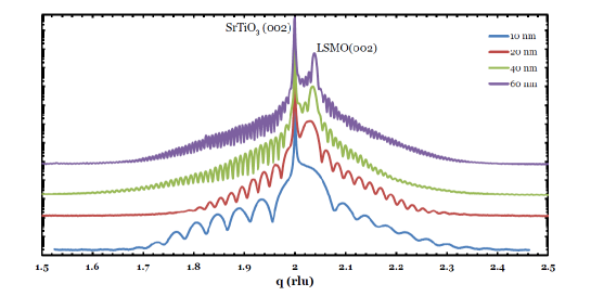
Four La0.67Sr0.33MnO3 samples with different thicknesses (10, 20, 40 and 60 nm) were studied with synchrotron x-ray diffraction (XRD). Figure 12 shows out-of-plane momentum scans around the (002) Bragg reflection. Next to the Bragg peaks, fringes are present due to the finite thickness of the samples. Due to the low surface and interface roughnesses in the samples a large number of fringes is seen and quantitative analysis is possible. The data contains two features that are inconsistent with the La0.67Sr0.33MnO3 having a uniform thickness throughout the sample: the fringe intensity at small momentum transfer (with respect to the Bragg peak) is larger than that at high momentum transfer and the fringe intensities exhibit a modulation with a larger period. Dynamical XRD calculations can only reproduce these features when several layers with different out-of-plane lattice parameters are included in the model of the sample structure Vailionis et al. (2014). Three distinct layers are present in the samples: an interface layer, an intermediate layer and the main layer, see Fig. 13.
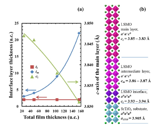
Here we focus on the interface layer. Surprisingly we find that the interface layer is two unit cells thick with an out-of-plane lattice parameter of 3.93-3.94 Å, independent of the total film thickness. This implies that the first atomic layers of the films are under compressive strain as opposed to the tensile strain in the rest of the films. The result can easily be understood by considering the interface mismatch in the oxygen octahedra rotation patterns between La0.67Sr0.33MnO3 and SrTiO3. The Mn-O bond length in La0.67Sr0.33MnO3 is 1.957 Å, so with the a0a0a0 tilt pattern of SrTiO3, the La0.67Sr0.33MnO3 would be cubic with a lattice constant of of 3.914 Å. This is larger than the lattice constant of SrTiO3 and the La0.67Sr0.33MnO3 interfacial layers are under compressive strain. The strain distorts the Mn-O bond length and, with a Poisson ratio of 0.4, the out-of-plane lattice parameter would be 3.93 Å, consistent with the experiment. In conclusion, the first two unit cells of La0.67Sr0.33MnO3 at the La0.67Sr0.33MnO3–SrTiO3 interface are severely distorted due to structural coupling to the SrTiO3. This interfacial layer has an a0a0a0 tilt pattern and the oxygen octahedra are elongated along the out-of-plane direction. We note that structural distortions are also found in photoemission experiments at this interface Gray et al. (2010, 2013). The elongation of the octahedra at the interface breaks the orbital symmetry and thereby the double exchange interactions are weakened at the interfaces.
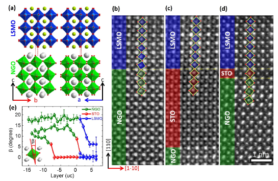
The situation is different in La0.67Sr0.33MnO3–NdGaO3 heterostructures. NdGaO3 is orthorhombic with the a-a-c+ tilt pattern, whereas La0.67Sr0.33MnO3 grown on NdGaO3 (110) has the a+b-c- tilt pattern Vailionis et al. (2011). These structural characteristics give rise to an in-phase vs. out-of-phase rotation type mismatch occurring along the [001]-axis that is absent along the [10]-axis where both materials’ rotations are out-of-phase. The magnitude of the bond angle also has a certain degree of mismatch: 154∘ in NdGaO3 vs. 166.3∘ in La0.67Sr0.33MnO3. As a result, both the anisotropic rotation type mismatch and the large difference (12∘) in bond angle will cause a strong discontinuity of the octahedra. In order to retain the connectivity of the corner shared oxygen octahedra across interface, the large octahedral tilt present in the NdGaO3 substrate will propagate into La0.67Sr0.33MnO3 near interface region, similar to what occurs in La0.67Sr0.33MnO3–SrTiO3 interfaces as mentioned above. Figure 14 presents STEM images of three La0.67Sr0.33MnO3–NdGaO3 heterostructures together with schematics of the bulk structures of the materials. A direct visualization of the octahedra rotations is possible with Cs-corrected STEM via which the oxygen atoms can be imaged through the angular bright field technique. Figure 14b clearly shows that NdGaO3 induces large rotations of octahedra in the La0.67Sr0.33MnO3 layers close to the interface. The octahedral tilt angle can be quantified by statistical parameter estimation theory Liao et al. (2016), and is presented in Fig. 14e. The tilt angle continuously changes from the NdGaO3 substrate value to that of bulk La0.67Sr0.33MnO3 (far from interface). Interestingly, the first two unit cell layers of the La0.67Sr0.33MnO3 have almost the same tilt angle as the NdGaO3. The impact of the octahedral coupling decays rapidly away from the interface and disappears above four unit cell layers.
Because of the short impact length scale of oxygen octahedra coupling, the rotations of the La0.67Sr0.33MnO3 can be significantly altered by inserting a non-tilted SrTiO3 buffer layer (Fig. 14c). Within the SrTiO3 layer, the oxygen octahedra rotations are also coupled to those of the NdGaO3, but the tilt angle relaxes quickly, i.e., the tilt of the TiO6 octahedra disappears above two unit cell layers. Consequently, the La0.67Sr0.33MnO3 connects to a non-tilted octahedra structure and therefore, within the STEM spatial resolution, there is no tilting of the MnO6 octahedra (see Fig.14e), neither at the interface nor away from the interface. Due to steep decay of the tilts in the SrTiO3, a one unit-cell-thick SrTiO3 buffer layer suffices to significantly reduce the tilts in the La0.67Sr0.33MnO3 (see Fig.14d,e). These results indicate that the local oxygen octahedra rotations at the substrate surface act as a controllable template for the structure of the epitaxial La0.67Sr0.33MnO3 film.
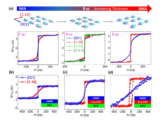
The strong octahedral tilts in La0.67Sr0.33MnO3 near interface in La0.67Sr0.33MnO3–NdGaO3 heterostructures affects the magnetic properties when the films are thin enough for the interfacial structure to dominate. In strong contrast to the normally observed easy axis along the long [10] axis Boschker et al. (2009), the easy axis of ultrathin La0.67Sr0.33MnO3 with eight unit cells is along the short [001] axis due to the interfacial magnetic anisotropy (IMA), as shown in Fig. 15a. The contribution of anisotropic strain to the magnetic anisotropy will increase with increasing thickness, hence thicker films ( eight unit cells) exhibit bulk magnetic anisotropy (BMA) with the easy axis along the [10] axis. At eight unit cells, the competition between the IMA and the BMA results in biaxial anisotropy with the easy axes along the [11] and [1] axes. The engineering of octahedral tilting by introducing an ultrathin SrTiO3 buffer layer (see Fig. 15b-d) also provides us with capabilities to switch the IMA to BMA in ultrathin LSMO films, e.g., a one unit-cell-thick SrTiO3 buffered six unit-cell-thick La0.67Sr0.33MnO3 film exhibits an easy axis along the [10] axis (see Fig. 15c). Therefore, the short impact length scale of octahedra coupling becomes a unique tool that allows us to atomically engineer octahedra rotations at the interface and thus anisotropic properties at the atomic scale.
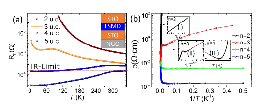
We achieved the largest reduction of the electrical dead-layer by growing La0.67Sr0.33MnO3 on SrTiO3-buffered and SrTiO3-capped NdGaO3 Liao et al. (2015), see Fig. 16. In this case a four unit-cell-thick film is still metallic and localization sets in at three unit cells. A few ingredients contribute to the reduction of the dead layer. First of all the films are under compressive strain as opposed to films grown on SrTiO3 that are under tensile strain. Compressive strain induces octahedra rotations around the out-of-plane axis whereas tensile strain induces rotations around the in-plane axes Vailionis et al. (2011). The double exchange mechanism that drives the conductivity of the manganites depends on the Mn-O-Mn bond angles; strong octahedra rotation reduces the conductivity. Therefore compressive strain promotes double exchange in the critical out-of-plane direction. Second, the adjacent SrTiO3 layers prevent the rotations from the NdGaO3 from inducing large rotations in the La0.67Sr0.33MnO3 which would be detrimental for the electrical transport. However, it could be expected that the SrTiO3 layers induce octahedra deformation just as is the case of La0.67Sr0.33MnO3 grown on SrTiO3 crystals. Judging from the reduction of the dead layer, this is not so much the case for these heterostructures. Some structural differences are present: the SrTiO3 is strained and probably has an a0a0c- tilt pattern instead of the standard cubic a0a0a0 tilt pattern and the La0.67Sr0.33MnO3is orthorhombic (a+b-c- tilt pattern) under compressive strain instead of tetragonal (a+a-c0 tilt pattern) under tensile strain. Presumably one of these structural factors together with the limited thickness of the SrTiO3 layers prevents the SrTiO3 from inducing the Jahn-Teller distorted interfacial layer that occurs in La0.67Sr0.33MnO3 grown on SrTiO3 crystals.
VII Conclusions
The magnetic dead-layer at the La0.67Sr0.33MnO3–SrTiO3 interface can be eliminated with the use of compositional interface engineering. The electrical dead-layer, however, remains present in all the heterostructures. The structural distortions induced by oxygen octahedra connectivity are likely the dominant cause for the electrical dead-layer, consistent with the conclusions of a variety of other experiments and theoretical models Pruneda et al. (2007); He et al. (2010); Gray et al. (2010); Petrov et al. (2013). Also experiments performed on (011) oriented SrTiO3 clearly indicated the importance of the oxygen octahedra rotation pattern on the functional properties Boschker et al. (2012b).
The experiments demonstrate that interface engineering is a powerful tool for studying the properties of materials at interfaces systematically. Due to the importance of the local crystal structure, a main challenge for materials engineers is the control of the amount and direction of the oxygen octahedra rotations at the interface. Next to the results shown in section VI other possible approaches to optimize La0.67Sr0.33MnO3 interfaces are using buffer layers with the right rotation patterns, changing the cation size at the interface, similar to bulk experiments in the manganites Radaelli et al. (1997), and using infinite layer compounds to eliminate the oxygen octahedra connectivity.
Acknowledgements.
The authors gratefully acknowledge key contributions to the research made by Arturas Vailionis (XRD), Sandra van Aert, Sara Bals, Ricardo Egoavil, Nicolas Gauquelin, Staf van Tendeloo and Jo Verbeeck (STEM), Valeria Lauter, Yaohua Liu and Suzanne te Velthuis (PNR) and Ramamoorthy Ramesh and Pim Rossen (TOF-MS). The transport measurements discussed in section V were performed during a stay of H.B. at the University of Tokyo and would not have been possible without the help of Chris Bell, Yasuyuki Hikita, Harold Hwang and Takeaki Yajima.References
- Lee et al. (2005) H. N. Lee, H. M. Christen, M. F. Chisholm, C. M. Rouleau, and D. H. Lowndes, NATURE 433, 395 (2005).
- Boschker et al. (2012a) H. Boschker, J. Verbeeck, R. Egoavil, S. Bals, G. van Tendeloo, M. Huijben, E. P. Houwman, G. Koster, D. H. A. Blank, and G. Rijnders, ADVANCED FUNCTIONAL MATERIALS 22, 2235 (2012a).
- Peng et al. (2014) R. Peng, H. C. Xu, M. Xia, M. Xia, J. F. Zhao, X. Xie, D. F. Xu, B. P. Xie, and D. L. Feng, APPLIED PHYSICS LETTERS 104, 081606 (2014).
- Huijben et al. (2015) M. Huijben, Y. Liu, H. Boschker, V. Lauter, R. Egoavil, J. Verbeeck, S. G. E. te Velthuis, G. Rijnders, and G. Koster, ADVANCED MATERIALS INTERFACES 2, 1400416 (2015).
- Chen et al. (2015) Y. Z. Chen, F. Trier, T. Wijnands, R. J. Green, N. Gauquelin, R. Egoavil, D. V. Christensen, G. Koster, M. Huijben, N. Bovet, S. Macke, F. He, R. Sutarto, N. H. Andersen, J. A. Sulpizio, M. Honig, G. E. D. K. Prawiroatmodjo, T. S. Jespersen, S. Linderoth, S. Ilani, J. Verbeeck, G. Van Tendeloo, G. Rijnders, G. A. Sawatzky, and N. Pryds, NATURE MATERIALS 14, 801 (2015).
- Bousquet et al. (2008) E. Bousquet, M. Dawber, N. Stucki, C. Lichtensteiger, P. Hermet, S. Gariglio, J.-M. Triscone, and P. Ghosez, NATURE 452, 732 (2008).
- Boschker et al. (2012b) H. Boschker, J. Kautz, E. P. Houwman, W. Siemons, D. H. A. Blank, M. Huijben, G. Koster, A. Vailionis, and G. Rijnders, PHYSICAL REVIEW LETTERS 109, 157207 (2012b).
- Rondinelli et al. (2012) J. M. Rondinelli, S. J. May, and J. W. Freeland, MRS BULLETIN 37, 261 (2012).
- Aso et al. (2014) R. Aso, D. Kan, Y. Shimakawa, and H. Kurata, CRYSTAL GROWTH & DESIGN 14, 2128 (2014).
- Moon et al. (2014) E. J. Moon, P. V. Balachandran, B. J. Kirby, D. J. Keavney, R. J. Sichel-Tissot, C. M. Schlepuetz, E. Karapetrova, X. M. Cheng, J. M. Rondinelli, and S. J. May, NANO LETTERS 14, 2509 (2014).
- Zhai et al. (2014) X. Zhai, L. Cheng, Y. Liu, C. M. Schlepuetz, S. Dong, H. Li, X. Zhang, S. Chu, L. Zheng, J. Zhang, A. Zhao, H. Hong, A. Bhattacharya, J. N. Eckstein, and C. Zeng, NATURE COMMUNICATIONS 5, 4283 (2014).
- Yajima et al. (2011) T. Yajima, Y. Hikita, and H. Y. Hwang, NATURE MATERIALS 10, 198 (2011).
- Driza et al. (2012) N. Driza, S. Blanco-Canosa, M. Bakr, S. Soltan, M. Khalid, L. Mustafa, K. Kawashima, G. Christiani, H.-U. Habermeier, G. Khaliullin, C. Ulrich, M. Le Tacon, and B. Keimer, NATURE MATERIALS 11, 675 (2012).
- Lee et al. (2013) C.-H. Lee, N. D. Orloff, T. Birol, Y. Zhu, V. Goian, E. Rocas, R. Haislmaier, E. Vlahos, J. A. Mundy, L. F. Kourkoutis, Y. Nie, M. D. Biegalski, J. Zhang, M. Bernhagen, N. A. Benedek, Y. Kim, J. D. Brock, R. Uecker, X. X. Xi, V. Gopalan, D. Nuzhnyy, S. Kamba, D. A. Muller, I. Takeuchi, J. C. Booth, C. J. Fennie, and D. G. Schlom, NATURE 502, 532 (2013).
- Park et al. (1998) J. H. Park, E. Vescovo, H. J. Kim, C. Kwon, R. Ramesh, and T. Venkatesan, NATURE 392, 794 (1998).
- Sun et al. (1999) J. Z. Sun, D. W. Abraham, R. A. Rao, and C. B. Eom, APPLIED PHYSICS LETTERS 74, 3017 (1999).
- Bowen et al. (2003) M. Bowen, M. Bibes, A. Barthelemy, J. P. Contour, A. Anane, Y. Lemaitre, and A. Fert, APPLIED PHYSICS LETTERS 82, 233 (2003).
- Postma et al. (2004) F. M. Postma, R. Ramaneti, T. Banerjee, H. Gokcan, E. Haq, D. H. A. Blank, R. Jansen, and J. C. Lodder, JOURNAL OF APPLIED PHYSICS 95, 7324 (2004).
- Hikita et al. (2009) Y. Hikita, M. Nishikawa, T. Yajima, and H. Y. Hwang, PHYSICAL REVIEW B 79, 073101 (2009).
- Garcia et al. (2010) V. Garcia, M. Bibes, L. Bocher, S. Valencia, F. Kronast, A. Crassous, X. Moya, S. Enouz-Vedrenne, A. Gloter, D. Imhoff, C. Deranlot, N. D. Mathur, S. Fusil, K. Bouzehouane, and A. Barthelemy, SCIENCE 327, 1106 (2010).
- Kavich et al. (2007) J. J. Kavich, M. P. Warusawithana, J. W. Freeland, P. Ryan, X. Zhai, R. H. Kodama, and J. N. Eckstein, PHYSICAL REVIEW B 76, 014410 (2007).
- Huijben et al. (2008) M. Huijben, L. W. Martin, Y. H. Chu, M. B. Holcomb, P. Yu, G. Rijnders, D. H. A. Blank, and R. Ramesh, PHYSICAL REVIEW B 78, 094413 (2008).
- Koster et al. (1998) G. Koster, B. L. Kropman, G. J. H. M. Rijnders, D. H. A. Blank, and H. Rogalla, APPLIED PHYSICS LETTERS 73, 2920 (1998).
- Ohtomo et al. (2002) A. Ohtomo, D. A. Muller, J. L. Grazul, and H. Y. Hwang, APPLIED PHYSICS LETTERS 80, 3922 (2002).
- van der Pauw (1958) L. J. van der Pauw, PHILIPS TECHNICAL REVIEW 20, 220 (1958).
- Boschker et al. (2011) H. Boschker, M. Huijben, A. Vailionis, J. Verbeeck, S. van Aert, M. Luysberg, S. Bals, G. van Tendeloo, E. P. Houwman, G. Koster, D. H. A. Blank, and G. Rijnders, JOURNAL OF PHYSICS D-APPLIED PHYSICS 44, 205001 (2011).
- Koster et al. (2000) G. Koster, G. Rijnders, D. H. A. Blank, and H. Rogalla, PHYSICA C-SUPERCONDUCTIVITY AND ITS APPLICATIONS 339, 215 (2000).
- Yu et al. (2012) P. Yu, W. Luo, D. Yi, J. X. Zhang, M. D. Rossell, C. H. Yang, L. You, G. Singh-Bhalla, S. Y. Yang, Q. He, Q. M. Ramasse, R. Erni, L. W. Martin, Y. H. Chu, S. T. Pantelides, S. J. Pennycook, and R. Ramesh, PROCEEDINGS OF THE NATIONAL ACADEMY OF SCIENCES OF THE UNITED STATES OF AMERICA 109, 9710 (2012).
- Van Aert et al. (2009) S. Van Aert, J. Verbeeck, R. Erni, S. Bals, M. Luysberg, D. Van Dyck, and G. Van Tendeloo, ULTRAMICROSCOPY 109, 1236 (2009).
- Nakagawa et al. (2006) N. Nakagawa, H. Y. Hwang, and D. A. Muller, NATURE MATERIALS 5, 204 (2006).
- Kumigashira et al. (2006) H. Kumigashira, A. Chikamatsu, R. Hashimoto, M. Oshima, T. Ohnishi, M. Lippmaa, H. Wadati, A. Fujimori, K. Ono, M. Kawasaki, and H. Koinuma, APPLIED PHYSICS LETTERS 88, 192504 (2006).
- Yamada et al. (2006) H. Yamada, M. Kawasaki, T. Lottermoser, T. Arima, and Y. Tokura, APPLIED PHYSICS LETTERS 89, 052506 (2006).
- Adamo et al. (2008) C. Adamo, X. Ke, P. Schiffer, A. Soukiassian, M. Warusawithana, L. Maritato, and D. G. Schlom, APPLIED PHYSICS LETTERS 92, 112508 (2008).
- Bhattacharya et al. (2008) A. Bhattacharya, S. J. May, S. G. E. t. Velthuis, M. Warusawithana, X. Zhai, B. Jiang, J. M. Zuo, M. R. Fitzsimmons, S. D. Bader, and J. N. Eckstein, PHYSICAL REVIEW LETTERS 100, 257203 (2008).
- Dingle et al. (1978) R. Dingle, H. L. Stormer, A. C. Gossard, and W. Wiegmann, APPLIED PHYSICS LETTERS 33, 665 (1978).
- Pruneda et al. (2007) J. M. Pruneda, V. Ferrari, R. Rurali, P. B. Littlewood, N. A. Spaldin, and E. Artacho, PHYSICAL REVIEW LETTERS 99, 226101 (2007).
- He et al. (2010) J. He, A. Borisevich, S. V. Kalinin, S. J. Pennycook, and S. T. Pantelides, PHYSICAL REVIEW LETTERS 105, 227203 (2010).
- Glazer (1972) A. M. Glazer, ACTA CRYSTALLOGRAPHICA SECTION B 28, 3384 (1972).
- Woodward (1997a) P. M. Woodward, ACTA CRYSTALLOGRAPHICA SECTION B 53, 32 (1997a).
- Woodward (1997b) P. M. Woodward, ACTA CRYSTALLOGRAPHICA SECTION B 53, 44 (1997b).
- Vailionis et al. (2011) A. Vailionis, H. Boschker, W. Siemons, E. P. Houwman, D. H. A. Blank, G. Rijnders, and G. Koster, PHYSICAL REVIEW B 83, 064101 (2011).
- Vailionis et al. (2014) A. Vailionis, H. Boschker, Z. Liao, J. R. A. Smit, G. Rijnders, M. Huijben, and G. Koster, APPLIED PHYSICS LETTERS 105, 131906 (2014).
- Gray et al. (2010) A. X. Gray, C. Papp, B. Balke, S.-H. Yang, M. Huijben, E. Rotenberg, A. Bostwick, S. Ueda, Y. Yamashita, K. Kobayashi, E. M. Gullikson, J. B. Kortright, F. M. F. de Groot, G. Rijnders, D. H. A. Blank, R. Ramesh, and C. S. Fadley, PHYSICAL REVIEW B 82, 205116 (2010).
- Gray et al. (2013) A. X. Gray, J. Minar, L. Plucinski, M. Huijben, A. Bostwick, E. Rotenberg, S. H. Yang, J. Braun, A. Winkelmann, G. Conti, D. Eiteneer, A. Rattanachata, A. A. Greer, J. Ciston, C. Ophus, G. Rijnders, D. H. A. Blank, D. Doennig, R. Pentcheva, J. B. Kortright, C. M. Schneider, H. Ebert, and C. S. Fadley, EUROPHYSICS LETTERS 104, 17004 (2013).
- Liao et al. (2016) Z. Liao, M. Huijben, Z. Zhong, N. Gauquelin, S. Macke, R. J. Green, S. Van Aert, J. Verbeeck, G. Van Tendeloo, K. Held, G. A. Sawatzky, G. Koster, and G. Rijnders, NATURE MATERIALS 15, 425 (2016).
- Boschker et al. (2009) H. Boschker, M. Mathews, E. P. Houwman, H. Nishikawa, A. Vailionis, G. Koster, G. Rijnders, and D. H. A. Blank, PHYSICAL REVIEW B 79, 214425 (2009).
- Lee and Ramakrishnan (1985) P. A. Lee and T. V. Ramakrishnan, REVIEWS OF MODERN PHYSICS 57, 287 (1985).
- Liao et al. (2015) Z. Liao, F. Li, P. Gao, L. Li, J. Guo, X. Pan, R. Jin, E. W. Plummer, and J. Zhang, PHYSICAL REVIEW B 92, 125123 (2015).
- Petrov et al. (2013) A. Y. Petrov, X. Torrelles, A. Verna, H. Xu, A. Cossaro, M. Pedio, J. Garcia-Barriocanal, G. R. Castro, and B. A. Davidson, ADVANCED MATERIALS 25, 4043 (2013).
- Radaelli et al. (1997) P. G. Radaelli, G. Iannone, M. Marezio, H. Y. Hwang, S. W. Cheong, J. D. Jorgensen, and D. N. Argyriou, PHYSICAL REVIEW B 56, 8265 (1997).