Optical and Electrical Properties of Nanostructured Metallic Electrical Contacts
Abstract
We study the optical and electrical properties of silver films with a graded thickness obtained through metallic evaporation in vacuum on a tilted substrate to evaluate their use as semitransparent electrical contacts. We measure their ellipsometric coefficients, optical transmissions and electrical conductivity for different widths, and we employ an efficient recursive method to calculate their macroscopic dielectric function, their optical properties and their microscopic electric fields. The topology of very thin films corresponds to disconnected islands, while very wide films are simply connected. For intermediate widths the film becomes semicontinuous, multiply connected, and its microscopic electric field develops hotspots at optical resonances which appear near the percolation threshold of the conducting phase, yielding large ohmic losses that increase the absorptance above that of a corresponding homogeneous film. Optimizing the thickness of the film to maximize its transmittance above the percolation threshold of the conductive phase we obtained a film with transmittance and a sheet resistance . We also analyze the observed emission frequency shift of porous silicon electroluminescent devices when Ag films are used as solid electrical contacts in replacement of electrolytic ones.
I Introduction
Transparent electric contacts are needed in a widespread variety of optoelectronic applications. Materials such as coinable metals are very good electrical conductors when compared to the conductive polymers or semiconductor materials often used for those applications,Ginley (2010) but unfortunately, they are opaque. Organic conductive materials and doped metallic oxides have been considered a good compromise, behaving as conductors at low frequency and as dielectrics at optical frequencies.Ginley (2010) Nonetheless, the properties of these semiconductor materials are defined by their chemical composition and their doping. Thus, tuning the threshold frequency at which they change behavior from conductor to dielectric is difficult. An alternative for the design of semitransparent electrical contacts is the use of nanostructured metallic-dielectric composites. Extraordinary optical transmissionGhaemi et al. (1998) in perforated metallic films with nanoperforations has been explained in terms of bulk and surface plasmons in nanostructured filmsDarmanyan and Zayats (2003) and is promising for the control of optical properties.Cai and Shalaev (2009) These systems, are composed of a metallic and a dielectric phase; one of them may be described as an array of nanometric inclusions with a given geometry. Material composition, geometry, and order, affect the optical properties of the system.Cortes et al. (2010); Mochán et al. (2010) Fabrication of nanostructured films with ordered patterns designed to tune optical properties in the visible (VIS) range requires high resolution lithography, employing interferometry of electronic beamsBrueck (2005); Martínez et al. (2009) or similar techniques. A relative simple alternative is to use random composite films.Connor et al. (2008) Unlike the metallic oxides, this kind of semitransparent contacts do not require high temperatures, are flexible, might possess low enough surface roughness for the optical range, and have a relatively low cost of production.
It is well known that the optical transmissionConnor et al. (2008) as well as the electrical resistivityMaaroof and Smith (2005) of uniform metallic thin films increase as the films becomes thinner. However, the reduction of the thickness of a film usually modifies its morphology leading to inhomogeneities. A thin enough film is made of separate islandsSeal et al. (2003) and is therefore non-conducting. Near but above the percolation threshold, while the conductive phase is connected, there appear optical resonances at which the transmittance is suppressed due to the power dissipated as Joule heat.Toranzos et al. (2010) In the present work, we employ a computationally efficient recursive formalism for the calculation of an effective dielectric response of nanostructured films when the length-scale of the inhomogeneities of the film are much smaller than the wavelength, thus neglecting retardation.Cortes et al. (2010); Mochán et al. (2010, 2016) This non-retarded recursive method (RM) is applicable Ortiz et al. (2014) to nano-textured inhomogeneities with scales up to one order of magnitude below the nominal wavelength. Analyzing the optical and electrical properties of semicontinuous Ag films with a graded thickness we have searched for an optimum film, with an adequate conductivity in the low frequency range and a relatively high transmittance in the VIS.
We also study Ag electrical contacts on porous silicon (PS) electro-luminescent devices (ELD). It is knownAG Cullis and Calcott (1997) that in metal/PS/cSi junctions under a bias voltage the injected carriers may recombine. Due to the quantum confinement within the thin Si regions in PS, direct radiative transitions with an energy larger than the bulk indirect gap become permitted, leading to electro-luminescence (EL) in the VIS range of the spectrum. Photo luminescence (PL) may also be observed if the sample is irradiated by ultraviolet (UV) light. A relation between the PL spectra with the porosity and the morphology of PS was proposed by Bessaï et al.Bessaïs et al. (1996), yielding a maximum emission at at 680nm with =0.8. Under similar preparation conditions, the PL and EL spectra are expected to be similarShi et al. (1993). EL spectra from PS excited through an electrolytic contactBillat et al. (1995) have been characterized as a function of the excitation potential and electric current, allowing the control of the emission spectra through the preparation condition. However, it has been found that the EL spectra of similarly prepared PS films samples differ when they are excited through different solid contacts. For PS with an expected porosity around 80% over doped Si with Au vacuum evaporated contacts (Au/PS/-Si/Al), a peak emission was obtained at 680.Koshida and Koyama (1992) Similarly for an ITO contactKoshida and Koyama (1992) or for an Al contact and an doped substrate (Al/PS/-Si/Al).Shi et al. (1993). Nevertheless, for an Au contact prepared by sputtering (Au/PS/-Si/Al) the EL peak shifts to 560nmR. et al. (2002). Other shifts have been reported for contacts made through the co-evaporation of Au and Ga or Sn (530nm), Au and In (455nm), and Au and Sb (700nm).Steiner et al. (1996) In the above cases the intensity of the EL signal was strongly suppressed.
In this paper we also explore experimentally and theoretically the spectral shift and the intensity suppression of the EL signal when an electrolytic contact over an PS-ELD is replaced by a solid Ag contact.
The paper is organized as follows: In section II we present our method for fabricating Ag films with variable thickness in only one evaporation step (subsection II.1), and we discuss our procedures for measuring the transmittance, ellipsometric coefficients and resistance ( II.2). In section III we discuss our model for the semicontinuous film and we describe our computational procedures. In section IV we obtain theoretical results from the RM for the ellipsometric coefficients (IV.1), the electrical properties(IV.2), and the transmittance (IV.3) of semicontinuous films. As an application, in section V we fabricate an optimally tuned solid transparent electrical contact (V.1) and we propose an explanation for the spectral shift and the suppression of the observed emission of a PS-ELD (subsec. V.2). We devote section VI to conclusions.
II Experimental
In this section we describe the experimental setup employed to determine the optimal thickness of thin metallic films by fabricating samples with a graded thickness and measuring their optical transmittance, ellipsometric coefficients, and four-point electrical resistance. The optimal thickness would be the one that maximizes the transmittance and minimizes the resistance.
II.1 Sample Preparation
Fig.1 displays our setup for growing film samples with a graded thickness (), adapted from a coinable-metal vacuum evaporation technique.Martin (2010); Bunshah (1994)
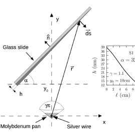
The sample is obtained by isotropic thermal evaporation of Ag through a solid angle determined by the aperture of a conical molybdenum crucible whose walls screen the lower part of a vacuum bell device. On a surface element at position on a glass slide, the deposited mass is given by where is the total Ag mass vaporized. A nominal width may be obtained by dividing the mass per unit area of the film by the bulk mass density of Ag. The actual density may be smaller and the actual width larger due to texture of the film. Due to the inclination of the slide with respect to the horizontal, the deposited film is thicker on the side that is closer to the source, at a height above the crucible, and thinner on the opposite side. Thus, we can prepare samples with variable thickness within a range that depends on the geometrical parameters of the experimental setup. We show below results for two samples, both prepared with , sample with 10 cm, , mg and sample with 9.7 cm, , and mg. The inset of Fig.1 shows the thickness as a function of position along the sample .
II.2 Optical and electrical properties
We measured and averaged the optical normal-incidence transmittance along three parallel equispaced lines running longitudinally through the sample in the gradient direction, using (a) a 650 nm diode laser with a spot of diameter 1.5 mm, and (b) an Ocean Optics UV-NIS-NIR source through an optical fiber. In both cases we measured the intensity of the transmitted light at mm intervals. We used a clean glass slide as a reference. For (a) we used a detector based on a photo-diode BPW20RF and in (b) the data were collected from a USB spectrometer and we employed the Spectrasuite software. We also determined the sheet resistance over the same places using a four-point technique.Martin (2010); Cohen (1983)
We measured the ellipsometric parameters of the sample and , defined through
| (1) |
where and are the reflection coefficients for and polarization, respectively, with a Rudoph Research type 43702-200E ellipsometer in the null field mode.Zerbino et al. (2007) We fixed the incidence angle , we put a linear polarizer and a quarter wave plate across the incident beam oriented at angles and with respect to the plane of incidence, respectively, and a linear analyzer across the reflected beam at an angle . We set and found , and for different film thicknesses and wavelengths, where we choose and to minimize the intensity of the outgoing beam.
III Model
For very thin films of coinable metals an island morphology type has been reported.Maaroof and Smith (2005); Cai and Shalaev (2009) As the film grows the islands eventually connect among themselves, leading to a semicontinuous film textured in the nanometric scale.Bishop (2007); Maaroof and Smith (2005); Seal et al. (2003) For thickness smaller than a couple dozen nanometers, the air interstices among the islands may sustain resonant excitations that significantly modify the opticalCortes et al. (2010); Mochán et al. (2010) and electricalOrtiz et al. (2010) properties. As we move along our graded sample towards its thick edge those islands become more connected and for very thick films they merge into a continuous film.
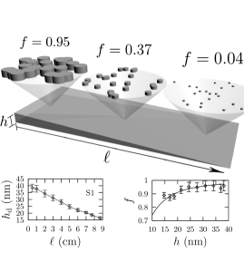
Fig. 2 shows schematically the proposed morphology. Our model consists of an ensemble of periodically repeated unit cells, each of which contains a large enough number of penetrable disks of radius and height occupying random uncorrelated positions. The ensemble is characterized by the filling fraction , i.e., the fraction of the area covered by the metal, and the amount of metal deposited per unit area, which in turn is characterized by the nominal height . We employed the RM to calculate the macroscopic dielectric function of the compositeCortes et al. (2010); Mochán et al. (2010); Ortiz et al. (2014) using the Photonic package.Mochán et al. (2016) The filling fraction may be adjusted in the model by varying the radius of the disks and the height is related to through .
IV Results
IV.1 Ellipsometric coefficients
We measured the ellipsometric coefficients at a fixed incidence angle . We measured and at ten different positions along sample and five wavelenghts 405, 451, 492, 546 and 580nm. In the left panel of Fig. 3 we show our results for three of those (we omitted two to avoid cluttering the figure).
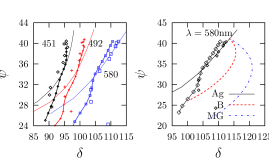
Each point in Fig. 3 corresponds to a different thickness ( increases with ). For thick films (above 20 nm) experiment agrees roughly with the values of and calculated for a locally homogeneous film of width with a dielectric function taken from Ref. Johnson and Christy, 1972 (commonly used for studying optical properties of Ag composites at frequencies in UV-VIS-NIR range) and deposited over glass, with dielectric response obtained from Ref. E.D.Palik, 1985, but they don’t agree for thinner films (nm) for which the film inhomogeneities lead to a strong dependency of the optical response with the film morphology. For each value of and we used our model (Subsec. III) to obtain the macroscopic response of the film and identifying the width of the film with the height of the disks we calculated the ellipsometric coefficients. To this end we averaged our results over a thousand realizations of our ensemble with thirty disks randomly situated within a square unit cell. We have verified convergence of the results. Our model has only one parameter, namely, the radius of the disks, and it is adjusted for each value of with corresponding nominal width , to best reproduce the ellipsometric measurements at the five wavelengths mentioned above. Fig. 2 displays the fitted values of at the ten positions for which we measured and . It also displays the resulting filling fraction as a function of the nominal height , together with an analytical fit, for which we chose the form
| (2) |
as it is linear for thin films and saturates at for very thick ones. We obtained the parameter .
The left panel of Fig. 3 shows that results of our RM calculation agree with experiment for most of the film thicknesses explored. In contrast, the effective medium models of Maxwell-Garnett (MG) and Bruggeman (B)Garland and Tanner (1978) differ strongly, as shown in the right panel of Fig. 3 corresponding to 580nm. Thus, our model system and the RM computational procedure are much better suited for the calculation of the effects of the nanometric texture on optical properties of very thin films. It has been reportedSeal et al. (2003); Maaroof and Smith (2005) that optical properties of inhomogeneous films (such as semicontinuous film of coinable metals) differ from those of homogeneous films. However, to our knowledge, this is the first time that semicontinuous Ag films are analyzed and that the differences between homogeneous and inhomogeneous films are calculated and compared to those measured on a single sample consisting of a film with a graded thickness. This kind of analysis allows correlation of the parameters needed to design and manufacture semicontinuous films with optimal parameters.
IV.2 Resistance
In Fig. 4 we show our measurements of the sheet resistance at various positions on sample , prepared with a larger angle and a smaller mass than sample , so that for each position the corresponding film is thinner. We also show the filling fraction calculated for each , using Eq. (2) (fitted to the ellipsometric parameters of sample ) and using the nominal height as a function of as described in Subsec. II.1. Notice that the resistance increases very fast as increases, the film becomes thinner, and the filling fraction of the metal diminishes, indicative of the approach to a percolation transition at where the resistance would diverge (we couldn’t measure the resistance for filling fractions smaller than ). In sample this region corresponds roughly to the center of the sample, whereas in sample it is too close to one of its edges, difficulting its measurement.

From the filling fraction and the nominal height we obtained the height of our model disks. This allows us to calculate the resistivity
| (3) |
and the sheet resistance using the RM model. To that end, we extrapolate the dielectric function of the metallic phase towards low frequencies using the Drude model
| (4) |
with parameters eV,Cai and Shalaev (2009) eV, which correspond to the resistivity cm which we measured for the same Ag wire from which the samples were prepared.
The theoretical results are displayed in Fig. 4. Notice that they also increase rapidly as increases, though not as rapidly as experiment. We recall that the geometrical percolation threshold for penetrable disks is Quintanilla et al. (2000) and that our calculations are done on a system made up of a periodically repeated finite random unit cell so that we expect finite size effects to wash away the percolation transition in our calculation. In the same figure we also include the sheet resistance of a continuous film. Its behavior is qualitatively different from both experiment and our calculation. Of course, for small and high filling fractions both models coincide and agree with experiment.
IV.3 Transmittance
Fig. 5 displays the transmittance normalized to the transmittance of the glass slide as function of position , and thus, as a function of the filling fraction , measured at =650 nm for sample . We also show the transmittance calculated with the RM model and the result for a homogeneous film.
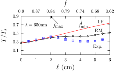
As increases and decreases the experimental transmittance increases up to a local maximum corresponding to a filling fraction for which the film is conducting as it lies above the percolation threshold displayed in Fig. 4. Afterwards, diminishes and reaches a local minimum at . As the filling fraction diminishes further, the transmittance of the film increases again, but for the film is no longer conducting. The RM calculation does not show the maximum and minimum discussed above, but displays a similar inflection, and it follows the experimental results much more closely than the calculation for a homogeneous film.
The optical properties close to the percolation threshold depend strongly on the morphology and on the wavelength. In this region field fluctuations are very intense and localized optical resonances known as hotspots occur.
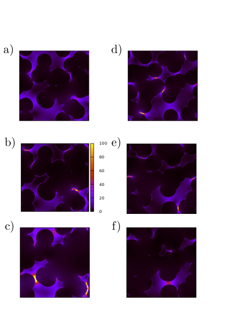
To illustrate the hotspots, in Fig. 6 we show the microscopic field obtained through a recursive procedure based in the RM calculation of the response.Mochán et al. (2015, 2016) We show the field for two different members of the random ensemble that models the morphology of the system, and for three disk radii , 0.12, 0.13, corresponding to the averaged filling fractions , 0.75, 0.81, at a single wavelength nm. Fig.6c) displays hotspots in the interstice between two nearby particles (bottom left) and between three particles (bottom right), in which is approximately 2 orders of magnitude larger than its mean value. Similar hotspots appear at different positions for different wavelengths and for different filling fractions, as illustrated by the other panels of the figure. Fig.6b) shows four different hotspots for a slightly smaller . With even smaller Fig.6a) shows no hotspots. But, another member of the ensemble ensemble with the same displays several as exemplified by Fig.6d). The set of hotspots for that member also change position and intensity as grows (Figs. 6e and 6f). There are well known results on the scaling of the localized states for disordered randomShalaev (1996); Markel et al. (1999) and fractalM.I.Stockman et al. (1996); Ortiz and Mochán (2003) systems. These localized states have found applications due to the corresponding enhancement in linear and nonlinear signals. For example, SERS and KERS enhancements of 1 to 2 dozen order of magnitude have been reported.Moskovits (1985); Sarychev and Shalaev (2000)
The presence of hotspots in the microscopic field for filling fractions around the percolation threshold is responsible for an increased energy absorption within the conducting film, and thus to the decrease in the transmittance as compared to that of a homogeneous film, as seen in Fig.5 for . This energy absorption corresponds to Joule heat that is related to the imaginary part of . Fig.7 displays the real and imaginary parts of the ensemble average of as a function of the filling fraction and of the wavelength.
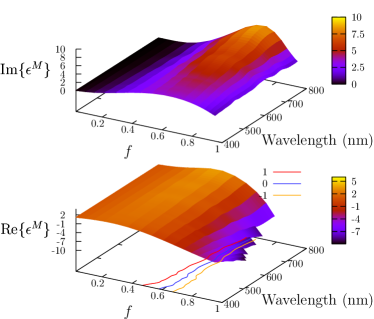
For , , } is relatively small and . Thus, the index of refraction is close to an imaginary number, the film is opaque and the field decays across it by a factor . Therefore, as increases and decreases the transmittance increases. As decreases further, becomes less negative and the field penetrates more into the film. Nevertheless, also increases and reaches a maximum for , thus increasing the absorption and decreasing the transmittance. For even larger and smaller the film becomes dielectric and the transmittance increases again. This explains qualitatively the maximum and minimum transmittance observed in Fig. 5. The corresponding inflection in the transmittance is reproduced by our numerical calculation, although not the actual maximum and minimum.
V Applications
V.1 Optimization of semicontinuous Ag film
An optimal transparent electrical contact would have the highest possible transmittance and the lowest possible resistance. To choose the best combination of parameters we plot as a function of in Fig. 8, combining information from Figs. 4 and 5.
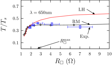
It is clear that it is not useful to diminish the nominal width of the film too much, as the transmittance stops increasing while the resistance does. Thus, an optimal choice would correspond to the maximum transmittance which corresponds to , , cm, , nm, nm
V.2 Electro-luminescence of PS with an Ag contact
We analyze light emitting devices (LED) made of porous silicon (PS) over which Ag is sputtered to form an electrical contact. We prepare the PS sample by anodizing a crystalline -doped Si substrate with resistivity 0.5-1.0cm terminated in a (100) surface, using a well known procedure:Ossicini et al. (2003) We immerse the Si crystal in an electrolytic solution of hydrofluoric acid, distilled water, and ethanol in proportions 1:1:2 and we apply a current with a density of 20 mA/cm2 for a duration of 120 sToranzos et al. (2010) to obtain a sample with an expected porosity . We discard the electrolytic solution and clean the system with an ethanol bath.
If we use a diluted solution of potassium chloride as an electrolytic contact and apply a forward current with density 16 mA/cm2 an electroluminescent signal is produced. We measured the normalized spectral emission with an Hitachi fluorimeter F2000 with blocked excitation source s after turning the current onToranzos et al. (2008). The results are displayed in Fig. 9
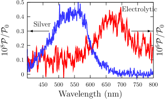
It is well known that luminescence of PSBuda et al. (1992) is due to the confinement of charge carriers within the pore walls, which introduces an uncertainty in the momentum that allows direct transitions that would be forbidden in bulk Si.Kovalev et al. (1999) Thus, the indirect gap of bulk Si gives rise to a direct electronic transition in PS that is shifted due to quantum confinement and corresponds to the emitted emission with wavelength nm illustrated by the peak on the right of Fig.9 corresponding to an electrolytic contact.Steiner et al. (1996) While the current flows, silicon oxide is progressively produced on the walls of the pores, increasing the confinement and producing a small blue shift of the maximum emission peak.Ossicini et al. (2003) After the current had been applied for approximately s the electroluminiscence of our sample was extinguished.
The electrical excitation of PS may also be realized with Schottky type metallic solid contacts.Steiner et al. (1996) An advantage of metallic contacts is that the electric current doesn’t produce the chemical reactions that rapidly destroys the electroluminiscence when an electrolytic contact is employed, extending the life of the device. To produce a metallic contact, we use cathodic projection (sputtering) of Ag on a masked surface of a PS sample fabricated as described above. We chose the sputtering conditions (pressure, arc current, distance of Ag target to sample, deposition time) by first sputtering onto a glass sample and selecting those conditions that yielded a film with relative transmittance .
Fig. 9 shows the electroluminiscence spectrum of our sample with a metallic contact excited by an electric current with density density of 20 mA/cm2. Comparing this spectrum with that corresponding to the electrolytic contact, we notice that it is strongly blue-shifted towards the central part of VIS spectra ( 550nm), but that its intensity is about two orders of magnitude smaller.
To understand the shift of the maximum of the emission spectra from for an electrolytic contact to for an Ag contact, we obtained the emission spectra from the photo-luminescence (PL) spectra of Si nano-crystals and their size dependence.Kovalev et al. (1999) The effects of confinement in the walls of PS have been related to the effects of confinement in nano-crystals and a relation between porosity and effective size has been proposed,Bessaïs et al. (1996) as well as analytical expressions for the shift of the emission peak with respect to size.Fauchet and von Behren (1997) If the sample is kept in air there is a further blue shift due to oxidation at the surface of the pores.R. et al. (2002); Steiner et al. (1996) Thus, we model the intrinsic PL spectrum of PS as a Gaussian of an appropriate width centered at the energy corresponding to the porosity, and we assume that the EL emission spectrum is similar to the PL one. In the top panel of Fig.10 we show the resulting PL spectra as a function of both wavelength and porosity.Ossicini et al. (2003).
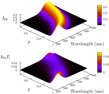
When using a solid contact, the light produced through EL is transmitted through the contact before being observed. Thus we expect that the observed EL signal should be given by the product of the emission, similar to the the PL spectrum, and the optical transmittance of the system PS/contact/air. We model the contact by assuming most of the metal infiltrates the pores. We used the RM method to calculate the macroscopic dielectric response of PS modeled as a random ensemble of empty cylinders within a crystalline Si host of porosity ,Ortiz et al. (2010) and we also use the RM method to calculate the macroscopic dielectric response of the contact modeled as a random ensemble of Ag cylinders within the crystalline Si host, with a filling fraction given by the porosity. We calculate the transmittance of the system formed by PS covered with a film of width made up of Ag-infiltrated PS. In Fig.10 we also show the product of the intrinsic PS luminescence signal with the transmittance for nm. Notice that the signal is suppressed about two orders of magnitude with respect to the PL spectrum and that it is becomes blue shifted and more intense as the porosity increases.
Finally, we assume that the porosity in our random sample is not fixed at the nominal value % expected from our preparation procedure, but has some fluctuations. We assume is distributed as a Gaussian of width around its average and. In Fig. 11 we show the corresponding EL spectra for different thicknesses of the contact.
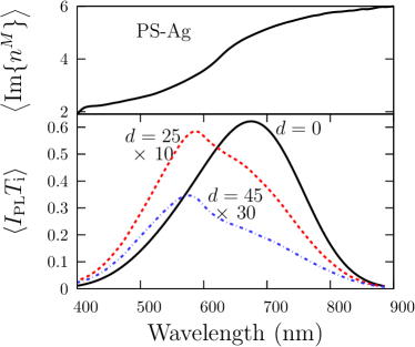
The curve for corresponds to the absence of metal, and thus may be compared to the EL spectrum with a transparent electrolytic contact. It has a peak at 680 nm which agrees well with that in the right side of Fig. 9. The peak is slightly red shifted with respect to the nominal peak corresponding to in the top panel of Fig. 10, as the direction of its ridge is closer to that of the axis for lower frequencies.
On the other hand, the peaks of the curves corresponding to nm and nm are blue shifted to 590nm and 570nm and are suppressed about one and two orders of magnitude respectively. The reason for the shift and the height decrease of the peaks lies in the absorption within the contact, as illustrated in the top panel of Fig. 11, which shows that the macroscopic index of refraction of the contact is large and increases with wavelength, therefore yielding a stronger suppression at the red end of the spectrum. Thus, our model of a metallic contact that partially infiltrates the pores PS is able to explain blue shift and suppression of the EL spectra observed experimentally and illustrated by the curve on the left side of Fig. 9. On the other hand, we were unable to reproduce the experimental results using a metallic semicontinuous overlayer, as in the previous sections, as a contact. Our results are not very sensitive to the width of the porosity distribution, but we don’t get a large enough shift in the limit .
VI Conclusions
We prepared Ag thin films with a height gradient by evaporation onto a tilted glass substrate. We performed ellipsometric measurements which showed than the films changed nature from locally homogeneous to semicontinuous and to an island morphology as their width diminished. We modeled the system as an ensemble of penetrable metallic cylinders occupying random uncorrelated positions, and we applied an efficient recursive formalism to obtain its macroscopic dielectric function. We fitted the ellipsometric measurements to relate the position along the sample film and the nominal height of the film to its actual height and its (area) filling fraction. We measured and analyzed with the previous fit the sheet resistance of the film and identified a percolation transition where the film resistance along the film diverges. The optical transmittance of the film was also measured and analyzed, and we obtained a deviation from the transmittance of a homogeneous film. As the film becomes narrower the transmittance increases, reaches a maximum and then it decreases until it hits a minimum and increases again, but this time as a dielectric and not a conducting film. This behavior has been attributed to the scattering of light by the inhomogeneities of the filmBishop (2007). Nevertheless, these inhomogeneities are not expected to have a lengthscale much larger than the height of the film, much smaller than the wavelength of light, so that scattering is expected to be smallBohren and Huffman (1983) and the film may be characterized by a macroscopic effective permittivity.Ortiz et al. (2014) Our model calculation of the dielectric response captured qualitatively the behavior of the transmittance, although with smaller oscillations as the filling fraction decreases, displaying an inflection, but without an actual maximum and a minimum. We explained qualitatively the behavior of the transmittance in terms of plasmonic resonances within the film. For a range of filling fractions around the percolation threshold a series of resonances appear for which the field becomes very intense in very small regions. These hotspots are responsible for an increased energy dissipation within the film, as shown by an the imaginary part of the macroscopic dielectric function of the system. We employed our results to optimize a film for use as a semitransparent contact. We also calculated the shift towards the blue and the decrease in the intensity of the electro-luminescence of porous silicon when a metallic semicontinuous contact is employed instead of an electrolytic one, and obtained agreement with experiment assuming that the metal infiltrates the pores and that the porosity has some fluctuations around its mean.
Acknowledgment
We acknowledge support from ANPCyT/FONCyT and UNNE through the grants PICT/2013-0696, PI-F008/2014-SGCyT, and from DGAPA-UNAM through grant No. IN113016.
References
- Ginley (2010) D. S. Ginley, Handbook of Transparent Conductors (Springer, USA, 2010).
- Ghaemi et al. (1998) H. Ghaemi, T. Thio, D. Grupp, T. Ebbesen, and H. Lezec, Phys. Rev. B 58, 6779 (1998).
- Darmanyan and Zayats (2003) S. Darmanyan and A. Zayats, Phys. Rev. B 67, 035424 (2003).
- Cai and Shalaev (2009) W. Cai and V. Shalaev, Optical Metamaterials: Fundamentals and Applications (Springer, New York, 2009).
- Cortes et al. (2010) E. Cortes, W. L. Mochán, B. S. Mendoza, and G. P. Ortiz, Phys. Stat. Sol. B 247, 2102 (2010).
- Mochán et al. (2010) W. L. Mochán, G. P. Ortiz, and B. S. Mendoza, Opt. Express 18, 22119 (2010).
- Brueck (2005) S. Brueck, Proc. IEEE 93, 1704 (2005).
- Martínez et al. (2009) E. Martínez, M. Bellino, and G. Soler-Illia, ACS applied materials & interfaces 1, 746 (2009).
- Connor et al. (2008) B. O. Connor, C. Haughn, K. An, K. Pipe, and M. Shtein, Appl. Phys. Lett 93, 223304 (2008).
- Maaroof and Smith (2005) A. I. Maaroof and G. B. Smith, Thin Solid Films 485, 198 (2005).
- Seal et al. (2003) K. Seal, M. A. Nelson, and Z. C. Ying, Phys. Rev. B 67, 035318 (2003).
- Toranzos et al. (2010) V. Toranzos, G. Ortiz, and R. Koropecki, in ANALES AFA, Vol. 22 (Asociación Física Argentina, 2010) pp. 37–41.
- Mochán et al. (2016) W. L. Mochán, G. Ortiz, B. S. Mendoza, and J. S. Pérez-Huerta, “Photonic,” Comprehensive Perl Archive Network (CPAN) (2016), perl package for calculations on metamaterials and photonic structures.
- Ortiz et al. (2014) G. Ortiz, M. Inchaussandague, D. Skigin, R. Depine, and W. L. Mochán, Journal of Optics 16, 105012 (2014).
- AG Cullis and Calcott (1997) L. C. AG Cullis and P. Calcott, J App Phys 82, 909 (1997).
- Bessaïs et al. (1996) B. Bessaïs, H. Ezzaouia, H. Elhouichet, M. Oueslati, and R. Bennaceur, Semicond. Sci. Technol. 11, 1815–1820 (1996).
- Shi et al. (1993) H. Shi, Y. Zheng, Y. Wang, and R. Yuan, Appl. Phys. Lett. 63, 770 (1993).
- Billat et al. (1995) S. Billat, F. Gaspard, R. Hérino, M. Ligeon, F. Muller, F. Romestain, and J. Vial, Thin Solid Films 263, 238 (1995).
- Koshida and Koyama (1992) N. Koshida and H. Koyama, Appl. Phys. Lett 60, 347 (1992).
- R. et al. (2002) G. R., R.Peña-Sierra, and G. Castillo-Cabrera, Rev. Mex. Fis. 48, 92 (2002).
- Steiner et al. (1996) P. Steiner, A. Wiedenhofer, F. Kozlowski, and W. Lang, Thin Solid Films 276, 159 (1996).
- Martin (2010) P. M. Martin, Handbook of Deposition Technologies for Films and Coatings: Science, Applications and Technology (Elsevier, USA, 2010) p. 740.
- Bunshah (1994) R. F. Bunshah, Handbook of Deposition Technologies for Films and Coatings: Science, Applications and Technology (Noyes Publications, USA, 1994).
- Cohen (1983) S. S. Cohen, Thin Solid Films 104, 361 (1983).
- Zerbino et al. (2007) J. Zerbino, L. Pesetti, and M. Sustersic, J. Mol. Liquids 131-132, 185 (2007).
- Bishop (2007) C. A. Bishop, Vacuum Deposition Onto Webs, Films, and Foils (Willian Andrew, New York, 2007).
- Ortiz et al. (2010) G. Ortiz, L. Valdez, G. López, B. Mendoza, and W. Mochán, ANALES AFA 22 (2010).
- Johnson and Christy (1972) P. B. Johnson and R. M. Christy, Phys. Rev. B 6, 4370 (1972).
- E.D.Palik (1985) E.D.Palik, ed., Handbook of optical constants of solids, Academic press handbook series (Academic, Orlando, Florida., 1985).
- Garland and Tanner (1978) J. C. Garland and D. B. Tanner, eds., AIP Conference Proceeding, AIP Conference Proceeding No. 40 (American Institute of Physics, New York, 1978).
- Quintanilla et al. (2000) J. Quintanilla, S. Torquato, and R. M. Ziff, J. Phys. A: Math. Gen 33, L399 (2000).
- Mochán et al. (2015) W. L. Mochán, B. S. Mendoza, and G. P. Ortiz, in Memorias del VI Taller sobre Metamateriales, Cristales Fotónicos, Cristales Fonónicos y Estructuras Plasmónicas (UNISON, Hermosillo, feb. 2016, San Miguel de Allende, 2015) pp. 12–14.
- Shalaev (1996) V. Shalaev, Physics Reports 272, 61 (1996).
- Markel et al. (1999) V. Markel, V. Shalaev, P. Zhang, W. Huynh, L.Tay, T. Haslett, and M. Moskovits, Phys. Rev. B. 59, 10903 (1999).
- M.I.Stockman et al. (1996) M.I.Stockman, L.N.Pandey, and T.F.George, Phys. Rev. B 53, 2183 (1996).
- Ortiz and Mochán (2003) G. Ortiz and W. Mochán, Phys. Rev. B. 67 (2003).
- Moskovits (1985) M. Moskovits, Rev. Mod. Phys. 5, 783 (1985).
- Sarychev and Shalaev (2000) A. Sarychev and V. Shalaev, Physics Reports 335, 275 (2000).
- Ossicini et al. (2003) S. Ossicini, L. Pavesi, and F. Priolo, Light Emiting Silicon For Microphotonics, Vol. 194 (Springer, 2003).
- Toranzos et al. (2008) V. Toranzos, R. Koropecki, R. Urteaga, and G. Ortiz, ANALES AFA 20, 115 (2008).
- Buda et al. (1992) F. Buda, J. Kohanoff, and M. Parrinello, Phys. Rev. Lett. 69, 1272 (1992).
- Kovalev et al. (1999) D. Kovalev, H. Heckler, G. Polisski, and F. Koch, Phys. Stat. Sol. B 215, 871 (1999).
- Fauchet and von Behren (1997) P. Fauchet and J. von Behren, Phys. Stat. Sol. B 204, R7 (1997).
- Bohren and Huffman (1983) C. F. Bohren and D. R. Huffman, Absorption and Scattering of light by small particles (John Wiley and Sons, Inc., 1983).