Graphical Analysis of Current-Voltage Characteristics in Typical Memristive Interfaces
Abstract
A graphical representation based on the isothermal current-voltage (IV) measurements of typical memristive interfaces is presented. This is the starting point to extract relevant microscopic information of the parameters that control the electrical properties of a device based on a particular metal-oxide interface. The convenience of the method is illustrated presenting some examples were the IV characteristics were simulated in order to gain insight on the influence of the fitting parameters.
pacs:
73.40.-c, 73.40.Ns, 74.72.-hI Introduction
The study of the current-voltage (IV) characteristics can be a very useful tool to understand which are the microscopic factors that determine the main conduction mechanism through a metal-oxide interfaces of a device. Sze06 ; Chiu14 This microscopic knowledge may be a route to improve their capacities and a clever way to modify some specific properties. In the particular case of memristors or devices based on the resistive switching (RS) properties Waser07 ; Strukov08 ; Sawa08 , which give rise to non-volatile memories called Resistive Random Access Memories (RRAM), to understand if the resistance state (high or low) depends on electrode’s or bulk’s microscopic properties is an essential task in order to design their functionalities. In the case of the electrode-limited devices, the work function of the metal, the carrier affinity and the thickness of the oxide determine the barrier height and the probability to produce an electric-field-induced-current through the junction. The conduction mechanism can then be described as Schottky (Sch), Fowler-Nordheim (FN) or as direct tunneling emission. While in the case of bulk-limited interfaces the conduction mechanism is determined by the electrical properties of the oxide near the interface as, for example, those imposed by the existence of traps and their energy levels. Two examples of transport mechanisms influenced by the energy distribution and density of traps are the Poole-Frenkel emission (P-F) and the space-charge-limited conduction (SCLC). As an example of a device based on an electric-field-trap-controlled SCLC mechanism we can mention Ag/La0.7Ca0.3MnO3-δ interfaces Shang06 , while Au/YBa2Cu3O7-δ interfaces show a PF conduction in a variable-range hopping scenario, with a pulse-controlled-trap energy level that determines their resistance switching properties. Schulman15
In this way, different scenarios can be considered to explain the microscopic origin of the resistance change of the device, related to the particular choice of materials for the metal/oxide interface. As shown previously Sze06 ; Chiu14 , by using their isothermal IV characteristics that it is possible to distinguish if the conduction of the device is related to an ohmic behavior (), or a space charge limited conduction (SCLC, ), or a Poole-Frenkel (PF), Fowler-Nordheim (FN) or Schottky (Sch) emissions []. A simple way to enlighten the origin of the main conduction mechanism of a device is to plot as a function of the power exponent parameter , defined as , instead of trying to fit by trail and error their IV characteristics. Bozhko02 This is because the typical conduction mechanisms through metal-oxide interfaces have a simple vs curve (see Fig. 1): a pure ohmic, a Langmuir-Child (L-Ch) or a SCLC conduction will show a constant ( 1, 1.5 or 2, respectively), and a Schottky (Sch) or a Poole-Frenkel (PF) behavior will be represented by a straight line, only differing in the intercept (0 for Sch, 1 for PF). Sze06
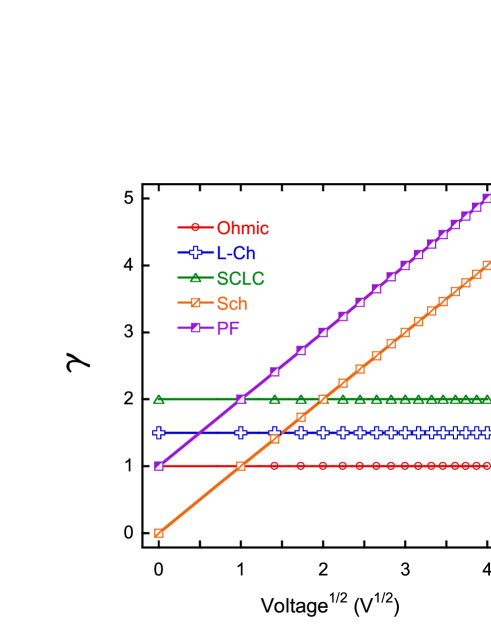
The use of this power exponent representation has proved to be convenient for extracting physical parameters in the case of non-ideal diodes. Mikhe99 Here, we show that if a combination of conducting mechanism are present in a particular metal-oxide interface, this representation would be very useful to graphically determine what they are. Otherwise, the standard way to do it will require to analyze the qualities of the fits to the IV characteristics of multiple expressions to test. It should be noted that a good fit of the IV characteristics, which includes all the participating mechanisms, is essential in order to extract a flawless microscopic description of the physics behind these devices.
By considering previous works Acha11 ; Marlasca13 ; Acha16 , the combination of conduction mechanism seems to be a common feature of bipolar memristive interfaces, as a non-linear element in parallel and/or in series with an ohmic resistance gives a convenient representation. The physical explanation of the microscopic origin of the parallel and the series structure is not clear yet. We may speculate that it can be a consequence of their capacitor-like structure where both a phase-separated interfacial zone and the proper oxide have a relevant participation in the conducting process. The interfacial zone would be composed by a mixture of conducting and insulating regions Lunkenheimer02 ; Schulman15 ; Acha16 , probably associated with a disordered distribution of oxygen vacancies (phase separation), leading to the existence of a non-linear element in parallel with an ohmic one. The series ohmic element would then represent the bulk contribution of the oxide.
II The power exponent representation
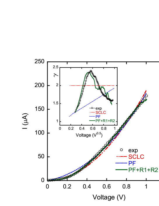
The convenience of the representation can be illustrated by the example shown in Fig. 2, corresponding to a typical IV characteristic of a Ag-La0.7Sr0.3CoO3 interface. Experimental details of the samples, the experimental setup and the way the measurements were performed can be found elsewhere. Acha16 A Sch mechanism can be ruled out as non rectifying behavior was observed: although not shown here, there was no appreciable difference in the behavior of the data when comparing between the negative and the positive quadrant.
The IV characteristics were fitted using the expressions of pure PF and SCLC conduction mechanisms Sze06 ; Chiu14 (see the solid lines in Fig. 2). Fits are not good and a combination of conduction mechanism should be considered to give a right representation of the data. At this point, the way to determine which are the relevant conducting processes is somehow tedious as it requires to fit the IV data considering, by trial and error, each possible combination of the electrical conduction processes (PF or SCLC and an ohmic resistance in parallel, or with an ohmic resistance in series, or with both of them). Hopefully, the representation of the experimental data gives a quick graphical solution to determine the specific mechanism involved, as can be observed in the inset of Fig. 2. The representation of the pure PF and SCLC conduction mechanism are clearly far from the experimental data. As we will show later, the existence of a cusp with values of with the tendency to reach an asymptotic value of 1 both in the low and high voltage regions are clear evidences of a PF conduction in parallel with an ohmic element, both in series with a second ohmic element. Then, as also shown in Fig. 2, the IV experimental data was nicely fitted with the corresponding mathematical expression to those processes. It can be seen that the representation of the fitting data also follows the experimental curve. In the next section we will discuss in detail how the representation differs in some selected examples.
II.1 Circuit representation for bipolar memristors
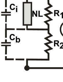
In order to gain insight into the representation, we propose to analyze the IV characteristics of the circuit elements shown in Fig. 3. The interfacial resistance is simulated by a non-linear element (NL) in parallel with an ohmic resistance . The NL element can be based on the large variety of conduction mechanism through a metal-oxide interface described in the previous section. Here, we will analyze two particular cases of NL element (SCLC and PF) which are common for bipolar memristors although the same analysis can be extended for devices dominated by a Sch conduction. The capacitance of this zone, related to the dielectric constant of the interface Lunkenheimer02 , was not considered here, as we are focusing our description on the low frequency regime. Other circuit representations of memristors can be found elsewhere. Blasco14 ; Blasco15 ; Radwan15 ; Vourkas16 The convenience of this circuit to describe the behavior of memristive interfaces was tested by reproducing the dynamical behavior of metal-YBCO interfaces Acha11 as well as by capturing the non-trivial IV characteristics of metal-manganite junctions Marlasca13 . In the case of devices with non-negligible bulk resistance, a second ohmic element in series () should be considered.
II.2 The SCLC mechanism as NL element
We first analyze the simple case of an SCLC element without traps (Child’s law) Mark62 in parallel with an ohmic resistance . In this case the current () dependence on applied voltage () corresponds to the following equation:
| (1) |
with , where is the carrier mobility, the static dielectric constant and the distance between contacts.
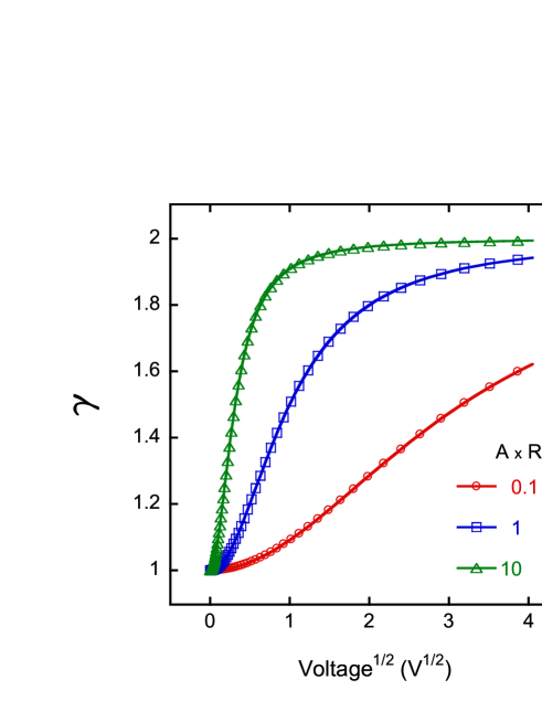
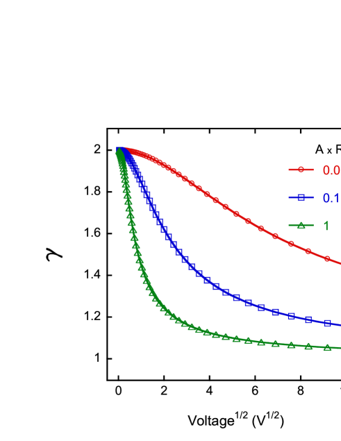
As shown in Fig 4, increases asymptotically from 1 to 2 depending on the x factor. The saturation to 2 is obtained at lower voltages when increasing this factor.
Secondly, we consider the SCLC element only in series with the ohmic element . In this case the current is related to the total voltage drop by
| (2) |
This second degree equation can be solved to extract the relation between I and V in order to calculate the factor. As shown in Fig. 5, evolves from the pure SCLC value 2 at low voltages to the ohmic dependence 1 at higher voltages. The velocity of this evolution increases when increasing the x factor.
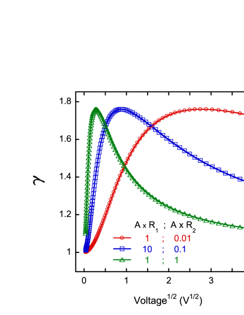
Finally, when both and are present, the relation between I and V is also obtained by solving the Eq. 3. A superposition of both previous behaviors can be observed in Fig. 6. Here, the x controls the voltage where the peak is obtained (always with ), while x determines the rapidity to tend to an ohmic behavior when increasing the voltage.
| (3) |
II.3 The PF mechanism as NL element
When dealing with a NL element related to a PF mechanism in a circuit that includes both and (see Fig. 3), the relation between the current and the voltage corresponds to the following implicit equation:
| (4) |
with
| (5) |
where is the temperature, the Boltzmann constant, the trap energy level, the electron’s charge, the conducting area, , and the real part of the dielectric constant, the density of carriers and their mobility in the oxide, respectively, the distance where the voltage drop is produced and the resistance of the PF element when .
This equation should be solved numerically in order to determine the IV curves and to calculate the factor. As can be derived from Eq. 4, three different factors control the IV dependencies: , and . The influence of each factor was analyzed (while maintaining constant the others) as shown in Fig. 7, 8 and 9.
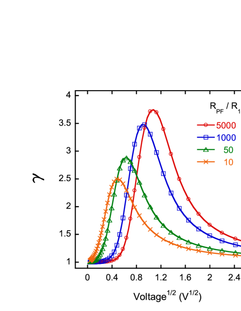
As can be observed in Fig. 7, the ohmic region at low voltages increases when increasing the ratio . This fact is associated with the weight in the conduction process of each element, so that the ohmic region delays the PF contribution when . With regard to the peak of , it is developed in the region of influence of the PF element and may reach values 2. In this way, if an increasing is observed when analyzing the plots of experimental data, the existence of an SCLC mechanism (Child’s law) as the main NL element can be ruled out.
When , becomes short circuited by the PF element when increasing the voltage and the overall behavior becomes asymptotically ohmic by the main contributions to the IV characteristics imposed by .
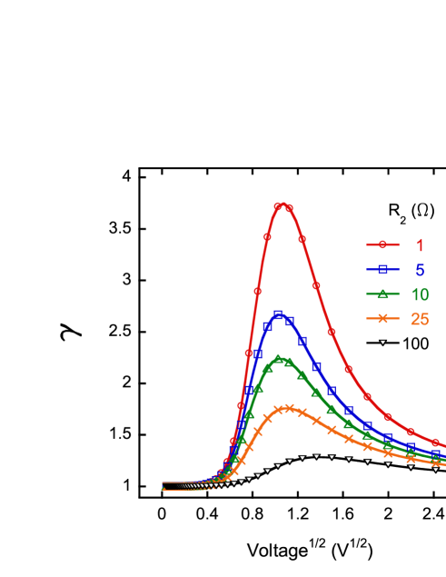
When increasing , the voltage region of the PF element influence is decreased in a way that the peak is reduced (eventually with values 2) and becomes wider, making it barely visible, as depicted in Fig. 8
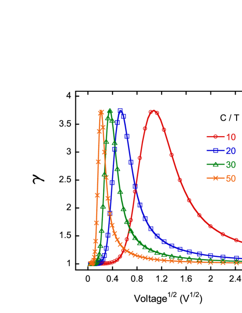
Finally, as shown in Fig. 9, when the ratio increases, the voltage width of the peak, that indicates the extension of the PF influence in the circuit behavior, is reduced. This figure points out the importance of performing IV measurements at different temperatures (see ref.Acha16 ), as this can be a way to determine (or to check) the temperature dependence of microscopic parameters, like (T) (from ) or (from the temperature dependence of ), as well as of other parameters, such as or , which can also be temperature dependent.
It is interesting to note that when performing the fits to the experimental data, the number of fitting parameters can be reduced if the low voltage resistance of the device is measured (usually called ). For example, in the case of the PF element with the ohmic resistances and , by analyzing Eq. 4 in the low voltage limit, it can be shown that .
These examples show the utility of the representation when dealing with the experimental curves measured at different temperatures: just by graphically analyzing the shape of this curve, the existence of a particular NL element can be determined as well as the necessity to include additional ohmic elements as and . Then, the proper IV relation can be used in order to fit the data and to extract the microscopic parameters that govern the conduction mechanism of a device.
III Conclusion
We have shown that the power exponent parameter plotted as a function of can be a useful tool to graphically determine the conduction mechanisms through an interface. This method becomes particularly interesting when the contribution to the conduction process comes from a combination of different elements, including a NL element in series and/or in parallel with ohmic ones. As this is the typical scenario found for some memristive interfaces, the idea is to ease the determination of these elements in order to obtain relevant microscopic information by fitting their IV characteristics with the corresponding expression.
IV Acknowledgment
We would like to thank the financial support by CONICET Grant PIP 112-200801-00930, PICT 2013-0788 and UBACyT 20020130100036BA (2014-2017). We are grateful to A. Schulman, M. Boudard, K. Daoudi and T. Tsuchiya for providing the experimental data shown in Fig.2. We also acknowledge Dr. V. Bekeris for a critical reading of the manuscript, and D. Giménez, E. Pérez Wodtke and D. Rodríguez Melgarejo for their technical assistance.
References
- [1] S. M. Sze and K. K. Ng. Physics of Semiconductor Devices. John Wiley & Sons, 2006.
- [2] F-Ch Chiu. Advances in Materials Science and Engineering, 2014:578168, 2014.
- [3] R. Waser and M. Aono. Nature Materials, 6:833, 2007.
- [4] D. B. Strukov, G. S. Snider, D. R. Stewart, and R. S. Williams. Nature, 453:80, 2008.
- [5] A. Sawa. Materials Today, 11:28, 2008.
- [6] D. S. Shang, Q. Wang, L. D. Chen, R. Dong, X. M. Li, and W. Q. Zhang. Phys. Rev. B, 73:245427, 2006.
- [7] A. Schulman, L. F. Lanosa, and C. Acha. Journal of Applied Physics, 118:044511, 2015.
- [8] A. Bozhko, M. Shupegin, and T. Takagi. Diamond and Related Materials, 11:1753, 2002.
- [9] V. Mikhelashvili, G. Eisenstein, V. Garber, S. Fainleib, G. Bahir, D. Ritter, M. Orenstein, and A. Peer. Journal of Applied Physics, 85:6873, 1999.
- [10] C. Acha. J.Phys.D: Appl.Phys., 44:345301, 2011.
- [11] F. Gomez-Marlasca, N. Ghenzi, A. G. Leyva, C. Albornoz, D. Rubi, P. Stoliar, and P. Levy. Journal of Applied Physics, 113(14):144510, 2013.
- [12] C. Acha, A. Schulman, M. Boudard, K. Daoudi, and T. Tsuchiya. Applied Physics Letters, 109:011603, 2016.
- [13] P. Lunkenheimer, V. Bobnar, A. V. Pronin, A. I. Ritus, A. A. Volkov, and A. Loidl. Phys. Rev. B, 66:052105, 2002.
- [14] J. Blasco, N. Ghenzi, J. Suae, P. Levy, and E. Miranda. IEEE Electron Device Letters, 35:390–392, 2014.
- [15] J. Blasco, N. Ghenzi, J. Suñé, P. Levy, and E. Miranda. Microelectronics Reliability, 55:1–14, 2015.
- [16] A.G. Radwan and M.E. Fouda. On the Mathematical Modeling of Memristor, Memcapacitor, and Meminductor. Springer, 2016.
- [17] I. Vourkas and G. Sirakoulis. Memristor-Based Nanoelectronic Computing Circuits and Architectures. Springer, 2016.
- [18] P. Mark and W. Helfrich. J. Appl. Phys., 33:205, 1962.