Gate voltage control of the interface electrical properties
Abstract
Electron-beam deposition of an insulating granular aluminium or of an off-stoichiometric amorphous alumina layer on a surface is a simple way to get a metallic interface from insulating materials. No heating nor specific preparation of the surface are needed. In this paper, we investigate how the electrical properties of this interface can be tuned by the use of a back gate voltage (electrical field through the substrate). We demonstrate that the slow field-effect observed at room temperature can be used to tune reversibly and in a controlled way the low temperature electrical properties of the interface. In particular, important parameters of a transistor such as the amplitude of the resistance response to gate voltage changes or the existence of an “on” or an “off” state at zero gate voltage and at low temperature can be adjusted in a single sample. This method should be applicable to any -based interface in which oxygen vacancies are involved and might provide a powerful way to study the metal or superconductor insulator transition observed in such systems.
pacs:
72.20.-i 71.30.+h1 Introduction
Various techniques have been successfully used through the last 50 years to put insulating (STO) crystals into a metallic state. With standard chemical doping and high temperature annealing under vacuum [1, 2], the metallic state extends over the bulk of the crystal. With ion-milling [3, 4, 5, 6, 7], UV exposure [8, 9], UHV cleaving [10] and oxide layer deposition [11, 12, 13, 14, 15, 16], the metallic state can be confined close to the STO surface 111Note that if the thickness of the metallic layer can be of less than 10nm for oxide heterostructures, it is much larger (about 100nm or even more) for ion-milled surfaces.. The oxide layer deposition technique was first restricted to the epitaxial growth of oxides by pulsed laser deposition at high temperature, the most famous example being the (LAO/STO) heterostructure [17, 13, 18, 12]. But surface metallic states were also recently observed by using pulsed laser [19, 20, 21, 22] and e-beam [23] depositions of amorphous oxides at room temperature. The respective roles of oxides non stoichiometry (oxygen, cations), adsorbates, ions inter-diffusion and electronic reconstruction in the formation of this surface metallic state remain an active and controversial issue [17, 24, 25, 26, 27, 13, 28, 29, 11, 20, 30, 31, 32, 33, 34].
In this article, we report on electrical field effect measurements of STO crystals, on which an insulating granular aluminum or an oxygen deficient alumina layer (thereafter referred to as the AlOx layer) was deposited at room temperature by electron gun evaporation. We have demonstrated recently that such deposition can put the STO surface into a metallic state [23]. The simplicity of the manufacturing process (no heating, no surface preparation) makes this method very attractive compared to the more sophisticated techniques currently used. The most likely origin of this metallic state is the formation of oxygen vacancies in the STO substrate close to the AlOx/STO interface, the oxygen being “pumped off” from STO when the AlOx layer is deposited on top [23]. Oxygen vacancies in STO are known to release electrons for the conduction and can lead to a metallic state if their concentration is large enough. The exact thickness of this metallic state is not known but its electrical parameters (charge carrier surface density and mobility, sheet resistance value and temperature dependence, etc.) are very similar to the 2D electron gas obtained by the pulsed laser deposition of oxides, which strongly suggests that it is confined close to the interface [23].
When STO crystals are doped in the bulk by chemical impurities or oxygen vacancies, the metal-insulator transition occurs at small charge carrier densities compared to other oxides or even standard doped semi-conductors. The 3D critical charge density which corresponds to the metal-insulator transition is not precisely known but metallic states are reported for impurity densities as low as [2]. The high value of the STO dielectric constant, especially at low temperature, may explain this striking property. At 2D, a metallic-like behaviour is observed for surface charge densities as low as a few [35]. Such a value corresponds to the surface charge density that can be added or removed in a standard field effect experiment, where a gate voltage is applied between the STO surface and a metallic gate over an insulating material (the gate insulator). STO is thus a system in which large modulations of the electrical resistance are expected upon the application of a gate voltage [36].
A large number of electrical field effect experiments have been performed on STO crystal based devices. Many different situations were explored: the STO surface was in the “on” (metallic or superconducting) state or in the “off” (insulating) state when no gate voltage was applied, the bulk of the STO crystal was used as the gate insulator (“back gate” geometry) or another insulating material was deposited on top (“top gate” geometry), the temperature of the measurement was 300K or much lower (4K), etc. The observed resistance response to gate voltage changes are also quite various: they can be fast or slow, small or with relative changes of many orders of magnitude, associated with memory effects and hysteresis, etc. [37, 38, 39, 40, 41, 42, 43, 35, 44, 45, 46, 47, 48, 49, 13, 5, 50, 51, 52, 53, 54, 55, 56, 57, 58, 59, 60, 61]. But in all these studies, the electrical properties of the interface are determined by the fabrication parameters. What we show in this article is that the low temperature electrical properties of our AlOx/STO interface can also be changed after its making.
We studied the field effect in AlOx/STO interfaces in the “back gate” geometry from room T to 4K. Our main results can be summarized as follows. At room temperature, the response to the application of a non-zero gate voltage () is dominated by slow changes of the resistance, which can increase by three orders of magnitude the resistance of a metallic-like interface. Since this slow resistance response is reversible and practically frozen below , it can be used to tune the electronic state (metallic or insulating) of a given starting metallic-like interface, and to stabilize a large range of low temperature properties. For example, a state showing a huge field effect at 4K could be obtained (resistance changing by 6 orders of magnitude with a gate field of 0.6kV/cm). The respective roles of oxygen vacancies electro-migration and standard charge injection processes will be discussed.
2 Elaboration and measurement techniques
The samples were made according to Ref. [23]. STO crystals one side polished, (100) oriented and thick were purchased from Neyco company. The polished surface was simply cleaned by successive ultrasonic bath in trichloroethylene, acetone and alcohol before being mounted in an electron beam evaporator. Al contacts, thick, were deposited first. Then, of insulating granular Al or of deficient alumina passivated by of stoichiometric alumina was deposited between the Al contacts without breaking the vacuum. The deficient alumina layer was obtained by the evaporation of alumina at under an pressure of less than , the stoichiometric alumina layer by the evaporation of alumina at under an pressure of and the insulating granular Al layer by the evaporation of pure Al at under an pressure of . The base pressure of the evaporator is less than . As long as the sheet resistances of the samples are the same, we did not observe any significant difference between the field effect response of granular Al and deficient alumina / STO interfaces.
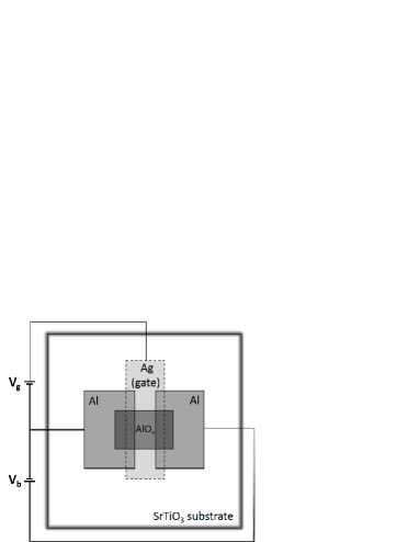
The active channel between the Al contacts (i.e. the part of the surface covered by the AlOx overlayer) has a typical size of . Its electrical resistance was measured in a two contact MOSFET-like configuration 222For metallic samples, two and four contacts configurations could be used and no significant difference was observed. and unless otherwise specified, in the ohmic regime (linear part of the curves, being the bias voltage). Depending on the resistance value, either current bias or voltage bias were used. In our electrical field effect measurements, the gate insulator is the STO substrate itself and no leakage currents were detected with the values used (leakage currents below , maximum absolute value of corresponding to an electric field of ). The bias voltage was usually kept much smaller than in order to avoid any mix up between the two parameters. The gate contact was made on the unpolished side of STO crystal with silver paint and its polarity is such that it is connected to the plus terminal of the source (see Figure 1).
3 Room temperature modulation of the resistance
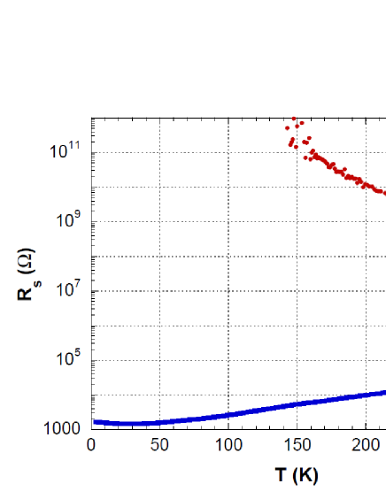
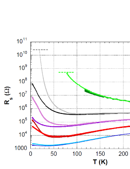
Depending on the oxygen pressure (Al/O ratio during the evaporation), we can get samples with room temperature values from to unmeasurably large values [23]. Typical curves of low and high- samples are plotted on Figure 2 in the range . The resistance of a sample decreases by a factor of 10 between and , with a small resistance increase at lower temperature as observed elsewhere for samples with similar values [48, 27]. The resistance of a sample displays instead a fast increase (close to an exponential) when the temperature is lowered and is already not measurable (R above ) around . The transition from a room temperature metallic-like (temperature coefficient positive around 333Such samples are not metallic in the strict sense since most of them display a clear diverging resistance at low temperature.) to a room temperature insulating-like ( negative around ) behaviour occurs around . We will focus thereafter on metallic-like interfaces, having values in the range at 300K. A resistance increase of which saturates within about 2 hours is observed when the samples are transferred from ambient daylight to darkness, and all the following measurements were thus performed after at least one day in the dark.
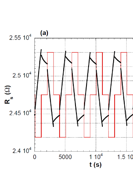
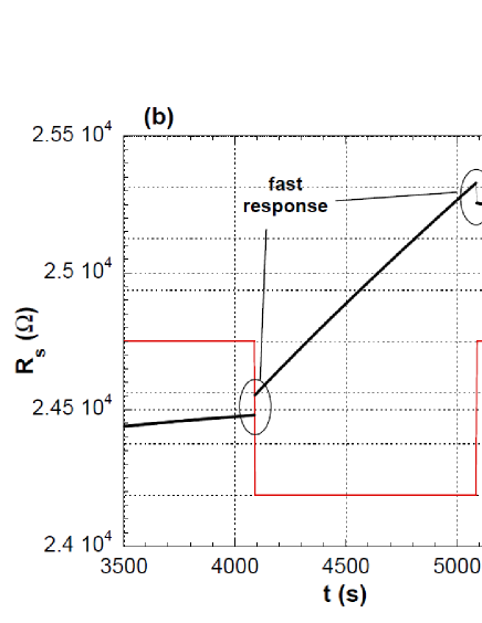
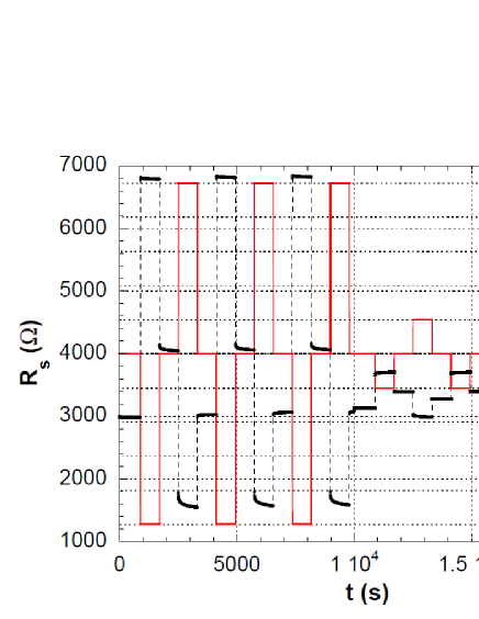
Typical behaviours of such low samples submitted to repeated gate voltage cycles () are plotted in Figure 3. Such cycles are commonly used in STO-based field effect measurements in order to quantify fast and slow responses to changes and to reveal a potential memory of the values experienced by the sample. Apart from small fast (faster than ) changes occurring when is switched, the response is found to be dominated by slow variations. Each stay long under a positive results in a slow resistance decrease with the opposite trend under a negative . Moreover, during the stay, the resistance keeps a memory of the latest experienced by the sample: when is switched back to , the resistance tends to come back to its value before the latest change. But these drifts are much slower than under positive or negative and the restoration is only partial. The values observed over one cycle are therefore not symmetrical to the initial value. modulations are reproducible over many gate voltage cycles and typical values of slow and fast resistance variations are indicated in the legend of Figure 3. Interestingly enough, the resistance modulations are strongly reduced when the samples are exposed to daylight (see Supplementary materials A).
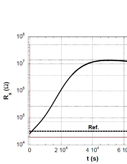
Much larger changes are obtained when non-zero are applied over longer times. Starting from a “fresh” (no history) low- sample (), reaches a minimum value about smaller after few hours under , while a steady increase is observed over under , up to a maximum value of (see Figure 4). Such a value is already beyond the metallic-like to insulating crossover of discussed before.
The fast field-effect can be simply understood as a standard induced charge injection or removal in the system. The fact that a increase is associated with a resistance drop, and a decrease with a resistance jump is in qualitative agreement with the negative sign of the charge carriers obtained by Hall effect measurements [23]. We can go one step further and use the amplitude of the resistance jumps or drops to estimate the surface charge carrier density at the interface. If all the charge carriers involved in the conduction have the same mobility 444The charge carrier mobilities were found to be the in the range for surface and bulk metallic-like states [27, 2]. This approximation should thus be reasonable at least for low- samples., the relative amplitudes of resistance jumps or drops should be equal to the relative changes in the surface charge carrier density (as long as the relative changes are smaller than 1). Assuming a simple plane-plane capacitance geometry, where is the dielectric constant of the STO substrate ( at ) and its thickness (). For the sample of Figure 3 (), and thus are equal to . A change of corresponds at to , which gives a estimate of . This value is in quantitative agreement with Hall effect measurements on samples of similar [23].
Let’s now discuss the prominent slow part of the field effect. In our samples, the charge carriers are supposed to be electrons released by oxygen vacancies in the STO substrate. When , an electrical field exists in the bulk of the STO substrate up to the AlOx/STO interface conducting state. Note that this external field adds to a possible internal field present at the interface when . According to different experiments, oxygen vacancies have a significant mobility in STO at room temperature [7, 62, 54]. It is thus tempting to explain the slow changes observed under non-zero as slow drifts of the oxygen vacancies under this electric field. If (resp. ), the electrical field is such that it pulls (resp. pushes) the positively charged oxygen vacancies further from (resp. closer to) the interface. The concentration of oxygen vacancies close to the AlOx/STO interface thus decreases (resp. increases) under negative (resp. positive) . By analogy with what occurs in disordered induced metal-insulator transition, the decrease of the charge carrier concentration is accompanied by a strong suppression of their mobility below some critical concentration [63]. The crucial role of mobility changes is supported by a quantitative analysis on the sample of figure 4: its surface charge carrier density (deduced from fast resistance jumps and drops, see before) is divided by only 7 between the minimum and maximum states while is multiplied by 400 555The fact that the resistance goes through a maximum under negative in low- samples cannot be understood within this simplified picture. It might result from the combined effects of an internal electrical field at the AlOx/STO interface and of a charge mobility dependence with the distance to the interface.. When is switched back to , the induced electro-migration stops and the resistance shifts are strongly reduced, giving rise to the memory effect described before.
Slow resistance drifts and memory effects are indeed quite common at room temperature in STO-based field effect devices [13, 35, 54]. They are usually attributed to the electro-migration of oxygen vacancies in the STO substrate, an hypothesis which is strengthened by the fact that these features are smaller or absent when top gated insulators are used [55, 35, 56, 53]. But our explanation based on a strong concentration dependence of the charge carriers mobility doesn’t seem to be universal: in amorphous LAO/STO heterostructures, the large and slow changes are accompanied by large changes of the surface charge density, with only a negligible alteration of the mobility [54].
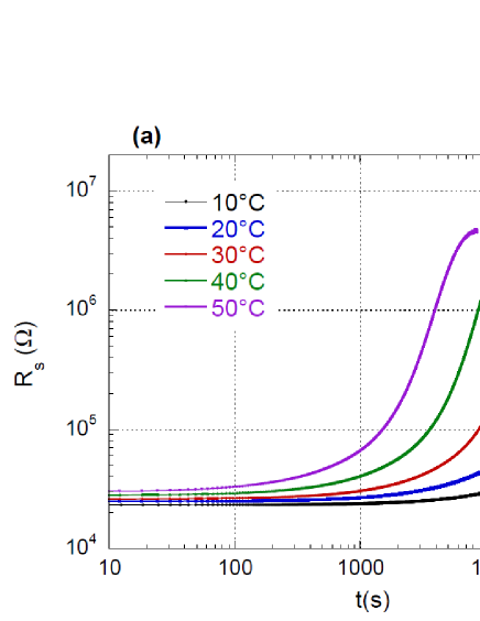
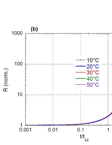
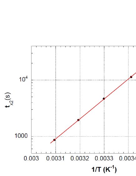
In order to test in more detail the oxygen vacancy electro-migration hypothesis, we have studied how the slow drifts were affected by temperature changes around . Our protocol was the following. The sample was first let to equilibrate under until reached its minimum value. Then, was changed to and the subsequent increase was measured as a function of time. The same protocol was repeated at different temperatures between and . Typical results are plotted in Figure 5. It is clearly seen that the changes are strongly slowed down when T is reduced. Moreover, all the curves can be merged together far from the saturation regime by normalizing to its value at and the time scale by an ad-hoc characteristic time for each T (see the legend of Figure 6 for the exact definition of this characteristic time). Even if the T range is small in kelvin scale, the T dependence of the characteristic times is close to an activated behavior (see Figure 6), with an activation energy of 666The exact definition of the characteristic times will change the time scale in Figure 6 but not the activation energy extracted.. A similar value was found in a much more resistive sample, having . This value of is in agreement with previous experimental and theoretical estimates for oxygen vacancy diffusion coefficient in STO [64, 62, 65], which strengthens our hypothesis that the electro-migration of oxygen vacancies (isolated or as clusters) is responsible of the slow resistance drifts observed under . In amorphous LAO/STO interfaces [54], no quantitative estimate of the activation energy was done, but the resistance drifts are absent below , in qualitative agreement with the strong temperature dependence highlighted in Figures 5 and 6.
4 tuned interfaces measured at low temperature
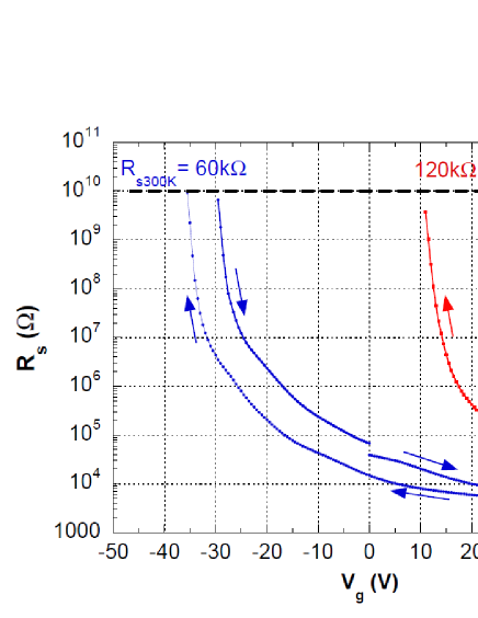
We are now going to demonstrate how this strong temperature dependence of the slow field effect can be used to tune the low temperature properties of a unique AlOx/STO interface. The protocol is as follows. Starting with a metallic-like sample having , we first apply a negative of until the desired value is obtained (values up to can be achieved, see before). Then, we quickly cool down the sample below , usually under , in order to freeze the sample parameters. At this temperature, the characteristic time of the slow resistance drifts are already so long that they cannot be measured in practice. Typical curves of such -tuned sample are plotted in Figure 7. It is seen that, like in non -tuned samples, the behavior can indeed be changed from metallic-like ( around 300K) to insulating-like ( around 300K) when at exceeds . A large range from a few to non measurable resistances () can be obtained at 4K. The low T differences observed between cool-down and warm-up curves are due to the irreversible resistance increase which occurs during the first cycles at low T (see Supplementary materials B).
The typical response of a non -tuned sample () to repeated cycles (0V, , 0V, ) is plotted on Figure 8. The fast field effect now dominates the modulation and is much larger than at for the same sample: is multiplied by more than 2 after a change from to , compared to an increase of less than 1% at . A memory effect is also present, i.e. the value at = 0V depends of the previous applied.
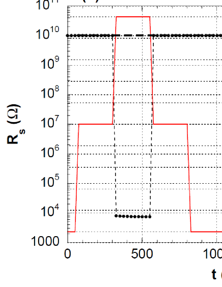
But when tuned samples having larger values are measured, the electrical field effects change dramatically. The relative difference is about 50% between and at when (non tuned sample) and it becomes as large as 6 orders of magnitude when following tuning (see Figure 9). When is further increased, the resistance of the interface becomes unmeasurable under (transistor in the “off” state, ) and is as low as under . Moreover and like in non tuned samples, the large modulations observed at are accompanied by memory effects at , which take the form of an hysteresis in the curves of Figure 10. Note that when increases, the values become also strongly bias dependent.
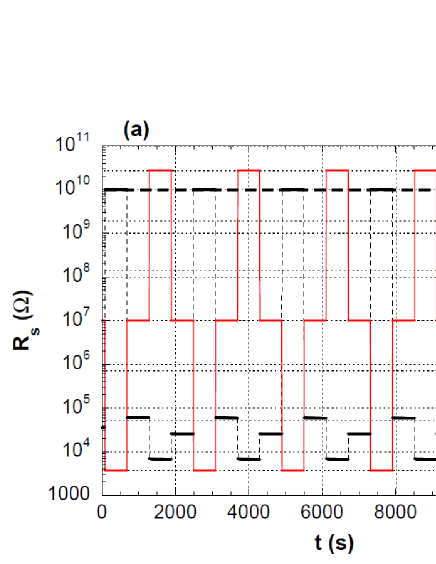
Like at room temperature, the amplitude of the instantaneous field effect in non tuned low- samples is compatible with a standard charge injection process by the gate. According to our Hall effect measurements on a low- sample, we know that the surface charge density is almost constant with the temperature between and 777For a sample having at , was found to increase from at up to at , before decreasing down to at .. But the dielectric constant of STO has a strong temperature dependence: is around 300 at , 2000 at , 20000 at (under a small electric field) [66, 67] and 10000 for (electrical field of ) [66]. We thus expect the surface charge densities induced by the gate voltage to be about ten times larger at and 100 times larger at than at (at small enough ). It corresponds roughly to what is indeed measured for the low- sample of Figure 8 when is small: at 300K, at 77K and at 4K. The fact that the modulation becomes larger in relative value in samples having increasing values can simply be explained by a decrease of their surface charge densities.
As for tuned high- samples, large resistance modulations at low temperatures have been reported in many studies on STO-based field effect devices in the back gate configuration [5, 48, 46]. Beyond the effect of a change, the mobility was also found to play a major role in the resistance modulations [5, 48, 60]. Under , the electron gas is compressed closer to the interface and the mobility is lowered, while under , the electron gas is extended towards the STO volume and the mobility is enhanced. The complete understanding of gating effects also requires the inclusion of the permittivity nonlinearities with the electric field [48].
The origin of the memory effect and the hysteresis observed in Figures 8 and 9 remains unclear. Dielectric studies have shown that a ferroelectric state can be induced by a strong enough electrical field in STO crystals, due to the proximity of the ferroelectric transition [67]. This ferroelectric state was usually found to be suppressed when T is increased beyond . Hysteresis and remnant polarization were measured at in Ref. [68, 69], but also under smaller fields in LAO/STO interfaces [46, 48, 70]. In Ref. [70], the resistance hysteresis was found to be related to a field induced polar order localized in the STO substrate about below the LAO/STO interface [70]. Interestingly enough, small or no hysteresis was found at low T in field effect measurements in top-gate configuration [55], indicating that the STO substrate plays the dominant role in the effect. In our case, a memory effect is visible at already at but not at up to .
5 Conclusion
Our results show how the electrical properties of a metallic-like AlOx/STO interface can be tuned by the use of a back-gate voltage . At room temperature, a slow increase of the resistance is observed under a negative . This resistance increase can be large (many orders of magnitude) if is applied for a long enough time and the initial resistance value can be restored with the use of a positive . The sample sheet resistance can thus be tuned on a controlled and reversible way to any value spanning from a metallic-like (, at ) to an insulating-like behavior (, at ). The activation energy of these slow resistance change time scales is about which strongly suggests that they are related to oxygen vacancy electro-migration. By pulling the oxygen vacancies in the volume of the STO crystal (the gate insulator material), the electrical field reduces the charge carriers density and mobility.
If the interface resistance is tuned at room temperature and then rapidly cooled down below , a large set of stable interface electrical properties can be obtained. Such process can be used for example to increase the field effect amplitude at : fast resistance changes as large as six orders of magnitude can thus be obtained under cycles. We believe that this tuning technique at room temperature should also be applicable to the other 2D STO-based metallic systems where similar slow field effects have been reported. Beyond the adjustment of low temperature transistors parameters, it should allow the fine study of the metal-insulator transition or even the transition to the superconducting state as a function of the interface parameters (charge carriers density and mobility) in a single sample.
References
- [1] Frederikse H P, Thurber W R and Hosler W R 1964 Physical Review 134 442
- [2] Spinelli A, Torija M A, Liu C, Jan C and Leighton C 2010 Physical Review B 81 155110
- [3] Reagor D W and Butko V Y 2005 Nature Materials 4 593
- [4] Kan D, Terashima T, Kanda R, Masuno A, Tanaka K, Chu S, Kan H, Ishizumi A, Kanemitsu Y, Shimakawa Y et al. 2005 Nature Materials 4 816
- [5] Ngai J, Segal Y, Su D, Zhu Y, Walker F, Ismail-Beigi S, Le Hur K and Ahn C 2010 Physical Review B 81 241307
- [6] Herranz G, Copie O, Gentils A, Tafra E, Basletić M, Fortuna F, Bouzehouane K, Fusil S, Jacquet É, Carrétéro C et al. 2010 Journal of Applied Physics 107 103704
- [7] Gross H, Bansal N, Kim Y S and Oh S 2011 Journal of Applied Physics 110 073704
- [8] Kozuka Y, Hikita Y, Susaki T and Hwang H 2007 Physical Review B 76 085129
- [9] Meevasana W, King P, He R, Mo S, Hashimoto M, Tamai A, Songsiriritthigul P, Baumberger F and Shen Z 2011 Nature Materials 10 114
- [10] Santander-Syro A, Copie O, Kondo T, Fortuna F, Pailhes S, Weht R, Qiu X, Bertran F, Nicolaou A, Taleb-Ibrahimi A et al. 2011 Nature 469 189
- [11] Chen Y, Bovet N, Trier F, Christensen D, Qu F, Andersen N H, Kasama T, Zhang W, Giraud R, Dufouleur J et al. 2013 Nature Communications 4 1371
- [12] Carretero C 2010 Hétérostructures d’oxydes de structure pérovskite : propriétés structurales et électroniques de l’interface LaAlO3/SrTiO3 Ph.D. thesis Université Pierre et Marie Curie
- [13] Thiel S 2009 Study of Interface Properties in LaAlO3/SrTiO3 Heterostructures Ph.D. thesis Universität Augsburg
- [14] Basletic M, Maurice J L, Carrétéro C, Herranz G, Copie O, Bibes M, Jacquet É, Bouzehouane K, Fusil S and Barthélémy A 2008 Nature Materials 7 621
- [15] Sing M, Berner G, Goß K, Müller A, Ruff A, Wetscherek A, Thiel S, Mannhart J, Pauli S, Schneider C et al. 2009 Physical Review Letters 102 176805
- [16] Reyren N, Thiel S, Caviglia A, Kourkoutis L F, Hammerl G, Richter C, Schneider C, Kopp T, Rüetschi A S, Jaccard D et al. 2007 Science 317 1196
- [17] Ohtomo A and Hwang H 2004 Nature 427 423
- [18] Huijben 2006 Interface Engineering for Oxide Electronics: Tuning electronic properties by atomically controlled growth Ph.D. thesis University of Twente
- [19] Chen Y, Pryds N, Kleibeuker J E, Koster G, Sun J, Stamate E, Shen B, Rijnders G and Linderoth S 2011 Nano Letters 11 3774
- [20] Liu Z, Li C, Lü W, Huang X, Huang Z, Zeng S, Qiu X, Huang L, Annadi A, Chen J et al. 2013 Physical Review X 3 021010
- [21] Fuchs D, Schäfer R, Sleem A, Schneider R, Thelen R and von Löhneysen H 2014 Applied Physics Letters 105 092602
- [22] Scigaj M, Gázquez J, Varela M, Fontcuberta J, Herranz G and Sanchez F 2015 Solid State Ionics 281 68
- [23] Delahaye J and Grenet T 2012 Journal of Physics D: Applied Physics 45 315301
- [24] Nakagawa N, Hwang H Y and Muller D A 2006 Nature Materials 5 204
- [25] Kalabukhov A, Gunnarsson R, Börjesson J, Olsson E, Claeson T and Winkler D 2007 Physical Review B 75 121404
- [26] Siemons W, Koster G, Yamamoto H, Harrison W A, Lucovsky G, Geballe T H, Blank D H and Beasley M R 2007 Physical Review Letters 98 196802
- [27] Herranz G, Basletić M, Bibes M, Carrétéro C, Tafra E, Jacquet E, Bouzehouane K, Deranlot C, Hamzić A, Broto J M et al. 2007 Physical Review Letters 98 216803
- [28] Cancellieri C, Reyren N, Gariglio S, Caviglia A, Triscone J M et al. 2010 Europhysics Letters 91 17004
- [29] Herranz G, Sánchez F, Dix N, Scigaj M and Fontcuberta J 2012 Scientific Reports 2 758
- [30] Breckenfeld E, Bronn N, Karthik J, Damodaran A, Lee S, Mason N and Martin L 2013 Physical Review Letters 110 196804
- [31] Asmara T, Annadi A, Santoso I, Gogoi P, Kotlov A, Omer H, Motapothula M, Breese M, Rübhausen M, Venkatesan T et al. 2014 Nature Communications 5 3663
- [32] Li C, Liu Z, Lü W, Wang X R, Annadi A, Huang Z, Zeng S, Venkatesan T et al. 2015 Scientific Reports 5 13314
- [33] Gariglio S, Fête A and Triscone J M 2015 Journal of Physics: Condensed Matter 27 283201
- [34] Scheiderer P, Pfaff F, Gabel J, Kamp M, Sing M and Claessen R 2015 Physical Review B 92 195422
- [35] Thiel S, Hammerl G, Schmehl A, Schneider C and Mannhart J 2006 Science 313 1942
- [36] Ahn C, Bhattacharya A, Di Ventra M, Eckstein J, Frisbie C D, Gershenson M, Goldman A, Inoue I, Mannhart J, Millis A J et al. 2006 Reviews of Modern Physics 78 1185
- [37] Yoshida C, Tamura H, Yoshida A, Kataoka Y, Fujimaki N and Yokoyama N 1996 Japanese Journal of Applied Physics 35 5691
- [38] Pallecchi I, Grassano G, Marr D, Pellegrino L, Putti M and Siri A S 2001 Applied Physics Letters 78 2244
- [39] Ueno K, Inoue I, Akoh H, Kawasaki M, Tokura Y and Takagi H 2003 Applied Physics Letters 83 1755
- [40] Inoue I 2004 Electrostatic tuning of oxide interfaces annual Report FY2003, Correlated Electron Research Center (CERC)
- [41] Shibuya K, Ohnishi T, Lippmaa M, Kawasaki M and Koinuma H 2004 Applied Physics Letters 85 425
- [42] Shibuya K, Ohnishi T, Uozumi T, Sato T, Lippmaa M, Kawasaki M, Nakajima K, Chikyow T and Koinuma H 2006 Applied Physics Letters 88 212116
- [43] Nakamura H, Takagi H, Inoue I H, Takahashi Y, Hasegawa T and Tokura Y 2006 Applied Physics Letters 89 133504
- [44] Shibuya K, Ohnishi T, Sato T and Lippmaa M 2007 Journal of Applied Physics 102 083713
- [45] Shibuya K, Ohnishi T, Uozumi T, Sato T, Nishio K and Lippmaa M 2008 Applied Physics Letters 92 032109
- [46] Caviglia A, Gariglio S, Reyren N, Jaccard D, Schneider T, Gabay M, Thiel S, Hammerl G, Mannhart J and Triscone J M 2008 Nature 456 624
- [47] Ueno K, Nakamura S, Shimotani H, Ohtomo A, Kimura N, Nojima T, Aoki H, Iwasa Y and Kawasaki M 2008 Nature Materials 7 855
- [48] Bell C, Harashima S, Kozuka Y, Kim M, Kim B, Hikita Y and Hwang H 2009 Physical Review Letters 103 226802
- [49] Cen C, Thiel S, Mannhart J and Levy J 2009 Science 323 1026
- [50] Nishio K, Abe T, Takahashi R and Lippmaa M 2010 Japanese Journal of Applied Physics 49 125701
- [51] Lee Y, Clement C, Hellerstedt J, Kinney J, Kinnischtzke L, Leng X, Snyder S D and Goldman A M 2011 Phys. Rev. Lett. 106(13) 136809 URL http://link.aps.org/doi/10.1103/PhysRevLett.106.136809
- [52] Li M, Graf T, Schladt T D, Jiang X and Parkin S S P 2012 Phys. Rev. Lett. 109(19) 196803 URL http://link.aps.org/doi/10.1103/PhysRevLett.109.196803
- [53] Förg B, Richter C and Mannhart J 2012 Applied Physics Letters 100 053506
- [54] Christensen D, Trier F, Chen Y, Smith A, Nygård J and Pryds N 2013 Applied Physics Letters 102 021602
- [55] Hosoda M, Bell C, Hikita Y and Hwang H Y 2013 Applied Physics Letters 102 103507
- [56] Eyvazov A B, Inoue I H, Stoliar P, Rozenberg M J and Panagopoulos C 2013 Scientific Reports 3 1038
- [57] Eerkes P D, van der Wiel W G and Hilgenkamp H 2013 Applied Physics Letters 103 201603
- [58] Biscaras J, Hurand S, Feuillet-Palma C, Rastogi A, Budhani R, Reyren N, Lesne E, Lesueur J and Bergeal N 2014 Scientific Reports 4 6788
- [59] Gallagher P, Lee M, Williams J R and Goldhaber-Gordon D 2014 Nature Physics 10 748
- [60] Liu W, Gariglio S, Fête A, Li D, Boselli M, Stornaiuolo D and Triscone J M 2015 Applied Physics Letters Materials 3 062805
- [61] Hurand S, Jouan A, Feuillet-Palma C, Singh G, Biscaras J, Lesne E, Reyren N, Barthélémy A, Bibes M, Villegas J E, Ulysse C, Lafosse X, Pannetier-Lecoeur M, Caprara S, Grilli M, Lesueur J and Bergeal N 2015 Scientific Reports 5 12751
- [62] Schultz M and Klein L 2007 Applied Physics Letters 91 151104
- [63] Gross H 2009 In-situ study of emerging metallicity and memory effect on ion beam bombarded strontium titane surface Ph.D. thesis The State University of New Jersey
- [64] Cordero F 2007 Physical Review B 76 172106
- [65] Cuong D D, Lee B, Choi K M, Ahn H S, Han S and Lee J 2007 Physical Review Letters 98(11) 115503
- [66] Neville R C, Hoeneisen B and Mead C A 1972 Journal of Applied Physics 43 2124
- [67] Müller K A and Burkard H 1979 Physical Review B 19 3593
- [68] Hemberger J, Nicklas M, Viana R, Lunkenheimer P, Loidl A and Böhmer R 1996 Journal of Physics Condensed Matter 8 4673
- [69] Saifi M A and Cross L E 1970 Physical Review B 2 677
- [70] Rössle M, Kim K W, Dubroka A, Marsik P, Wang C N, Jany R, Richter C, Mannhart J, Schneider C W, Frano A, Wochner P, Lu Y, Keimer B, Shukla D K, Strempfer J and Bernhard C 2013 Physical Review Letters 110 136805