Theory of electron-plasmon coupling in semiconductors
Abstract
The ability to manipulate plasmons is driving new developments in electronics, optics, sensing, energy, and medicine. Despite the massive momentum of experimental research in this direction, a predictive quantum-mechanical framework for describing electron-plasmon interactions in real materials is still missing. Here, starting from a many-body Green’s function approach, we develop an ab initio approach for investigating electron-plasmon coupling in solids. As a first demonstration of this methodology, we show that electron-plasmon scattering is the primary mechanism for the cooling of hot carriers in doped silicon, it is key to explain measured electron mobilities at high doping, and it leads to a quantum zero-point renormalization of the band gap in agreement with experiment.
pacs:
Plasmons are collective oscillations of electrons in solids that can exist even in the absence of an external driving field. During the last decade plasmons generated tremendous interest owing to the rise of plasmonics, the science of manipulating light and light-matter interactions using surface plasmon polaritons Lal et al. (2007). Plasmonic materials and devices show exceptional promise in the areas of nanoelectronics Walters et al. (2010), photovoltaics Atwater and Polman (2010); Brongersma et al. (2015), and radiation treatment therapy Lukianova-Hleb et al. (2013); Zhang et al. (2013). While the electrodynamic laws governing plasmonics at macroscopic length-scales are well understood Maier (2007); Pitarke et al. (2007), little is known about the interaction of plasmons with matter at the atomic scale. For example questions pertaining the interaction between plasmons and charge carriers in semiconductors have not been addressed on quantitative grounds, yet they are critical to engineering materials for semiconductor plasmonics Ozbay (2006). Up to now microscopic quantum-mechanical theories of electron-plasmon interactions have been limited to idealised models of solids, such as the homogeneous electron gas Bohm and Pines (1953); Pines and Schrieffer (1962). While these models laid the theoretical foundations of the theory, they are not suitable for predictive calculations.
In this work we introduce a first-principles method to study electron-plasmon coupling in solids. As a first application we focus on doped semiconductors, where the manifestations of electron-plasmon coupling are most spectacular. In contrast to metals and insulators, doped semiconductors can sustain ‘thermal plasmons’, that is plasmons with energies comparable to those of lattice vibrations. Under these conditions electron-plasmon interactions can modify carrier lifetimes, mobilities, and optical gaps in a manner similar to electron-phonon interactions. Using this method we find that, in the case of degenerate -type silicon, thermal plasmons lead to ultrafast relaxation of hot carriers, provide the main bottleneck to carrier mobility, and induce a zero-point renormalization of the band gap that exceeds the phonon-induced renormalization.
In free-electron metals the energy of a plasmon is , where is the Planck constant, is the dielectric permittivity of vacuum, and , , and are the electron charge, mass, and density, respectively. At typical metallic densities, as in common plasmonic metals such as Au and Ag (- cm-3), plasmons have characteristic energies in the range of 5-10 eV. In these cases electron-plasmon scattering is suppressed by the energy-conservation selection rule. At variance with this scenario, in doped semiconductors the electron mass in the above expression is replaced by the band effective mass, and the vacuum permittivity is replaced by the dielectric constant. As a result the plasmon energy is considerably smaller, and at standard doping levels it can easily reach the thermal range, 10-100 meV. Under these conditions electrons can exchange energy with plasmons, hence the populations of carriers and plasmons become mutually coupled.
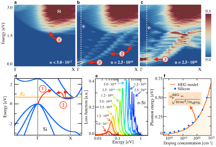
In order to investigate the consequences of this coupling, we start by characterizing plasmonic excitations in doped silicon from first principles. Figure 1 shows the calculated electron energy loss function, , which encodes information about how an electron travelling through a solid dissipates energy Nozières and Pines (1959). Here denotes the head of the inverse dielectric matrix for the wavevector and the frequency , evaluated within the random phase approximation Adler (1962); Wiser (1963). In the case of intrinsic silicon at zero temperature (Fig. 1a) the loss function exhibits a continuous energy distribution (brown region) with a threshold set by the fundamental gap. This broad structure arises from interband transitions from the filled valence bands to the empty conduction bands, and physically corresponds to the generation of electron-hole pairs by impact ionization. This is schematically indicated as ‘process 1’ in Fig. 1d. The scenario changes drastically in the case of doped silicon. Fig. 1b and Fig. 1c show the loss function of heavily -doped silicon, corresponding to cm-3 and cm-3, respectively. As a result of the partial filling of the conduction band valley near the point of the Brillouin zone, new dissipation channels become available. In particular, ‘process 2’ in Fig. 1b corresponds to the generation of low-energy electron-hole pairs. In this case we see sharp structures which define ‘ghost’ bands as a function of the momentum loss . These features are understood in terms of intraband and interband transitions from occupied initial states with wavevector near the bottom of the conduction band to empty final states of wavevector . The intensity of these features increases with the doping level from Fig. 1b to Fig. 1c. The peaks in the loss function denoted by ‘process 3’ cannot be explained in terms of the previous two mechanisms. In fact for these structures are much sharper than those described above, and exist below the energy (momentum) threshold for the generation of electron-hole pairs via interband (intraband) transitions. These processes correspond to the emission of plasmons, and are characterised by well-defined energy resonances, as it is shown by Fig. 1e for . By mapping these plasmon peaks in the loss function we can see in Fig. 1f that the plasmon energy scales with the carrier concentration, following the same trend expected for a homogeneous electron gas. In this figure we also see that the plasmon energy is highly tunable via doping, from thermal energies at carrier densities around 1018 cm-3, to half an electronvolt at densities near 1021 cm-3.
At large momentum transfer the distinction between plasmons and electron-hole pairs is no longer meaningful, since the fluctuations of the charge density happen on length-scales approaching the size of the crystal unit cell. In the following we identify plasmons in the loss function by analogy with the homogeneous electron gas, where well-defined plasma excitations exist only for momenta below the electron-hole continuum Pines (1999). For a plasmon of energy the critical momentum is given by the wavevector , with and being the Fermi wavevector and the Fermi energy, respectively. The critical wavevector marks the onset of Landau damping, that is, the decay of a plasmon upon excitation of an electron-hole pair. Thus, for thermal plasmons are undamped collective phenomena with lifetimes set by plasmon-phonon and plasmon-plasmon scattering processes sup . This boundary is shown as white dashed lines in Fig. 1b and Fig. 1c.
In order to investigate the effects of plasmons on the electronic structure we generalise Pines’ theory of electron-plasmon interactions in the homogeneous electron gas Pines (1999) to ab initio calculations for crystalline solids. Our strategy consists of the following steps: (i) We identify the energy vs. wavevector dispersion relations of thermal plasmons. This is achieved by determining the plasma energies from the poles of Im for momenta below the critical wavevector Nozieres and Pines (1958). (ii) We single out the plasmonic contribution to the macroscopic dielectric function via the Taylor expansion in the vicinity of the plasmon frequency . (iii) We calculate the electron-plasmon self-energy starting from many-body perturbation theory, and retain only the plasmonic screening. This leads to the retarded electron self-energy in Raleigh-Schrödinger perturbation theory Mahan (2000):
| (1) |
In this expression and are Bloch wavevectors, and band indices, and Kohn-Sham eigenvalues, and Bose-Einstein and Fermi-Dirac occupations, respectively, and a positive infinitesimal. The summation runs over all states and the integral is over the Brillouin zone of volume . The quantities represent the electron-plasmon scattering matrix elements between the initial state and the final state , and are given by:
| (2) |
with being the volume of one unit cell. Eqs. (1) and (2) are derived in the Appendix. The present approach to electron-plasmon coupling in semiconductors is formally identical to the standard theory of electron-phonon interactions Engelsberg and Schrieffer (1963). In particular, the divergence of the electron-plasmon matrix elements at long wavelengths is reminiscent of the Fröhlich interaction between electrons and longitudinal-optical phonons in polar semiconductors Fröhlich (1954); Verdi and Giustino (2015). This analogy is consistent with the fact that bulk plasmons are longitudinal waves. We now analyse the consequences of the self-energy in Eq. (1).
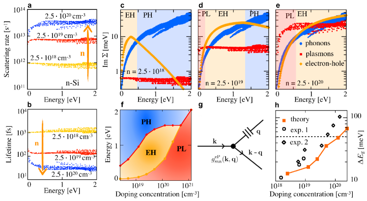
From the imaginary part of the self-energy in Eq. (1) we obtain the rate of electron scattering by thermal plasmons, using . Physically the two denominators in Eq. (1) describe processes of one-plasmon absorption and emission, respectively. A diagrammatic representation of these processes is given in Fig. 2g. Multi-plasmon processes are not included in the present formalism, similarly to the case of electron-phonon interactions Engelsberg and Schrieffer (1963), therefore we limit our discussion to low temperatures (). Fig. 2a shows the calculated electron-plasmon scattering rates in -type silicon. The carrier energies are referred to the conduction band edge. For standard doping levels ( cm-3) the scattering rates fall below s-1 as a result of the low intensity of the plasmon peaks in Fig. 1e, which is reflected in the strength of the matrix elements in Eq. (2). However, at doping levels above 1018 cm-3, the strength of the plasmon peak in the loss function increases considerably, and the frequency of scattering by thermal plasmons becomes comparable to electron-phonon scattering rates, 1012-1014 s-1 Jalabert and Das Sarma (1990); Bernardi et al. (2014). Fig. 2a shows that at even higher doping levels these rates keep increasing by orders of magnitude, and eventually dominate the cooling dynamics of excited carriers.
A complementary perspective on the carrier dynamics is provided by Fig. 2b. Here we show the electron lifetimes corresponding to the rates in Fig. 2a, calculated as . Time-resolved reflectivity measurements of non-degenerate silicon ( cm-3 electrons photo-excited at 0.8 eV above the band edge) indicate thermalisation rates around 350 fs Doany and Grischkowsky (1988). In the same doping range our calculations yield plasmon-limited carrier lifetimes well above 10 ps, indicating that under these conditions electron-plasmon scattering is ineffective. However, the scenario changes drastically for degenerate silicon, for which we calculate lifetimes in the sub-picosecond regime. In particular, for doping levels in the range -1020 cm-3 the electron-plasmon scattering reduces the carrier lifetimes to 25-150 fs. In these conditions electron-phonon and electron-plasmon scattering become competing mechanisms for hot-carrier thermalisation.
In order to quantify the importance of electron-plasmon scattering we compare in Fig. 2c-e the imaginary part of the electron self-energy associated with (i) electron-plasmon interactions, (ii) electron-phonon interactions, and (iii) and electron-hole pair generation. The methods of calculation of (ii) and (iii) are described in the Supplemental Materials sup . From this comparison we deduce that plasmons become increasingly important towards higher doping, and their effect is most pronounced in the vicinity of the band edge. By identifying the largest contribution for each doping level and for each electron energy, we can construct the ‘scattering phase diagram’ shown in Fig.2f. This diagram illustrates the regions in the energy vs. doping space where each scattering mechanism dominates. Unexpectedly in degenerate silicon electron-plasmon scattering represents the dominant mechanism for hot-carrier relaxation. This finding could provide new opportunities in the study of semiconductor-based plasmonics, for example by engineering the doping concentration so as to selectively target the ‘plasmon region’ in Fig.2f.
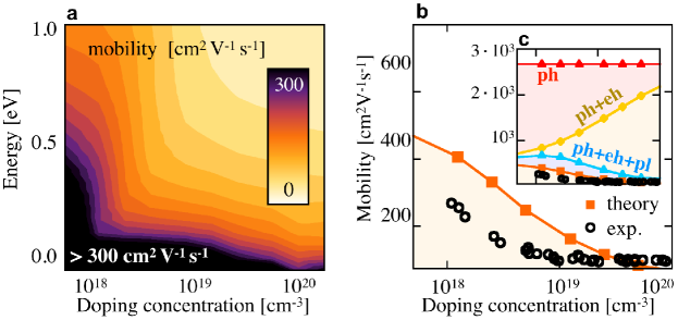
We also evaluated the impact of electron-plasmon scattering processes on the carrier mobility in silicon, by using the lifetimes computed above as a first approximation to the carrier relaxation times. As shown in Fig. S1 sup , the explicit inclusion of electron-phonon scattering is essential to achieve a good agreement with experiment. On the other hand, were we to consider only electron-phonon scattering and electron-hole pair generation, we would overestimate the experimental mobilities by more than an order of magnitude.
The real part of the electron self-energy in Eq. (1) allows us to evaluate the renormalization of the electron energy levels arising from the dressing of electron quasiparticles by virtual plasmons. Since the renormalization of semiconductor band gaps induced by electron-phonon interactions attracted considerable interest lately Marini (2008); Giustino et al. (2010); Cannuccia and Marini (2011); Botti and Marques (2013); Monserrat et al. (2014); Antonius et al. (2014), we here concentrate on the quantum zero-point renormalization of the fundamental gap of silicon. Computational details of the calculations and convergence tests are reported in the Supplemental Material sup . Considering for definiteness a carrier density of cm-3, we find that the electron-plasmon coupling lowers the conduction band edge by meV at zero temperature, and rises the valence band edge by meV. For carrier concentrations of cm-3 and cm-3 we verified that the BGN changes by less that 1 meV for temperatures up to 600 K (see Supplemental Material sup ). As a result at this doping concentration the band gap redshifts by meV. This phenomenology is entirely analogous to the zero-point renormalization from electron-phonon interactions Giustino et al. (2010). Our finding is consistent with the fact that the self-energy in Eq. (1) and the matrix element in Eq. (2) are formally identical to those that one encounters in the study of the Fröhlich interaction. The doping-induced band gap renormalization was also reported in a recent work on monolayer MoS2 Liang and Yang (2015), therefore we expect this feature to hold general validity in doped semiconductors. In order to perform a quantitative comparison with experiment, we show in Fig. 2h our calculated plasmonic band gap renormalization and measurements of the indirect absorption onset in doped silicon Balkanski et al. (1969); Aw et al. (1991). We can see that there is already good agreement between theory and experiment, even if we are considering only electron-plasmon couplings as the sole source of band gap renormalization. Surprisingly the magnitude of the renormalization, 15-70 meV, is comparable to the zero-point shift induced by electron-phonon interactions, 60-72 meV Zacharias et al. (2015).
In summary, we presented an ab initio approach to electron-plasmon coupling in doped semiconductors. We showed that electron-plasmon interactions are strong and ubiquitous in a prototypical semiconductor such as doped silicon, as revealed by their effect on carrier dynamics, transport, and optical properties. This finding calls for a systematic investigation of electron-plasmon couplings in a wide class of materials. More generally, a detailed understanding of the interaction between electrons and thermal plasmons via predictive atomic-scale calculations could provide a key into the design of plasmonic semiconductors, for example by using phase diagrams such as in Fig. 2f to tailor doping levels and excitation energies to selectively target strong-coupling regimes. Finally, the striking similarity between electron-plasmon coupling and the Fröhlich coupling in polar materials may open new avenues to probe plasmon-induced photoemission kinks Damascelli et al. (2003), polaron satellites Moser et al. (2013); Caruso et al. (2015); Caruso and Giustino (2015), as well as superconductivity, in analogy with the case of electron-phonon interactions.Bustarret et al. (2006); Ekimov et al. (2004); Boeri et al. (2004); Lee and Pickett (2004); Blase et al. (2004); Giustino et al. (2007).
Acknowledgements.
F.C. acknowledges discussions with C. Verdi and S. Poncé. The research leading to these results has received funding from the Leverhulme Trust (Grant RL-2012-001), the Graphene Flagship (EU FP7 grant no. 604391), the UK Engineering and Physical Sciences Research Council (Grant No. EP/J009857/1). Supercomputing time was provided by the University of Oxford Advanced Research Computing facility (http://dx.doi.org/10.5281/zenodo.22558) and the ARCHER UK National Supercomputing Service.Appendix A Electron self-energy for the electron-plasmon interaction
Here we provide a derivation of the electron-plasmon coupling strength and the self-energy [Eq. (1) and (2)] by generalizing the theory of electron-plasmon interaction for the homogeneous electron gas to the case of crystalline solids. We start from the electron self-energy in the approximation Hedin (1965); Aulbur et al. (2000); Hybertsen and Louie (1986):
| (3) |
where are the optical matrix elements, is the chemical potential, and . The matrix represents the screened Coulomb interaction, and is obtained from the bare Coulomb interaction via the inverse dielectric matrix . The spectral representation of is given by:
| (4) |
The dielectric matrix may be decomposed into:
| (5) |
where is the inverse macroscopic dielectric function. Since the plasmon energy is defined by the condition , the plasmonic contribution to the dielectric matrix can be singled out by Taylor-expanding around the plasmon energy. Following Pines and Schrieffer Pines and Schrieffer (1962) we have:
| (6) |
Making use of the identity , and combining Eqs. (3), (4), and (6) yields the electron-plasmon self-energy:
| (7) |
This expression may be recast into the form of a self-energy describing the interaction between electrons and bosons in the Migdal approximation Engelsberg and Platzman (1966); Lundqvist (1967); Langreth (1970); Overhauser (1971); Mahan (2000):
| (8) |
Since for doped semiconductors is typically within the first Brillouin zone, we dropped the dependence on the reciprocal lattice vectors . The matrix elements appearing in this expression are defined in Eq. (2); represents the standard non-interacting (Kohn-Sham) electron Green’s function, , and we introduced the ‘plasmon propagator’: . Equation (8) represents the prototypical electron self-energy arising from electron-boson interactions. From this expression the result in Eq. (1) follows by standard integration in the complex plane Mahan (2000).
For completeness we note that Eq. (8) can also be derived from the electron-boson coupling Hamiltonian , where () and () are the boson and fermion creation (destruction) operators, respectively. As a consistency check, we note that the electron-plasmon coupling coefficients Eq. (2) reduce to the results of Pines and Schrieffer for homogeneous systems Pines and Schrieffer (1962). In particular, for an homogeneous electron gas we have and . In this case, the partial derivative in the definition of the electron-plasmon coupling coefficients can be evaluated analytically, giving the results of Ref. Pines and Schrieffer (1962), .
Finally, we emphasize that the structure of Eq. (7) stems directly from the identification of the plasmonic contribution to the dielectric function through the linearization of Eq. (6), and it is reflected in the inclusion of the plasmon oscillator strength in the coupling coefficients [Eq. (2)]. This procedure distinguishes the electron-plasmon self-energy from the conventional self-energy in the plasmon-pole approximation, and justifies its application to the study of thermal plasmons in doped semiconductors.
Appendix B Plasmon damping
To investigate the effects of extrinsic carriers on thermal plasmons, we consider the Fermi golden rule for the rate of change of the plasmon distribution function Pines and Schrieffer (1962):
| (9) |
where are plasmon energies, electron-plasmon coupling coefficients, and / are Bose/Fermi occupation factors for plasmons/electrons. In practice, the first term accounts for the increase of the plasmon population induced by the absorption of an electron-hole pair, whereas the inverse process is described by the second term. Thermal plasmons are well defined for momenta smaller that the critical momentum cutoff given by the wavevector: , with and being the Fermi wavevector and the Fermi energy, respectively. By definition (see, e.g., Pines (1999)) is the smallest momentum satisfying the condition . Thus for , the Dirac in Eq. (9) vanishes, indicating that, while excited carriers may decay upon plasmon emission, the inverse processes, whereby a thermal plasmon decays upon emission of an electron-hole pair, is forbidden. Therefore, thermal plasmons are undamped by other electronic processes, and their decay for may be ascribed exclusively to plasmon-phonon and plasmon-plasmon scattering.
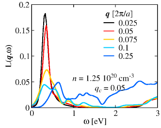
To exemplify the effect of Landau damping on the plasmon dispersion, we illustrate in Fig. 3 the plasmon peak in the loss function of silicon at a doping concentration of cm-3. At these carrier concentration, we obtain a momentum cutoff in units of , with being the lattice constant. For , the loss function exhibit well defined plasmon peak with a peak intensity larger than the continuum of electron-hole excitations. For , on the other hand, the plasmon intensity is reduced as a consequence of the lifetime effects introduced by Landau damping, and its intensity becomes essentially indistinguishable from the spectral signatures of electron-hole pairs.
Appendix C Plasmon-limited mobility
We now evaluate the impact of electron-plasmon scattering processes on the carrier mobility in silicon. In the relaxation-time approximation the mobility is given by , where is the conductivity effective mass, that is the harmonic average of the longitudinal and transverse masses, and is the scattering time arising from processes involving plasmons (eP), phonons (ep), electron-hole pairs (eh), and impurities (i). Noting that scattering time and relaxation time differ by less that 10% at low carrier concentrations Das Sarma and Stern (1985), we follow Matthiessen’s rule to calculate , where , , and are the electron self-energies associated with each interaction.
Strictly speaking the mobility is an average property of all the carriers in a semiconductor; however, for illustration purposes, it is useful to consider a ‘single-electron’ mobility obtained as . This quantity is shown in Fig. 4a. In this figure we see that the mobility decreases as one moves higher up in the conduction band; this behavior relates to the increased phase-space availability for electronic transitions. In addition we see that the mobility decreases with increasing carrier concentration. In order to analyse this trend we give a breakdown of the various sources of scattering in Fig. 4c, and we compare our calculations to experiment. Here we show the carrier mobility at 300 K averaged on the Fermi surface defined by the doping level. Electrical measurements at high doping Mousty et al. (1974) yield mobilities in the range of 100-300 cmV-1s-1 for carrier densities between and cm-3; these data are shown as black circles in Fig. 4b-c. Were we to consider only electron-phonon scattering and electron-hole pair generation, we would overestimate the experimental mobilities by more than an order of magnitude (red and yellow lines in Fig. 4c). Impurity scattering reduces this discrepancy to some extent, but there remains a residual difference at the highest doping levels. It is only upon accounting for electron-plasmon scattering that the calculations exhibit a trend in qualitative and even semi-quantitative agreement with experiments throughout the entire doping range. In particular the scattering by plasmons is key to explain the anomalous low mobility of 100 cmV-1s-1 above cm-3. Even through the inclusion of electron-plasmon scattering a residual discrepancy between theory and experiment is still observed, which we ascribe to the simplified models adopted in the description of electronic scattering with electron-hole pairs and impurities. This observation leads us to suggest that the origin of the mobility overestimation in earlier calculations could be connected with the neglect of electron-plasmon scattering Meyer and Bartoli (1987); Restrepo et al. (2009).
References
- Lal et al. (2007) S. Lal, S. Link, and N. J. Halas, Nat. Photonics 1, 641 (2007).
- Walters et al. (2010) R. J. Walters, R. V. A. van Loon, I. Brunets, J. Schmitz, and A. Polman, Nat. Mater. 9, 21 (2010).
- Atwater and Polman (2010) H. A. Atwater and A. Polman, Nat. Mater. 9, 205 (2010).
- Brongersma et al. (2015) M. L. Brongersma, N. J. Halas, and P. Nordlander, Nat. Nanotechnol. 10, 25 (2015).
- Lukianova-Hleb et al. (2013) E. Y. Lukianova-Hleb, X. Ren, R. R. Sawant, X. Wu, V. P. Torchilin, and D. O. Lapotko, Nat. Med. 20, 778 (2013).
- Zhang et al. (2013) Z. Zhang, J. Wang, and C. Chen, Adv. Mater. 25, 3869 (2013).
- Maier (2007) S. Maier, Plasmonics: Fundamentals and Applications (Springer, 2007).
- Pitarke et al. (2007) J. M. Pitarke, V. M. Silkin, E. V. Chulkov, and P. M. Echenique, Rep. Prog. Phys. 70, 1 (2007).
- Ozbay (2006) E. Ozbay, Science 311, 189 (2006).
- Bohm and Pines (1953) D. Bohm and D. Pines, Phys. Rev. 92, 609 (1953).
- Pines and Schrieffer (1962) D. Pines and J. R. Schrieffer, Phys. Rev. 125, 804 (1962).
- Nozières and Pines (1959) P. Nozières and D. Pines, Phys. Rev. 113, 1254 (1959).
- Adler (1962) S. L. Adler, Phys. Rev. 126, 413 (1962).
- Wiser (1963) N. Wiser, Phys. Rev. 129, 62 (1963).
- Pines (1999) D. Pines, Elementary Excitations in Solids (Perseus, 1999).
- (16) See Supplemental Material at tobeaddedbypublisher, which includes Refs. Hedin (1965); Aulbur et al. (2000); Hybertsen and Louie (1986); Engelsberg and Platzman (1966); Lundqvist (1967); Langreth (1970); Overhauser (1971); Mousty et al. (1974); Das Sarma and Stern (1985); Meyer and Bartoli (1987); Restrepo et al. (2009); Hohenberg and Kohn (1964); Kohn and Sham (1965); Giannozzi et al. (2009); Troullier and Martins (1991); Marini et al. (2009); Noffsinger et al. (2010); Baroni et al. (2001); Mostofi et al. (2008).
- Aw et al. (1991) S. E. Aw, H. S. Tan, and C. K. Ong, J. Phys.: Condens. Matter 3, 8213 (1991).
- Balkanski et al. (1969) M. Balkanski, A. Aziza, and E. Amzallag, Phys. Status Solidi B 31, 323 (1969).
- Zacharias et al. (2015) M. Zacharias, C. E. Patrick, and F. Giustino, Phys. Rev. Lett. 115, 177401 (2015).
- Nozieres and Pines (1958) P. Nozieres and D. Pines, Il Nuovo Cimento (1955-1965) 9, 470 (1958).
- Mahan (2000) G. Mahan, Many-Particle Physics (Springer, 2000).
- Engelsberg and Schrieffer (1963) S. Engelsberg and J. R. Schrieffer, Phys. Rev. 131, 993 (1963).
- Fröhlich (1954) H. Fröhlich, Advances in Physics 3, 325 (1954).
- Verdi and Giustino (2015) C. Verdi and F. Giustino, Phys. Rev. Lett. 115, 176401 (2015).
- Jalabert and Das Sarma (1990) R. Jalabert and S. Das Sarma, Phys. Rev. B 41, 3651 (1990).
- Bernardi et al. (2014) M. Bernardi, D. Vigil-Fowler, J. Lischner, J. B. Neaton, and S. G. Louie, Phys. Rev. Lett. 112, 257402 (2014).
- Doany and Grischkowsky (1988) F. E. Doany and D. Grischkowsky, Appl. Phys. Lett. 52 (1988).
- Marini (2008) A. Marini, Phys. Rev. Lett. 101, 106405 (2008).
- Giustino et al. (2010) F. Giustino, S. G. Louie, and M. L. Cohen, Phys. Rev. Lett. 105, 265501 (2010).
- Cannuccia and Marini (2011) E. Cannuccia and A. Marini, Phys. Rev. Lett. 107, 255501 (2011).
- Botti and Marques (2013) S. Botti and M. A. L. Marques, Phys. Rev. Lett. 110, 226404 (2013).
- Monserrat et al. (2014) B. Monserrat, N. D. Drummond, C. J. Pickard, and R. J. Needs, Phys. Rev. Lett. 112, 055504 (2014).
- Antonius et al. (2014) G. Antonius, S. Poncé, P. Boulanger, M. Côté, and X. Gonze, Phys. Rev. Lett. 112, 215501 (2014).
- Liang and Yang (2015) Y. Liang and L. Yang, Phys. Rev. Lett. 114, 063001 (2015).
- Damascelli et al. (2003) A. Damascelli, Z. Hussain, and Z.-X. Shen, Rev. Mod. Phys. 75, 473 (2003).
- Moser et al. (2013) S. Moser, L. Moreschini, J. Jaćimović, O. S. Barišić, H. Berger, A. Magrez, Y. J. Chang, K. S. Kim, A. Bostwick, E. Rotenberg, L. Forró, and M. Grioni, Phys. Rev. Lett. 110, 196403 (2013).
- Caruso et al. (2015) F. Caruso, H. Lambert, and F. Giustino, Phys. Rev. Lett. 114, 146404 (2015).
- Caruso and Giustino (2015) F. Caruso and F. Giustino, Phys. Rev. B 92, 045123 (2015).
- Bustarret et al. (2006) E. Bustarret, C. Marcenat, P. Achatz, J. Kacmarcik, F. Levy, A. Huxley, L. Ortega, E. Bourgeois, X. Blase, D. Debarre, and J. Boulmer, Nature 444, 465 (2006).
- Ekimov et al. (2004) E. A. Ekimov, V. A. Sidorov, E. D. Bauer, N. N. Mel’nik, N. J. Curro, J. D. Thompson, and S. M. Stishov, Nature 428, 542 (2004).
- Boeri et al. (2004) L. Boeri, J. Kortus, and O. K. Andersen, Phys. Rev. Lett. 93, 237002 (2004).
- Lee and Pickett (2004) K.-W. Lee and W. E. Pickett, Phys. Rev. Lett. 93, 237003 (2004).
- Blase et al. (2004) X. Blase, C. Adessi, and D. Connétable, Phys. Rev. Lett. 93, 237004 (2004).
- Giustino et al. (2007) F. Giustino, M. L. Cohen, and S. G. Louie, Phys. Rev. B 76, 165108 (2007).
- Hedin (1965) L. Hedin, Phys. Rev. 139, A796 (1965).
- Aulbur et al. (2000) W. G. Aulbur, L. Jönsson, and J. W. Wilkins, Solid State Phys. 54, 1 (2000).
- Hybertsen and Louie (1986) M. S. Hybertsen and S. G. Louie, Phys. Rev. B 34, 5390 (1986).
- Engelsberg and Platzman (1966) S. Engelsberg and P. M. Platzman, Phys. Rev. 148, 103 (1966).
- Lundqvist (1967) B. Lundqvist, Phys. Kondens. Mater. 6, 193 (1967).
- Langreth (1970) D. C. Langreth, Phys. Rev. B 1, 471 (1970).
- Overhauser (1971) A. W. Overhauser, Phys. Rev. B 3, 1888 (1971).
- Mousty et al. (1974) F. Mousty, P. Ostoja, and L. Passari, J. Appl. Phys. 45 (1974).
- Das Sarma and Stern (1985) S. Das Sarma and F. Stern, Phys. Rev. B 32, 8442 (1985).
- Meyer and Bartoli (1987) J. R. Meyer and F. J. Bartoli, Phys. Rev. B 36, 5989 (1987).
- Restrepo et al. (2009) O. D. Restrepo, K. Varga, and S. T. Pantelides, Appl. Phys. Lett. 94, 212103 (2009).
- Hohenberg and Kohn (1964) P. Hohenberg and W. Kohn, Phys. Rev. 136, B864 (1964).
- Kohn and Sham (1965) W. Kohn and L. J. Sham, Phys. Rev. 140, A1133 (1965).
- Giannozzi et al. (2009) P. Giannozzi et al., J. Phys.: Condens. Matter 21, 395502 (2009).
- Troullier and Martins (1991) N. Troullier and J. L. Martins, Phys. Rev. B 43, 1993 (1991).
- Marini et al. (2009) A. Marini, C. Hogan, M. Grüning, and D. Varsano, Comp. Phys. Commun. 180, 1392 (2009).
- Noffsinger et al. (2010) J. Noffsinger, F. Giustino, B. D. Malone, C.-H. Park, S. G. Louie, and M. L. Cohen, Comp. Phys. Commun. 181, 2140 (2010).
- Baroni et al. (2001) S. Baroni, S. de Gironcoli, A. Dal Corso, and P. Giannozzi, Rev. Mod. Phys. 73, 515 (2001).
- Mostofi et al. (2008) A. A. Mostofi, J. R. Yates, Y.-S. Lee, I. Souza, D. Vanderbilt, and N. Marzari, Comp. Phys. Commun. 178, 685 (2008).