Superconductivity of niobium thin films in the BiOCl/Nb heterostructures.
Abstract
In the current paper, electrical transport properties of 25 nm thick Nb films sputtered on the photosensitive semiconductor BiOCl were investigated in the8 temperature range 7.5 K 8.5 K. The influence of green (532 nm) and red (640 nm) laser excitations on resistive superconducting transitions of the niobium thin films on a silicon glass and BiOCl single crystal substrates were studied. The temperature dependences of the resistivity for Nb are in good agreement with the McMillan model which indicates the strong influence of the inverse proximity effect induced by the interface. The increased influence of the BiOCl/Nb interface under laser excitation corresponds to the raising the ratio of the density of normal to superconductivity carriers in the limit and this observation is in agreement with the photoconductivity study of BiOCl single crystals.
pacs:
74.25.F- 68.35.bg 74.45.+cI Introduction
In the past decade, attention was paid to the light-induced effect in superconductors Fausti ; Mitrano ; Suda . Under laser excitation, it is possible to manipulate the surface density of state, to change superconducting properties. Another possibility to change the local density of states arises from proximity induced effects Gennes . One can manipulate the superconducting density of states at the interface using photosensitive semiconductor/superconductor heterostructures. Bismuth oxyhalides BiOX (X = F, Cl, Br and I) photosensitive semiconductors that have attracted intensive attention due to their characteristic photoelectrical properties and possible technological applications Wu ; Gondal . Due to their layered structure and facile fabrication by exfoliation Geim , single crystals with thicknesses less than 1 m could be used as a substrate for semiconductor/superconductor heterostructures.
The electrical transport properties of thin Nb films, with nominal thicknesses of 25 nm, supported on Si glass or BiOCl single crystal substrates were investigated in the temperature range 7.5 K 8.5 K with and without laser excitation. The temperature dependences of resistivity for Nb on Si glass overlapping with each other indicating an excellent stability of interface. The resistive curves at the vicinity of superconducting transition for Nb on BiOCl single crystal are in good agreement with the McMillan model mcmillan , which indicates the strong influence of inverse proximity effect induced by the interface. The calculated depth of the interface is approximately 0.85 nm. The increased influence of the interface under the laser excitation corresponds to the raising in ratio ( are the density of states in normal (N) and superconducting (S) layers at = 0). It is in agreement with the photoconductivity spectra of BiOCl single crystals obtained in BundaSAM .
II Experimental details
In this work, a magnetron sputtering technique was used to generate Nb films with nominal thicknesses of 25 nm. Sputtering conditions were: chamber pressure 3.710-10 Pa, argon pressure 310-5 Pa, DC target power 270 W, substrate temperature 22 ∘C. The thickness of the sputtered films was controlled by quartz crystal microbalance device. The films were simultaneously deposited on commercially purchased Si glass slides 20 mm x 20 mm x 0.5 mm and BiOCl single crystal 10 mm x 5 mm x 1 m obtained by exfoliation method Geim . The high-quality BiOCl single crystal that served as the source of the thin films was synthesized using gas transfer methods briefly described in BundaSAM .

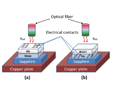
The electrical resistivity of the Nb thin films was obtained by the four-point probe measurements of a direct current using Keithley 6221 current source and Keithley 2182A nanovoltmeter. Temperature control was performed using the commercial Physical Property Measurement System (PPMS). Temperature dependences were obtained in both cooling and heating modes at two temperature rates 0.1 K/min and 0.3 K/min. Thermal contact was established by installing sample on a massive Cu plate glued with the GE-Varnish (see scheme in Fig. 1). Electric contacts were made using the silver conducting paste with annealing at 80oC during 10 min. The thin sapphire plate was used to avoid short circuit or current leaking. Laser excitation with the power 15 mW/cm2 was applied on either Nb (Fig. 1a) or the photosensitive semiconductor BiOCl (Fig. 1b). Laser excitations with 532 nm (2.33 eV) and 640 nm (1.94 eV) were obtained by two CNI laser devices with the maximum power 300 mW and 200 mW, respectively. Output laser power was measured using thermal power sensor (Ophir, 3A-P). Resistive curves were measured at the current 1 A.
III Results and discussion
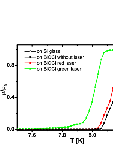
The experimental results of the superconducting transition for the Nb films under various mounting and irradiation conditions are given in Fig. 2. It is noteworthy that the data for the transitions were acquired with warming and cooling protocols at two different rates, and the results for a specific mounting/irradiation conditions were independent of the various measuring conditions. This observation indicates that a high-quality thermal contact exists between the sample and the cold plate of the PPMS, and consequently, the laser excitation does not significantly perturb the temperature of the sample. Only the curves measured at temperature rate 0.1 K/min in cooling mode are plotted in Fig. 2.

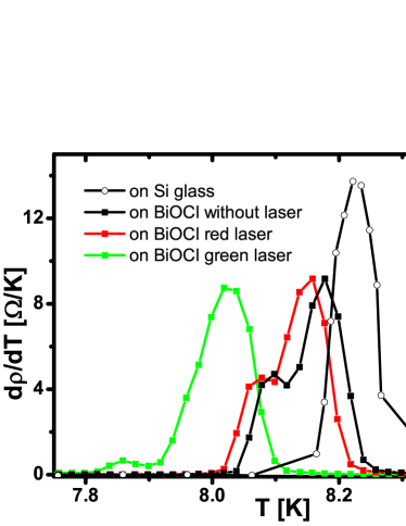
Critical temperatures were identified by the maximum value of curves (fig. 3), and the results are tabulated in Table 1. The width of superconducting transitions was identified in the temperature range from deviation from normal state behavior till the state (Fig. 2). The thin film sputtered on Si glass has a critical temperature 8.2 K along with the width of superconducting transition 0.2 K and the residual resistance ratio (RRR) 4.3 indicates a high quality of the thin film. All measured curves, both without and with laser excitation, perfectly match each other, and this result is a consequence of an interface with excellent stability.

The superconducting transitionss of Nb on the BiOCl substrate shift to the lower temperatures with increasing of the laser excitation energy. The residual resistance ratio measured without laser excitation 3.8, which is slightly lower compared to the Si glass substrate. The higher width of the superconducting transition and the presence of the second, low-temperature peak curves could indicate the phase separation in Nb thin films. With and without irradiation, the RRR for Nb on BiOCl is the same, so the defect concentration is constant during all measurements. On the other hand, the width of the superconducting transition usually indicates the impureness of the sample and this parameter increased sufficiently under laser excitation.
| Conditions | , K | , K | ||
| Si glass | BiOCl | Si glass | BiOCl | |
| Without laser | 8.22 | 8.17 | 0.2 | 0.24 |
| Red light | 8.22 | 8.15 | 0.2 | 0.28 |
| Green light | 8.22 | 8.02 | 0.2 | 0.35 |
Such a behavior could be explained regarding inverse proximity effect Delacour . Despite the good quality of thin films, which indicates in RRR 4, the pure Nb single crystals have RRR up to 2600 Malang . Consequently, the approximation in dirty limit could be used. According to Ashcroft Ashcroft , the electron mean free path was estimated as , where is a sheet resistance in cm and ratio for Nb is equals to 3.07. The experimental value of sheet resistance is = 3.09 cm, which leads to the 28 nm. Since the sample thickness is less than the electron mean free path , the former was used to evaluate the coherence length in the dirty limit Ashcroft as = 0.852. Assuming = 38 nm for bulk Nb Delacour , then this analysis yields = 26 nm. This value is very close to the thickness of our Nb film = 25 nm and places our study in the two-dimensional limit. According to the McMillan model mcmillan , the inverse proximity effect in a planar thin film geometry is an appropriate description of our experimental conditions. Consequently, the critical temperature is suppressed by the normal state interface with the thickness described by the equation:
| (1) |
where = 277 K is the Nb Debye temperature, = 9.22 K is the Nb bulk critical temperature Delacour and . Considering a without laser excitation, the calculated values of estimated as 0.85 nm. Under the laser excitation, the only parameter in eq. (1) being changed is . Consequently, increasing of the ratio leads to the suppression of the superconductivity. Changes for ratio are 1.02 under the red light excitation and 1.15 under the green light excitation. Such behavior is in good agreement with photoconductivity spectra obtained in BundaSAM for BiOCl single crystals.
IV Conclusions
The electrical transport properties of 25 nm Nb thin films were investigated in a temperature range 7.5 K 8.5 K on Si glass and BiOCl substrates with and without laser excitation. Resistive curves with and without laser excitation for Nb on Si glass matched with each other which indicates a good stability of interface and parameters in eq. (1). The temperature dependences of resistivity of Nb on BiOCl single crystal are in good agreement with the McMillan model which indicates the strong influence of inverse proximity effect induced by the interface. The calculated depth of the normal state interface is 0.85 nm. The increased influence of the interface under the laser excitation corresponds to the enlarging in ratio which is in agreement with the photoconductivity study of BiOCl single crystals.
V Acknowledgements
This work was supported by the ERDF EU (European Union European regional development fond) grant, under the contract No. ITMS 26220120005, ITMS 26220220186, APVV 0605-14 and VEGA 1-0409-15. We thank prof. M. W. Meisel for the fruitful discussions and comments that improved the manuscript.
References
- (1) D. Fausti, R. I. Tobey, N. Dean, S. Kaiser, A. Dienst, M. C. Hoffmann, S. Pyon, T. Takayama, H. Takagi and A. Cavalleri, Science 331, 189 (2011) DOI: 10.1126/science.1197294
- (2) M. Mitrano, A. Cantaluppi, D. Nicoletti, S. Kaiser, A. Perucchi, S. Lupi, P. Di Pietro, D. Pontiroli, M. Ricco, S. R. Clark, D. Jaksch and A. Cavalleri, Nature 530, 461 (2016) DOI: 10.1038/nature16522
- (3) M. Suda, R. Kato and H. M. Yamamoto, Science 347, 743 (2015) DOI: 10.1126/science.1256783
- (4) P. G. de Gennes, Rev. Mod. Phys. 36, 225 (1964) DOI: 10.1103/RevModPhys.36.225
- (5) S. J. Wu, C. Wang, Y. F. Cui, T. M. Wang, B. B. Huang, X. Y. Zhang, X. Y. Qin, P. Brault, Mater. Lett. 64, 115 (2010) DOI: 10.1038/nmat1849
- (6) M. A. Gondal, X. F. Chang, M. A. Ali, Z. H. Yamani, Q. Zhou, G. B. Ji, Appl. Catal. A: General 397, 192 (2011) DOI: 10.1016/j.apcata.2011.02.033
- (7) A. K. Geim and K. S. Novoselov, Nature Materials 6, 183 (2007) DOI: 10.1038/nmat1849
- (8) W. L. McMillan, Phys. Rev. 175, 537 (1968) DOI: 10.1103/PhysRev.175.537
- (9) V. Bunda and S. Bunda, Superconductors its Properties, Technology, and Applications, 323 (2012) ISBN: 978-953-51-0545-9
- (10) C. Delacour, L. Ortega, M. Faucher, T. Crozes, T. Fournier, B. Pannetier and V. Bouchiat, Phys. Rev. B 83, 144504 (2011) DOI: 10.1103/PhysRevB.83.144504
- (11) E. U. Malang, C. S. Oglesby, T. Siegrist and E. Bucher, Physica B: Condensed Matter 204, 363 (1995) DOI: 10.1016/0921-4526(94)00288-7
- (12) N. W. Ashcroft and N. D. Mermin, Solid State Physics (Holt, Rinehart and Winston, New York 1976) ISBN: 0-03-083993-9