Performance of Edgeless Silicon Pixel Sensors on p-type substrate for the ATLAS High-Luminosity Upgrade
Abstract
In view of the LHC upgrade phases towards the High Luminosity LHC (HL-LHC), the ATLAS experiment plans to upgrade the Inner Detector with an all-silicon system.
The n-on-p silicon technology is a promising candidate to achieve a large area instrumented with pixel sensors, since it is radiation hard and cost effective.
The paper reports on the performance of novel n-on-p edgeless planar pixel sensors produced by FBK-CMM, making use of the active trench for the reduction of the dead area at the periphery of the device. After discussing the sensor technology an overview of the first beam test results will be given.
Index Terms:
Silicon pixel sensors, edgeless sensors, radiation detectors, HL-LHC trackerI Introduction
The ATLAS collaboration will upgrade the current Pixel Detector [1] in two phases. A first upgrade has already been realised during the shut-down in 2013-14, by inserting a fourth detection layer (Insertable B-Layer - IBL [2] ) at a radius of 3.2 cm from the beam line. Beyond 2023, the Phase-II luminosity upgrade for the LHC, aims to increase the instantaneous luminosity to cm-2 s-1, posing a serious challenge to the technology for the ATLAS tracker in the High Luminosity era (HL-LHC): the lifetime fluence for the innermost layer, including safety factors, is estimated to be on the order of neq/cm2 [3]. Hence, in view of a possible pixel system replacement after 2023, new pixel sensors are under study. Within the Planar Pixel Sensor collaboration (PPS) [4] several optimizations of the well-known silicon planar technology are under investigation.
The new pixel sensors will not only have to sustain the harsher environment, but also have to show high geometrical acceptance without overlapping adjacent modules. Hence the inactive area has to be reduced significantly. One way to reduce or even eliminate the insensitive region along the device periphery is offered by the “active edge” technique [5], in which a deep vertical trench is etched along the device periphery throughout the entire wafer thickness, thus performing a damage free cut (this requires using a support wafer, to prevent the individual chips from getting loose). The trench is then heavily doped, extending the ohmic back-contact to the lateral sides of the device: the depletion region can then extend to the edge without causing a large current increase.
The active edge technology has been chosen for a first production of n-on-p planar sensors at FBK. Studies performed with TCAD simulation tools helped in defining the layout and making a first estimation of the charge collection efficiency expected after irradiation [6].
In this paper an overview of the performance of novel edgeless silicon n-on-p planar pixel sensors fabricated at FBK-CMM [6] is presented. The sensors have been produced on 4” wafer of high resistivity Float zone (Fz) material, with a thickness of , by making use of the active trench concept [5]. This technology requires a single-sided process, featuring a doped trench, extending all the way through the wafer, and completely surrounding the sensor (see Fig.1) The presence of a support wafer was then required.
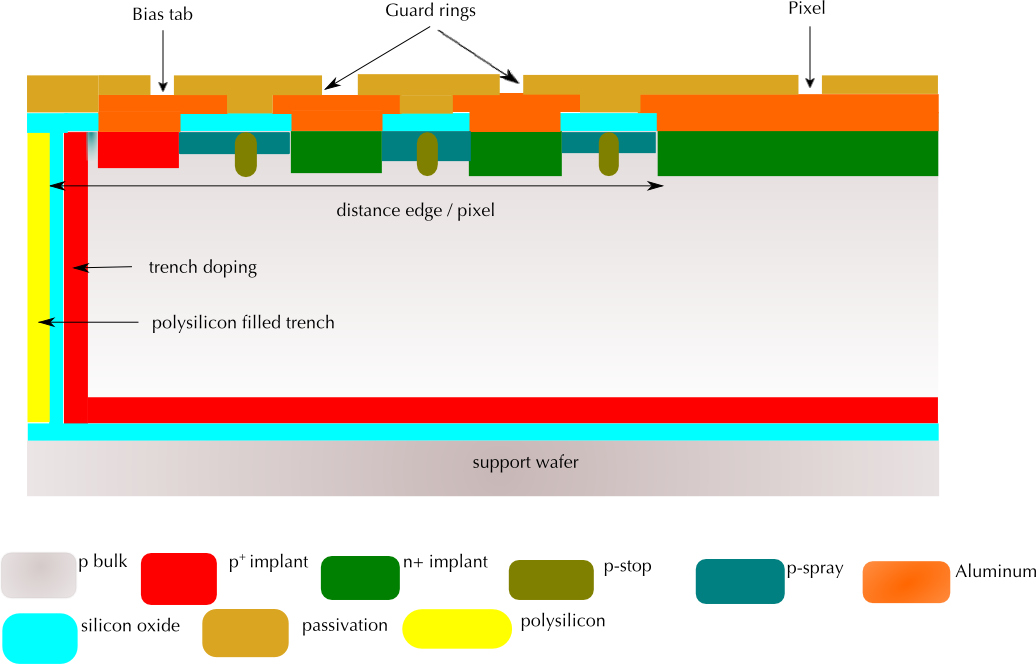
The wafer layout contains nine ATLAS FE-I4 [7] compatible pixel sensors with different number of guard-rings - GRs - (0, 1, 2, 3, 5 and 10) and different pixel-to-trench distances (100, 200, 300 and 400 m) in order to evaluate the best sensor configuration (see Table I). In addition, several test-structures have been also implemented to study the electrical behaviour of an even larger number of GRs and pixel to trench distances combination.
| # of GRs | pixel-to-trench distance () |
| 0 | 100 |
| 1 | 100 |
| 2 | 100 |
| 3 | 200 |
| 5 | 300 |
| 10 | 400 |
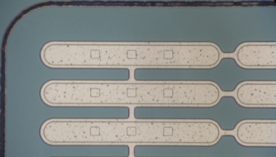
In Figure 2 the edge area of a test structure is reported; this test structure featured FE-I4-like pixels. The black line sourrinding the pixels’ electrodes is the doped trench; the distance between the trench and the pixels’ electrodes is 100 m, and, as it can be seen, there are no guard-rings.
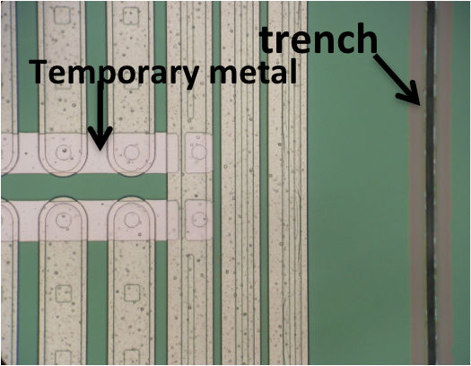
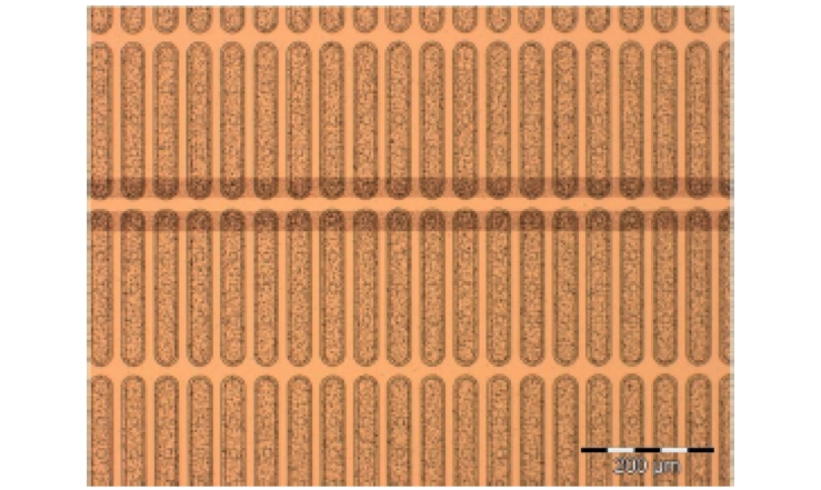
Since some sensors were to be bump-bonded to FE-I4 read-out chips, it was necessary to select good sensors at the wafer level, by measuring their I-V characteristics. For this purpose, an additional layer of metal was deposited over the passivation and patterned into stripes, each of them shorting together a row of pixels, contacted through the small passivation openings foreseen for the bump bonding. This solution has already been adopted for the selection of good 3D FE-I4 sensors for the ATLAS IBL [8]. After the automatic current-voltage measurement on each FE-I4 sensor, the metal was removed by wet etching, which does not affect the electrical characteristics of the devices.
In Figure 3 a sensor before and after the temporary metal removal is reported.
II 2015 DESY testbeam results
In march 2015 one FE-I4 pixel module was tested on beam at DESY [9]. The module has been realized by bump-bonding one FE-I4B [7] readout chip and one active edge pixel sensor from our n-on-p production; the sensor had 100 m pixel-to-trench distance and no GRs; it can be said that for what concerns the edge region this sensors looked as the one in Figure 2. In what follows this pixel module under test will be reffered to as LPNHE5.
In DESY the measurements were performed on beamline 21 [9]. Electrons of 4 GeV/c momentum where impinging normally to our LPNHE5 module surface. The LPNHE5 device under test (DUT) was placed between the two arms of the DATURA beam telescope [10].
Several configurations were tested, including different bias voltage values for the DUT and different threshold values for the FEI4 readout chip; data were recorded too when the normal to the DUT was making an angle of 15∘ with respect to the beam axis. All measurements were performed at room temperature.
In Figure 4 a picture of the setup.
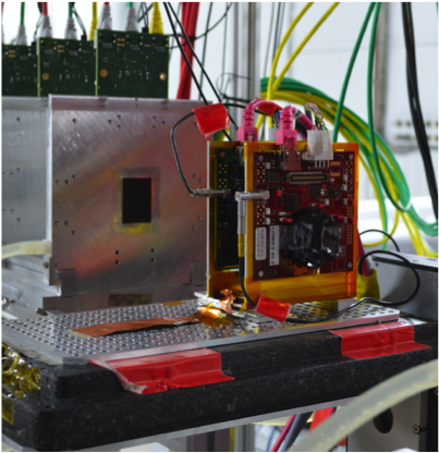
A trigger signal was generated by the coincidence of 2 scintillators pairs, one upstream and one downstream of the telescope. The data acquisition rate was limited to Hz by some data acquisition problems.
Data were reconstructed using the eutelescope/eudaq software [11] and analysed with the tbmon2 package [12]. Tracks were built from clusters of hits in the telescope planes. An iterative alignment fit procedure, followed by a tracks fit step allowed to obtain a pointing resolution of about 3 m, thanks also to the telescope planes pixel sensor small pitch (m) [13].
Once a set of good tracks was defined, the clusters properties, the hit-efficiency and the spatial resoultion of the LPNHE5 DUT were studied.
II-A Cluster properties
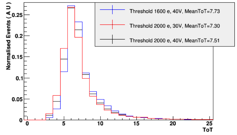
Clusters were formed by grouping neighboring pixels that fired in time with tracks registred by telescope. For tracks at normal incidence about 20% of the clusters were composed by more than one pixel; for tracks at 15∘ more than 60% of the clusters were composed by two or more pixels. In Figure 5 the cluster charge, measured as Time-over-Threshold (ToT), is shown. As expected, lower threshold and higher bias voltage 111The depletion voltage was 20 V. gives the cluster more charge.
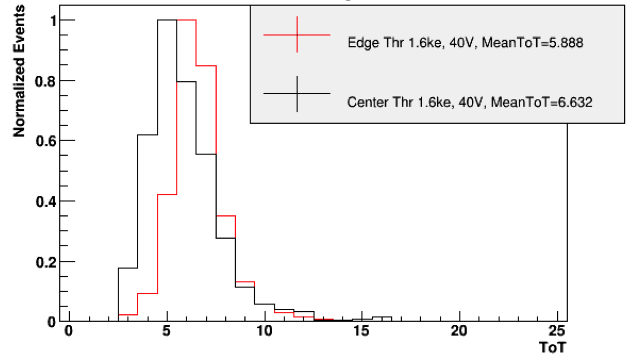
Edge pixels properties were studied, first of all to check if they show the same performance as the “central” ones. In Figure 6 the charge measured by isolated single pixels is presented, separately for the edge and the center zone. It can be seen that edge pixels are at least as effective as the central ones in collecting charge; they are actually collecting more charge on average and this can be explained by charge collection from the un-instrumented area which hence is active. This is a first strong indication that the active edge technology works.
II-B Hit-efficiency
The LPNHE5 hit-efficiency performance has been studied by looking at hits on the DUT close to the extrapolated track impact position. Table II reports the hit efficiency 222hit efficiency errors are negligible for the different tested configuration.
| bias (V) | threshold (ke) | efficiency (%) |
|---|---|---|
| 30 | 2.0 | 98.4 |
| 40 | 2.0 | 98.7 |
| 40 | 1.6 | 99.1 |
The hit efficiency is always above 98%; it is better than 99% for the best configuration (40 V bias voltage and 1.6 ke threshold ). This is a remarkable result: even at moderate bias voltage the detector is full efficient.
In Figure 7 the so-called “in-pixel” hit efficiency is shown for 40 V bias voltage and 1.6 ke threshold. All the pixels have been superimposed in order to study the hit-efficiency as a function of the track impact point.
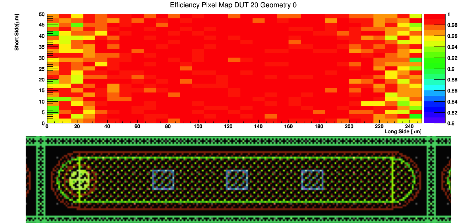
As it can be seen the efficiency is very uniform across the pixel cell, above 95% everywhere. The fact that after the temporary metal removal there were no biasing structures left made the cell very effective everywhere. A small less efficient region is visible at the corners of the cell; this is due to charge sharing with the nieghbouring cells.
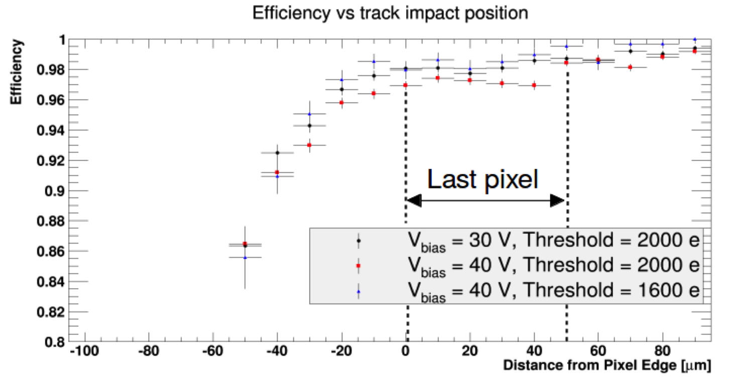
To completely validate the active edge approach the hit-efficiency at the sensor edge had to be measured. The results are shown in Figure 8. The efficiency is measured as a function of the track impact point for the row of pixels closest to the trench. Points with abscissa lower than 0 correspond to tracks passing in the volume within the pixels and the trench. It can be seen that the hit-efficiency is still above 90% for all configurations even 40 m away from the last pixel implant 333there are no usable tracks beyond -50 m. This result represents the validation of the active edge approach: the un-instrumented volume is active and highly efficient.
II-C Spatial resolution
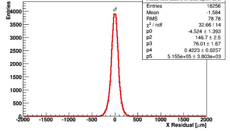
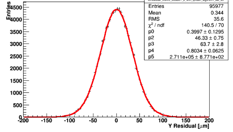
To evaluate the spatial resolution of the LPNHE5 module the hit-residuals, defined as the reconstructed hit position minus the track impact position, were studied. The hit-residual distributions for the long (250 m) and short (50 m) pixel directions are presented in Figure 9. The analysis is strongly limited by the multiple scattering effect, estimated to be of the order of 30 m. The RMS values of the hit-residual distributions for the long and short pixel directions are m and m, respectively; the results are consistent with the expectations.
III Conclusions
In this paper we reported the performance of thin n-on-p pixels aimed at the HL-LHC phase of ATLAS. These pixels are characterized by their reduced un-instrumented area at the detector periphery. This was possible thanks to the active edge technology.
The testbeam results showed that our detector has a very high hit efficiency, very uniform across the detector. It was also shown that the pixels at the detector edge collect charge from the un-instrumented volume as well. More important, the detector is very effective also well beyond the pixels area.
Acknowledgment
We thank the ITk pixel testbeam members that contributed to make these measurements possible
Thanks to A. Macchiolo, N. Savic and S. Terzo from MPI for useful discussion. We thank CERN for letting us use their laboratory.
This work was supported in part by the Autonomous Province of Trento, Project MEMS2, and in part by the Italian National Institute for Nuclear Physics (INFN).
The measurements leading to these results have been performed at the Test Beam Facility at DESY Hamburg (Germany), a member of the Helmholtz Association (HGF).
References
- [1] G. Aad, M. Ackers, F. Alberti, M. Aleppo, G. Alimonti et al., “Atlas pixel detector electronics and sensors,” JINST, vol. 3, p. P07007, 2008.
- [2] ATLAS IBL Community, “Atlas insertable b-layer technical design report,” CERN, Tech. Rep., 2010. [Online]. Available: http://cdsweb.cern.ch/record/1291633/files/ATLAS-TDR-019.pdf
- [3] S. McMahon, P. Allport, H. Hayward, and B. Di Girolamo, “Initial Design Report of the ITk: Initial Design Report of the ITk,” CERN, Geneva, Tech. Rep. ATL-COM-UPGRADE-2014-029, Oct 2014. [Online]. Available: https://cds.cern.ch/record/1952548
- [4] C. Nellist, “Achievements of the atlas upgrade planar pixel sensors r&d project,” Journal of Instrumentation, vol. 10, no. 01, p. C01027, 2015. [Online]. Available: http://stacks.iop.org/1748-0221/10/i=01/a=C01027
- [5] C .J Kenney et al., “Results from 3-d silicon sensors with wall electrodes: Near-cell-edge sensitivity measurements as a preview of active-edge sensors,” IEEE Transactions on Nuclear Science, , vol. 48, no. 6, pp. 2405–2410, 2001.
- [6] M. Bomben et al., “Development of Edgeless n-on-p Planar Pixel Sensors for future ATLAS Upgrades,” Nucl. Instr. and Meth. A, vol. 712, pp. 41–47, 2013.
- [7] M. Garcia-Sciveres et al., “The fe-i4 pixel readout integrated circuit,” Nucl. Instr. and Meth. A, vol. 636, pp. S155–S159, 2011.
- [8] G. Giacomini, A. Bagolini, M. Boscardin, G.-F. Dalla Betta, F. Mattedi, M. Povoli, E. Vianello, and N. Zorzi, “Development of double-sided full-passing-column 3d sensors at fbk,” Nuclear Science, IEEE Transactions on, vol. 60, no. 3, pp. 2357–2366, 2013.
- [9] testbeam.desy.de. [Online]. Available: testbeam.desy.de
- [10] A. Bulgheroni, “Results from the EUDET telescope with high resolution planes,” Tech. Rep. EUDET-Report-2009-02, 2009.
- [11] http://eutelescope.web.cern.ch/. [Online]. Available: http://eutelescope.web.cern.ch/
- [12] https://bitbucket.org/TBmon2/tbmon2/overview. [Online]. Available: https://bitbucket.org/TBmon2/tbmon2/overview
- [13] C. Hu-Guo et al., “First reticule size MAPS with digital output and integrated zero suppression for the EUDET-JRA1 beam telescope,” Nucl. Instrum. Methods Phys. Rev. A, vol. 623, no. 1, pp. 480 – 482, 2010, 1st International Conference on Technology and Instrumentation in Particle Physics.