Infrared photodetectors based on graphene van der Waals heterostructures
Abstract
We propose and evaluate the graphene layer (GL) infrared photodetectors (GLIPs) based on the
van der Waals (vdW) heterostructures with the radiation absorbing GLs.
The operation of the GLIPs is associated with the electron photoexcitation
from the GL valence band to the continuum states above the inter-GL barriers
(either via tunneling or direct transitions to the
continuum states). Using the developed device model, we calculate the photodetector characteristics as functions of the GL-vdW heterostructure parameters.
We show that due to
a relatively large efficiency of the electron photoexcitation and low capture efficiency of the electrons propagating over the barriers in the inter-GL layers, GLIPs should exhibit the
elevated photoelectric gain and detector responsivity as well as relatively high detectivity.
The possibility of high-speed operation, high conductivity, transparency of the GLIP contact layers, and the sensitivity to normally incident IR radiation
provides additional potential advantages in comparison with other IR photodetectors.
In particular, the proposed GLIPs can compete with unitravelling-carrier photodetectors.
Keywords: graphene, van der Waals heterostructure, infrared photodetector
I Introduction
Successful development of the van der Waals (vdW) heterostructures 1 based on stacking of two-dimensional (2D)
crystals and graphene layers (GLs) promises a significant progress in infrared (IR)
and terahertz (THz) optoelectronics
2 ; 3 . The unique properties of GLs
provide an opportunity to
create new effective photodetectors operating in a wide range of photon energies
4 ; 5 ; 6 ; 7 ; 8 ; 9 ; 10 ; 11 ; 12 ; 13 . Supplementing their design by the band structure engineering using 2D-materials for the barrier layers opens up new prospects in further enhancement of the detector performance.
Recently, new IR and THz detectors using GL-vdW heterostructures were proposed and
evaluated:
(i) THz photodetectors based on a double-GL structure, in which the intraband inter-GL
resonant transitions are assisted by IR or THz photons 14 . The resonant nature of such transitions, in which the electron momentum is conserved 15 ; 16 ; 17 ; 18 ; 19 , promotes their elevated probability
and, hence, the elevated quantum efficiency. These photodetectors require inclined radiation incidence or a radiation coupler (grating structure);
(ii) THz and IR photodetectors based on the GL-vdW heterostructures using the photon-assisted interband
transitions between the neighboring GLs 20 ;
(iii) THz detectors based on the GL-vdW heterostructures operating as hot-electron bolometers using the effect of the emission from GLs of the electrons, heated by the THz
radiation, due to the intraband (Drude) absorptions in GLs 21 .
In this paper, we propose and evaluate the IR photodetectors based on the GL-vdW heterostructures with different numbers of the active undoped GLs placed between the emitter and collector and separated by the inter-GL barriers (GLIPs). These photodetectors are using the interband photoexcitation of the electrons in GLs from the valence band states to the exited states slightly below or higher than the barrier edge. The photoexcited electrons transfer (by tunneling through the barrier top or directly) to the continuum states above the barrier and propagate through the barrier layers. The GL-vdW double-GL photoconductive device with the emitter and collector GLs separated by the barrier and using a similar mechanism was recently proposed 22 fabricated and measured 23 . However, as we demonstrate below, the insertion of the inner GLs, which provides the extra electron photoemission and capture, can lead to a dramatic increase in the GLIP responsivity. This is due to the photocurrent gain associated with the redistribution of the electric field in the heterostructure and leading to amplification of the electron injection from the emitter. Thus the GLIPs in some sense resemble quantum-well infrared photodetectors (QWIPs) typically using III-V materials and extensively studied, fabricated, and used in applications during two decades 24 ; 25 ; 26 ; 27 . Such a similarity is due to the propagation of the photoexcited electrons over the barriers with their fraction being captured back to the bound states (in GLs and QWs, respectively). A relatively low capture probability results in the elevated values of the detector responsivity. Apart from this, in both GLIPs and QWIPs the detector detectivity increases with an increasing number of GLs and QWs (see, for example, 24 ).
The main difference between the GLIPs and QWIPs is in the use of the interband (in GLIPs) and intraband (in QWIPs) transitions. This allows eliminating the grating structures required in the n-QWIPs for radiation coupling. In realistic GLIPs with a relatively large conduction band off-set, the proper electron photoexcitation requires higher photon energies than in QWIPs. This implies that the GLIPs might generally operate at shorter radiation wavelengths than the QWIPs. However, modifying the shape of the barriers by doping of the inter-GL layers, one can achieve an effective electron photoescape at fairly low photon energies (in far-IR range). As shown in 28 ; 29 , the probability of the electron capture into the GLs can be much smaller than that for the QWs (see, for example, 30 ) since doping of the QWs in the QWIPs leads to the inclusion of the electron-electron scattering mechanism of the capture. Smaller capture efficiency is beneficial for a higher detector responsivity 30 (see also, 24 ; 25 ; 26 ; 27 ).
The absence of the GL doping promotes lower electron emission of the thermalized electrons than that in the doped QWs and, hence, leads to a smaller dark current. Finally, the probability of the electron photoexcitation from the GLs is substantially higher than from the QWs. These GLIP features (the sensitivity to the normally incident radiation and higher photoexcitation and lower capture probabilities) provide potential advantages of the GLIPs over the QWIPs and some other photodetectors. The photodetectors based on GL-vdW heterostructures with the tunneling transparent inter-GL barrier layers considered recently 20 and the GLIPs with relatively thick layers studied in the present paper are analogous. However their operation principles are quite different: the photo-stimulated cascade tunneling between GLs in 20 and the photoexcitation of electrons to the continuum states and propagation in GLIPs. In the latter device, only a small fraction of the propagating electrons can be captured to the GLs. Such a distinction results in different spectral properties and other detector characteristics. In particular, in the GLIPs under consideration, the photoexcitation probability can be much larger than the probability of the inter-GL photo-stimulated transfer. This is due to the diminished wave function overlap in the neighboring GLs 20 . Apart from this, the GLIPs considered here and the hot-electron GLIPs using the bolometric mechanism 21 are characterized by a rather low capture probability of electrons in the continuum states 28 ; 29 . This promotes high values of the detector responsivity 30 ; 31 This is in contrast with the detection mechanism associated with the cascade inter-GL photo-stimulated tunneling. The spectral ranges of the photodetectors using the inter-GL photo-stimulated cascade transfer 20 and the electron heating 21 from one side and the spectral range of the GLIP operation can be essentially different. One important feature of the GLIPs is that their operation do not require the mutual alignment of the GLs.
Various device models used for studies of the vertical electron transport in QWs (and GLs) introduce the concept of an ”ideal” emitter (which provides as many injected electrons as the bulk of the structure ”requires”). In the framework of this concept, the electric-field distributions are assumed to be uniform. A more accurate consideration of the transport phenomena in such structures (including GLIPs) in the dark conditions and under irradiation accounts for the self-consistent electric field distributions and the nonideality of the emitter 32 ; 33 ; 34 ; 35 ; 36 ; 37 ; 38 . This paper uses this more accurate approach.
The paper is organized as follows. In Section 2, we describe the possible GLIP device structures and the GLIP operation principle. Section 3 deals with the device mathematical model. The latter includes the equation for the self-consistent electric potential and the equations governing the electron balance in the GLs. In the latter equation, the electron capture into the GLs is described phenomenologically invoking the concept of the capture parameter 30 (see, also, 26 ; 27 ; 28 ; 29 ; 30 . In Section 4, we derive the dark current in the GLIPs as a function of the structural parameters and the applied voltage using the model described in Sec. 3. In Section 5, we calculate the photocurrent (the variation of the current under the incident radiation). The expressions obtained in Sections 4 and 5 are then used in Sec. 6 for the derivation of the GLIP detector responsivity, photoelectric gain, and detectivity. In Section 6, we compare the GLIPs with some other IR photodetectors. In the Conclusion section, we draw the main results of the paper. In the Appendix, we discuss some simplifications of the main model.
II Device structure and operation principle
We consider the GLIPs based on the GL heterostructure which consists of the inner GLs clad between the barrier layers with the top and bottom contact GLs. The conduction band offsets between the emitter GL and the barrier layer, , as well as between the inner GLs and the barrier layers between them, , are smaller than the pertinent offsets in the valence band. Generally, the materials of the emitter barrier layer and of other barrier layers can be different, so that .
The top and bottom GLs are assumed to be doped to provide their sufficiently high lateral conductivity. These extreme GLs serve as the tunneling emitter (injecting electrons into the GL-heterostructure bulk) and the collector, respectively. The top and bottom GLs are supplied with contacts between which the bias voltage is applied. We consider the GL heterostructures with either the n-type or p-type doping of both the emitter and collector GLs and undoped inner GLs and the barrier layers, i.e., the heterostructures with different types of the emitter and collector can also be treated in the framework of our model. The applied voltage in such heterostructures, stimulates the electron tunneling through the barriers with triangular tops. The thermalized electrons tunneling from the GLs and the electrons excited by the incident IR radiation propagate over the barriers.
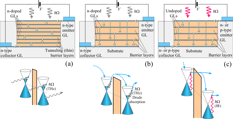
Figures 1(a) and 1(b) show schematically the GLIPs based on GL-vdW heterostructures considered in 20 ; 21 and their band diagrams. Figure 1(c) corresponds to the GLIPs with the bound-to-continuum tunneling and photon-assisted transitions considered in the present work.
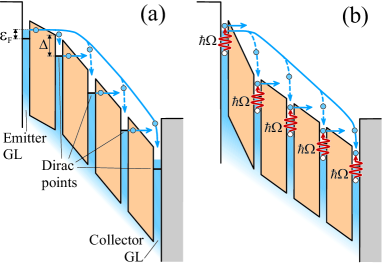
Figure 2 shows the band diagrams of the GLIP (with the structure of figure 1(c)) using the interband intra-GL photoexcitation with the sequential tunneling of the photoexcited electrons (a) in dark conditions and (b) under the strong IR irradiation at the sufficiently high bias voltage (, where is the electron charge and is the temperature in the energy units).
The applied voltage induces the extra carriers of the opposite signs and changes the electron Fermi energies in the emitter and collector GLs. The electron Fermi energies, and , in these GLs (at their equal doping) are different: and Here is the Fermi energy in the extreme GLs at their donor (upper sign for the n-type contact GLs) or acceptor (for the p-type contact GLs) density equal to , is the Planck constant, cm/s is the electron and hole velocity in GLs, and and . Hence, the bias voltage can to some extent affect the emitter injection characteristics decreasing the electron activation energy in the emitter (see the Appendix).
To enhance the electron collection by the collector, the bottom GL can be replaced by a doped multiple-GL or by a thick wider band-gap doped collector region. In principle, the GLIPs with the n-type emitters can be supplied with p-type collectors and vice versa.
The operation of the GLIPs with the device structure and the band diagrams corresponding to figures 1(c) and 2 considered below is associated with the following. The incoming IR photons generate the electron-hole pairs (due to the photon absorption and the vertical interband transitions) in each GL. Depending on the ratio , the photogenerated electrons appear in the continuum states above the barriers directly (if ) or via the intermediate excited state with the energy with respect to the Dirac point following the electron tunneling through the triangular barrier top 39 [see figure 2(b)]. Upon the photoexcitation to the states over the barriers, the electrons propagate toward the collector. During the electron transport over the barrier, a fraction of the propagating electrons is captured into the GLs.
Since we consider devices with the barriers, in which the conduction band off-set and the quantity are smaller than the valence band off-set, the escape of the photogenerated holes from the GLs can be neglected. The GLIP barriers in the devices under consideration can be made of the van der Waals structures with the InSe, WS2, and other barrier layer materials 1 ; 2 ; 16 ; 39 .
III Equations of the model
The Poisson equation governing the electric potential distribution in the direction perpendicular to the GL plane (the direction) and the equations governing the electron balance in each GL at the steady-state irradiation are presented in the following form:
| (1) |
| (2) |
Here and are the 2D densities of electrons and holes in the inner GLs with the index ( and corresponding to the emitter and collector GLs, respectively), is the density of the electron current across GLs, is the capture efficiency for the electrons crossing the GL 25 ; 26 ; 27 ; 28 , and are the rates of the tunneling emission of the thermalized electrons and the tunneling emission of the electrons photoexcited (photogenerated) from the GL valence band in the th GL, is the probability of the interband photon absorption in GLs, ( is the fine structure constant, where is the speed of light in vacuum and is the barrier material refraction index), is the probability of the photoexcited electrons tunneling escape from the th GL to the continuum states above the inter-GL barriers, is the IR radiation intensity (photon flux inside the heterostructure), and are the thickness of the inter-GL barrier layer and its dielectric constant, respectively, and is the Dirac delta function (which reflects narrow localization of the electron and hole charges in the GLs), In contrast to QWIPs using the intraband transitions, the photoexcitation rate in GLIPs is virtually independent of . Both thermalized electron tunneling rate and the escape probability of the photoexcited electrons from the -th GL (and, hence, the photoemission rate) can markedly, namely, exponentially increase with the electric field in the barrier under this GL . The escape probability of the photoexcited electrons is also determined by the effective energy of the photoexcited electron . Although the parameter characterizing the capture into the -th GL depends, to some extent, on the local electric field, this dependence is much weaker than the field-dependence of the tunneling from the GLs. In reality, is most likely to be a functional of the electric-field spatial distribution 26 ; 27 ; 36 . This is particularly true if the energy relaxation length is larger or comparable with the heterostructure thickness . The dependence versus is smoothly decreasing with (see, the previous calculations 26 ). Hence, in the simplest approach can be presented as a function of the average field (in fact, of the bias voltage) as assumed in the following. In line with this, we set , where is a function of .
The tunneling rates of the thermalized and photoexcited electrons (neglecting the intraband Drude absorption in the emitter GL due to relatively high energies of IR photons) can be presented as
| (3) |
| (4) |
Here is the field characterizing the tunneling through the triangular barrier top 40 ; 41 (see also 22 ; 23 ), is the electron mass in the barrier material, is the maximum current density which can be extracted from an undoped GL () at a given temperature, is the try-to-escape time, is the characteristic time of the photoexcited electrons energy relaxation, and if and if . The factor accounts for the difference in the tunneling transparency of the thermalized and photoexcited (with the energy ) electrons. Assuming eV and ( is the free electron mass), we obtain V/m.
At , the right-hand side of equation (3) corresponds to (i.e., the majority of the photogenerated electrons leaves the GLs. In the opposite case , . The energy relaxation of photoexcited electrons in the GL-structures under consideration can be associated with (i) the emission of optical phonons with the transition of an electron to a low energy state in the GL conduction band (at , where eV is the optical phonon energy), (ii) the electron recombination assisted by the emission of optical phonon (when , and (iii) the collisions of the photoexcited electrons with the thermal electrons and holes (in a wide range of IR photon energies . According to the above, one can set
| (5) |
Here is the time of spontaneous optical phonon emission in GLs and is the time of the photoexcited electrons relaxation on the thermalized electrons (and holes) in the GLs. The latter is much shorter in both undoped and doped GLs (see, for example, 40 ). In the following we assume that considering only the mechanism (iii). Since depends on the electron density, we distinguish in the emitter GL and in the inner GLs. As demonstrated in the Appendix, . Although the ratio can be estimated for the heterostructures with different barrier layers, we will mainly considered is as a phenomenological parameter.
In equation (3), we have neglected the thermionic emission from the GLs. The pertinent contribution is proportional to the factor . The latter is assumed to be small compared with the factor in equation (3) at the actual values of the electric field in the barriers and K and lower.
Equation (1) is supplemented by the following boundary conditions:
| (6) |
The current density is equal to the density of the current injected from the emitter GL through a pertinent barrier. Considering both the injection of the thermalized electrons from the doped emitter GL and the escape of the electrons photoexcited in this GL, one can use the following formula relating this current density and the electric field :
| (7) |
Here is the work function from the emitter to the barrier layer normalized by the conduction band offset. The factor is associated with an increase of the thermalized electron density by the electric field in the emitter barrier layer in the GLIPs with the -type emitter layer (see the Appendix). One needs to stress that the value of in the GLIPs with the emitter GL of p-type is larger whereas is smaller () then those for the GLIPs with the n-type emitter GL (due to different signs of the Fermi energy counted with respect to the Dirac point) .
IV Dark current characteristics
In the absence of irradiation (), the current across the GLIP constitutes the dark current, so that . As follows from equations (2), (3), and (7),the electric fields in the barriers are the following functions of the dark current density:
| (8) |
in the near emitter barrier (), and
| (9) |
in other barriers (). Taking into account conditions (6) and using equations (8) and (9), we obtain
| (10) |
Equation (10) yields the following expression for the dark current-voltage characteristics
| (11) |
where .
From equation (11) we obtain
| (12) |
Here the quantity
| (13) |
changes from if to at . Hence is rather smooth function of .
Consequently, at moderate voltages , corresponding to the most practically interesting conditions when the dark current is small,
| (14) |
| (15) |
It is instructive that, according to equation (12), being proportional to strongly increases with decreasing capture efficiency , particularly if (i.e., at . This implies that at sufficiently small when , the net dark current can exceed the current of the tunneling thermalized electrons (which is approximately proportional to the number of inner GLs ), i.e., the main component of the dark current is associated with the current injected from the emitter controlled by the tunneling from the internal GLs being, certainly, smaller than . Another feature of the GLIP current-voltage characteristics and the electric-field spatial distributions given by equations (12) - (14) is their weak dependence on the parameters of the emitters and (at and particularly when ). The latter says that if , the tunneling emitter under consideration can be considered as an ideal.
One needs to stress that due to a decreasing voltage dependence of the capture efficiency , this dependence provides an increasing pre-exponential extra factor in the dark current-voltage relation given by equation (12) and enhances its steepness.
Considering the equality of the electric fields in all layers except the emitter barrier layer [see equations (8) and (9)] and using equations (13), the charge density of the GL adjacent to the emitter GL is given by
| (16) |
Depending on the emitter GL doping (n- or p-type)), which determines ( and and in the n- and p-type emitter GL, respectively ), the charge density can be both negative (i.e., the electron density exceeds the hole density) and positive (the hole density is larger than the electron density), whereas the charge densities of other inner GLs () are equal to zero.
The case when and , corresponds to the potential in the GLIP heterostructure profile schematically shown in figure 2(a).
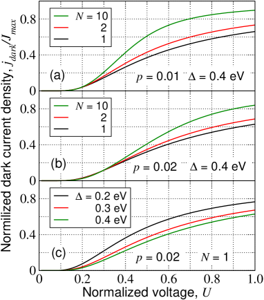
Figure 3 shows examples of the normalized dark current density versus the normalized voltage calculated using equation (11) for the GLIPs with eV and different number of the inner GLs for different parameters and . The comparison of the plots in figures 3(a) and 3(b) confirms a weak dependence of the dark current on the number of GLs and a pronounced rise of the dark current with decreasing capture efficiency (particularly at lower normalized voltages ). Higher dark currents at smaller band-offsets are naturally attributed to tunneling emission strengthening from all the GLs with decreasing of the tunneling barrier height .
As follows from equation (12) and figure 3, drastically decreases with decreasing voltage. However, at small voltages, can be so small that the tunneling exponent becomes smaller than the thermionic exponent 42 . This implies that at such voltages, the tunneling injection from the emitter GL gives way to the thermionic emission. This determines the minimal value of , at which equations (11) - (13) are still valid: . At , . This implies that the dependences shown in figure 3 are correct up to small values of (at for eV)
V Photoresponse
We limit our consideration of the GLIP operation primarily by the situations when the incident IR radiation is relatively weak.
In the case of irradiation, equations (9) and (10) should be replaced by more general equations accounting for the tunneling emission of both the thermalized and photoexcited electrons. Since the photoexcitation leads to the variations of the electric fields in the barrier layers, equation (10) in this situation should be replaced by the following equation which governs the photocurrent density :
| (17) |
where is defined by equation (4) and is governed by equation (10) leading to equation (11) and its consequences. At relatively low IR radiation intensities, such as , the electron photoexcitation can be treated as a perturbation. Considering this, into the quantities and in equation (17) on can insert the unperturbed values of the electric fields, namely, and . As a result, for the photocurrent density from equation (17) we obtain
| (18) |
Here characterizes the GLIP in dark. According to equations (8) and (9), is expressed via the dark current density and, invoking equation (12), via the voltage:
| (19) |
If or at moderated voltages , one can put in equation (18) , so that one obtains
| (20) |
The appearance of in equation (20) is associated with the contribution of the photoexcitation from the emitter GL. Since normally , for the GLIPs with not too large GLs (), equation (20) can be simplified and presented in the following form:
| (21) |
It is worth noting that the photocurrent density given by equations (18), (20), and (21) exceeds the current created by the electrons photoexcited from the emitter GL by a factor , which can be very large. This is because the photoemission from the inner GLs stimulates a strong injection of the thermalized electrons from the emitter GLs resulting in a substantial amplification of the photocurrent.
Taking into account equation (20), one can find small variations of the electric fields caused by the irradiation in all barrier layers as functions of the bias voltage and the radiation intensity . In particular, the electric field in the emitter barrier layer (as under the dark conditions). However, due to the attenuation of the IR radiation as its propagates across the GLIP structure, the electric-fields in the consequent GLs slightly increase: (such a change is proportional to the radiation intensity , which is weak in the case under consideration).
The photoexcitation leads to the variations of the electric fields in the barrier layers: an increase in and in a decrease in . At sufficiently strong irradiation, the electric field in the emitter barrier can become larger than the electric field in the bulk . In this case, the GL adjacent to the emitter GL is charged positively, and the potential profile becomes similar to that shown schematically in figure 2(b). An high radiation intensities, the electric field in the heterostructure bulk drops, so that the potential drop across the emitter layer tends to the applied voltage . This implies that tends to . Consequently, the net current density tend to a value which roughly can be estimated as . However at very high radiation intensities, the GLIP operation might, in particular, be complicated by the following effects: the saturation of the interband absorption 43 , the influence of elevated density of the photoexcited electrons on their escape 23 ; 44 , and the influence of the space-charge of the electrons propagating across the barrier layers on the electric-field distributions. These effects are beyond of our model framework.
VI Responsivity and other GLIP characteristics
The detector responsivity is usually defined as
| (22) |
Here is the device area, is the incident IR radiation power, and is the incident IR radiation flux (hence, , where is the coefficient of the IR radiation reflection from the GLIP top. Considering this and using equation (21), we arrive at the following formula for the GLIP responsivity:
| (23) |
Here , where
| (24) |
is the characteristic responsivity and the factor is determined by the conditions of reflection of the incident IR radiation from the GLIP top interface (the presence or absence of an anti-reflection coating) and its propagation across the heterostructure. The reflection from the substrate can also affect the value of . In the simplest case, the reflection factor can be expressed via : .
The deviation of the nominator in equation (23) from unity reflects the dependence of the responsivity on the emitter parameter . This deviation practically vanishes at large and . In the latter limit, the emitter can be considered as an ideal (i.e., providing the necessary injection to compensate the photoexcitation from the inner GLs 24 ; 30 ; 31 ), and the GLIP responsivity is practically independent of if the average electric field is fixed.
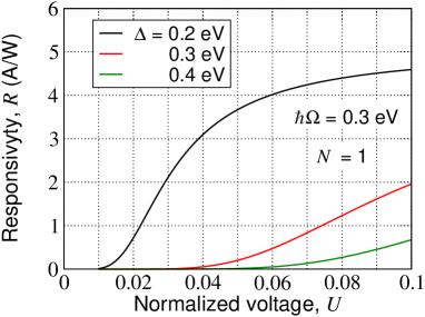
Since in GLIPs the coefficient is relatively large and the capture efficiency is relatively small ( 28 ) compered to the standard heterostructures, the characteristic responsivity can be fairly large. Indeed, setting eV and , we obtain A/W
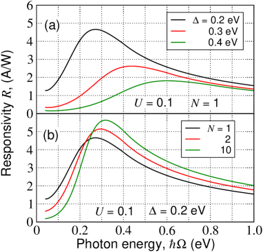
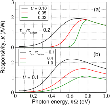
Figures 4 and 5 show the responsivity, (normalized by the reflection factor ) spectral characteristics of the GLIPs with different band offsets , number of the barrier layers , normalized voltages , capture efficiency , and . In these and the next figure it is assumed that the electron Fermi energy in the emitter GL eV. Figure 6 shows the responsivity as a function of the normalized voltage calculated for the GLIPs with different .
Among the main features of the responsivity spectral dependence, the following should be pointed out: (a) Weak dependence of the spectral characteristics on thee number of the GLs ; (b) An increase in the responsivity with decreasing capture efficiency ; (c) A marked shift of the responsivity maximum toward larger photon energies with increasing the band-offset , normalized voltage , and relative escape time ; (d) The responsivity maxima correspond to the photon energies markedly smaller than , so that the GLIPs can exhibit relatively high response at . A fairly pronounced dependence of on (i.e., the applied voltage) implies the possibility of an effective voltage control
It is important to stress that at small values of the capture parameter , the photocurrent can markedly exceed the current created solely by the electrons photoemitted from the GLs due to the effect of photoelectric gain, which implies that the electron photoemission stimulates much stronger tunneling emission from the emitter.
Taking into account that the net photoemission rate from all GLs is equal to
| (25) |
the photocurrent density (21) )can be presented as
| (26) |
where
| (27) |
is the photoelectric gain. Due to small values of in GLIPs, even at fairly large (but realistic) .
The dark current limited detector detectivity, , and its normalized version are expressed via the responsivity and the dark current density as (for example, 24 ):
| (28) |
Here for , , and one can use equations (12), (23), and (25), respectively. Considering this, we find (at )
| (29) |
Here
| (30) |
Equation (29) immediately shows that the GLIP detectivity increases with the increasing number of the inner GLs , while the responsivity (see equation (23)) is a weak funcion of . Indeed, at large , , but is virtually independent of . Some deviation from the latter is associated with the emitter effect (characterized by ). The spectral dependence of repeats that of (see figures 4 and 5).
The detectivity markedly increases with the decreasing voltage . This is owing to the pertinent drop of the dark current. However, since at small values of , the tunneling current from the emitter GL can become smaller than the thermionic current, substituting (see above) to equation (30), we obtain the following estimate for the maximum of :
| (31) |
At , the parameter can be small. In this case, equation (31) yields
| (32) |
VII Comparison with other IR photodetectors
The comparison of GLIPs and QWIPs (based, in particular, on InGaAs/AlGaAs and other heterostructures with the n-type QWs) intended for the operation in mid- and near IR ranges, shows that GLIPs can exhibit the following advantages: (i) sensitivity to normally incident radiation (no radiations coupling structures are needed; (ii) higher probability of the photo-assisted escape from the GL bound states to the continuum states above the barriers due to a relatively large universal constant . (compare with for a GaAs QW with the typical electron density cm-2 24 ); smaller capture efficiency of the electrons propagating over the barriers the into the GLs (up to the orders of magnitude - compare the data from 28 and 30 ). These advantages imply that the GLIP responsivity can exceed that of QWIPs. Since the modulation bandwidths of both GLIP and QWIPs is determined by the vertical electron transport across the barrier layers, one might assume that these bandwidths are can close to each other.
As follows from equation (21) and equation (4) from 8 , the responsivity, , of a GLIP and the responsivity, of a lateral GL-photodiode (GLPD) with a lateral p-i-n junction , are (at ) approximately equal to
| (33) |
respectively. Hence,
| (34) |
Since, the capture efficiency can be very small, the above ratio can exceed unity.
Since the electron transit time in the GLIPs (which are vertical transport devices)) can be shorter than in the GLPDs (with the lateral transport), the GLIPs can surpass the GLPDs in speed.
In the double-GL GLIPs 22 ; 23 and the UTC-PDs based on InAs/InP heterostructures 45 ; 46 , the electrons photoexcited in the emitter transfer (via the tunneling through the triangular barrier) to the undoped drift region. In contrast to the double-GL GLIPs and UTC-PDs, in which the responsivity is determined by the escape of the electrons photogenerated in the emitter layer, the GLIPs can exhibit the effect of amplification of the current produced the electrons photoexcited from the inner GLs. This effect in the GLIPs works at a weak electron capture into the inner GLs, i.e., if , but at moderate modulation frequencies. The GLIP, double-GL GLIP, and UTC-PD response at relatively high modulation frequency is affected by the electron transit across this region. One can assume that the electron transit time in UTC-PDs can be somewhat shorter than in the GLIPs because of better transport properties of the drift region materials in the former devices. However, the delay in the escape of the photoexcited electrons from the emitter limited by their diffusion (or in the best case, by the drift in the built-in electric field) across the heavily doped emitter layer, can be the main factor limiting the UTC-PD modulation bandwidths. This implies that the GLIPs (without such a delay in the emitter GL) can exhibit a high-speed performance close to that of the UTC-PDs and, hence, compete with the latter.
Similar IR photodetectors can be based on the HgCdTe heterostructures with multiple zero-gap QWs, although the specifics of these heterostructures requires a separate study.
VIII Conclusions
We proposed the GLIPs - infrared photodetectors based on vdW hetereostructures with GLs serving as the emitter, collector and absorbing layers. The GLIPs exploit the interband electron transitions between the valence band in the GLs and the continuum states in the conduction band of the barrier materials. The GLIPs should be able to operate in different ranges of the IR spectrum depending on the values of the conduction band offset between the GL and the barrier layer material. We showed that due to small capture probability of the excited electrons into the GLs together with a relatively strong interband photon absorption, the GLIPs can exhibit elevated photoelectric gain and responsivity. An increase in the number of GLs in the GLIP heterostructure can provide relatively high values of the GLIP detectivity. Among other GLIP advantages are highly conducting transparent contact GL layer, sensitivity to normally incident radiation and high speed operation. The GLIPs, which add the diversity to the IR and THz detector technology, can surpass other already realized and newly proposed photodetectors for the imaging and optical communication systems and THz photomixers.
Appendix
A1. Escape frequency and relaxation time
The tunneling rates of the thermalized and photoexcited electrons depends on the electric field, , at the GL. In equation (4) we set the escape frequency equal to and for the thermalized and photoexcited electrons respectively. Thus, it was assumed that is an exponential function of .
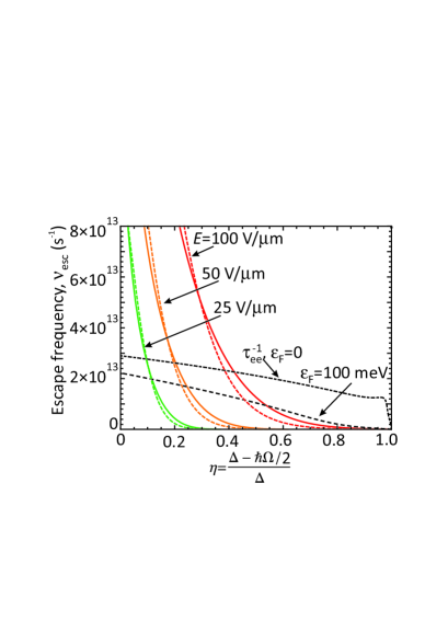
For more accurate calculations of the escape frequency as a function of the quantity we found the Schrodinger equation solutions with the complex energy for GLs embedded in a dielectric in the transverse electric field. The GL potential was modeled by a one-dimensional delta-well 26 : , where is the Dirac delta-function and is the electron wave function localization length. This quantity depends on the in-plane electron momentum due to the mismatch of dispersion laws in the GL and the barrier layer 23 ; 47 . Figure 7 shows the vs dependences calculated for different values of electric field using the above approach. The related dependences calculated using the above simplified formula are also shown by dashed lines for the material parameters corresponding to WS2 barrier layers ( eV, , and V/m).
At small the fit is not so ideal but can be considered as reasonable somewhat affecting the shape of the GLIP spectral characteristics only at .
The inverse relaxation time assumed to be primarily determined by the electron-electron scattering, so as functions of in the undoped GLs () and doped emitter GL ( meV) at and K are GLs shown in figure 7 by the dotted lines. These curves were obtained by calculating the imaginary part of the electron RPA self-energy 44 . As follows from figure 7, in the most interesting actual range of the order-of magnitude estimates yields s and . The latter characteristic times are markedly smaller that the characteristic time of the spontaneous emission of optical phonons for both the intraband and interband electron transitions. Thus, for GLIPs with WS2 barriers one can arrive at the following rough estimate: .
A2. Field-dependence of the capture efficiency
Neglecting above the local dependence of the capture parameter, we found that the electric field distribution across the device structure includes a low-field domain (in the near emitter barrier) with and a high=field domain occupying the rest of the structure (bulk) where (see equations (8) and (9). However, if depends on , the near emitter domain might be extended to a few barriers 29 .
It is worth mention that if the capture efficiency is a sufficiently strong function of , the monotonic electric-field spatial distributions can become unstable against the perturbation with the length 36 ; 37 ; 38 . Such an instability can lead to quasi-chaotic spatio-temporal electric field variations, which eventually result in the formation of stable quasi-periodic electric-field distributions 48 .
A3. Field-induced electrons in the emitter GL
The electric field in the emitter barrier induces extra electrons in the emitter GL and, hence, leads to an enhancement in the electron Fermi level or the hole Fermi level if this GL is donor or acceptor doped, respectively. As a result, the parameter can markedly depend on (decreasing with increasing ) somewhat affecting the current-voltage characteristics. Considering this effect, we find
| (35) |
. Hence
| (36) |
Setting eV and , one obtains V/m.
If , . In this case, , where
| (37) |
At eV, eV, , and one obtains .
Thus, at not too large voltages and emitter electric fields, the injection (from the contact) of the extra electrons in the emitter GL does not affect the shape of the current-voltage characteristics, but leads to a replacement of the quantity by . If the emitter barrier layer has the thickness different from , equation (6) should be modified.
A4. Carrier heating in the emitter GL
The IR irradiation can somewhat reinforce the thermionic electron emission from the emitter GL due to heating high-density 2D electron plasma in the doped emitter GL (see 21 ; 22 ; 23 ; this effect was disregarded in Section 5). The electron photoexcitation can lead to a heating of the carriers in the emitter GL slightly modifying the injection properties of the emitter. However, in the regimes considered above, the emitter properties weakly affect the GLIP characteristics, particularly, for the multiple GL devices (). This mechanism as well as the photoemission from the emitter GL can be crucial for the double-GL GLIPs without the inner GLs (i.e., with N=0) 22 ; 23 . The operation principle of the double-GL GLIPs is similar to that used in the uni-travelling-carrier photodiodes (UTC-PDs) 46 ; 47 . But such GLIPs, being potentially interesting, do not exhibit the effect of photoelectric gain, which can substantially increase the responsivity.
The bolometric mechanism associated with the electron heating due to the Drude absorption can be efficient at the relatively low radiation frequencies in the GL devices with all of the GLs doped 21 (not considered here).
A.5 Dynamic response
The evaluation of the GLIP dynamic response to transient IR radiation requires a substantial generalization of our model. It will be done elsewhere. Here we refrain to a qualitative reasoning. The dynamic operation of the GLIPs under consideration is determined by following characteristic times: the electron transit time across the GLIP , the time of the GLs charging by the injected current due to the electron capture and the time of emptying of the GLs by the electron photoexcitation from the GLs .
The transit time can be estimated as , where is the average electron velocity across the barrier layers. The latter can be set to be equal to the electron saturation velocity . The characteristic times and decrease with an increasing dc component of the incident IR radiation intensity. At small capture parameters, even at fairly strong irradiation, .
At the modulation frequencies of the incident IR radiation , the GLIP responsivity is well described by the above formulas [e.g., by equation (28)]. In this modulation frequency range, the responsivity is about and virtually independent of the number of the GLs . However, in the range , the electron capture does not manage to provide the GL recharging. As a result, the electric field and the current injected from the emitter GL do not follow the temporal variations of the IR radiation. This implies that the mechanism of the photoelectric gain is effectively switch-off. This leads to smaller values of the responsivity, which dependence on both and is rather complex. At higher modulation frequencies , the responsivity markedly drops with increasing frequency . The electron transit time limits the GLIP modulation bandwidths. Setting cm/s and nm, we obtain THz. The effect of the structural parameters on the dependences of the responsivity of single- and multiple-QWIPs on the radiation modulation frequency was studied previously 49 ; 50 . However, the results of these studies can not be directly applied to GLIPs. Recent experimental studies of the high-speed operation of the photodetectors based on double-GL vdW heterostructures with the interband photoexcitation 51 appears to be fairly promising.
IX Acknowledgments
The authors grateful to V Aleshkin , A Dubinov and A Satou for useful discussion and to N Ryabova and S Boubanga-Tombet for assistance. The work at RIEC and UoA was supported by the Japan Society for Promotion of Science (KAKENHI Grants No.23000008 and No.16H06361). V R, D S and V L acknowledge the support by the Russian Scientific Foundation (Grants No.14-29-00277 and No.16-19-10557) and the Ministry of Education and Science of the Russian Federation (Grant No.16.19.2014/K). The work at RPI was supported by the US Army Research Laboratory Cooperative Research Agreement.
References
- (1) Geim A K and Grigorieva I V 2013 Van der Waals heterostructures Nature 499 419
- (2) Mudd G W, et al. 2015 High broad-band photoresponsivity of mechanically formed InSe graphene van der Waals heterostructures Advanced Mat. 27 3760
- (3) Xia F, Wang H, Xiao Di, Dubey M, and Ramasubramaniam A 2014 Two Dimensional Material Nanophotonics Nat. Photon. 8 899
- (4) Xia, F. et al. 2009 Photocurrent imaging and efficient photon detection in a graphene transistor. Nano Lett. 9 1039
- (5) Mueller T, Xia F N A and Avouris P 2010 Graphene photodetectors for high speed optical communications Nat. Photon. 4297 301
- (6) Peters E C, Lee E J H, Burghard M and Kern, K 2010 Gate dependent photocurrents at a graphene p-n junction Appl. Phys. Lett. 97 193102
- (7) Song J C W, Rudner M S, Marcus C M and Levitov L S 2011 Hot carrier transport and photocurrent response in graphene Nano Lett. 11 4688
- (8) Ryzhii V, Ryzhii M, Mitin V and Otsuji T 2010 Terahertz and infrared photodetection using p-i-n multiple-graphene-layer structures J.Appl.Phys107 054512
- (9) Liu C H,Chang Y-C,Norris T B and Zhong Z 2014 Graphene photodetectors with ultra broadband and highresponsivity at room temperature Nat.Nanotechnol. 9273
- (10) Kim C O, Kim S, Shin D H, Kang S S, Kim J M, Jang C W, Joo S S, Lee J S, Kim J H, Choi S.-H and Hwang E 2014 High photoresponsivity in an all-graphene p-n vertical junction photodetector Nat.Commun. 5 53249
- (11) Bonaccorso F, Sun Z, Hasan T and Ferrari A C 2010 Graphene photonics and optoelectronics Nat.Photon 4 611
- (12) Ryzhii V, Ryabova N, Ryzhii M, Baryshnikov N V, Karasik V E, Mitin V and Otsuji T 2012 Terahertz and infrared photodetectors based on multiple graphene layer and nanoribbon structures Opto-Electron.Rev. 20 15
- (13) Tredicucci A and Vitielo M S 20014 Device concepts for graphene-based terahertz photonics IEEE J. Sel. Top. Quantum Electron. 20 8500109
- (14) Ryzhii V, Otsuji T, Aleshkin V Ya, Dubinov A A ,Ryzhii M, Mitin V and Shur M S, 2014 Voltage-tunable terahertz and infrared photodetectors based on double-graphene-layer structures Appl. Phys. Lett. 104 163505
- (15) Britnell L et al. 2012 Electron tunneling through ultrathin Boron Nitride crystalline barriers Nano Lett. 12 1707
- (16) Georgiou T et al 2013 Vertical field-effect transistor based on graphene-WS2 heterostructures for flexible and transparent electronics Nat. Nanotechnol. 7 100
- (17) Britnell L, Gorbachev R V, Geim A K, Ponomarenko L A, Mishchenko A, Greenaway M T, Fromhold T M, Novoselov K S and Eaves L 2013 Resonant tunneling and negative differential conductance in graphene transistors Nat. Commun. 4 1794
- (18) Feenstra R M, Jena D and Gu G 2012 Single-particle tunneling in doped graphene-insulator-graphene junctions J. Appl. Phys. 111 043711
- (19) Vasko F T 2013 Resonant and nondissipative tunneling in independently contacted graphene structures Phys. Rev.B 87 075424
- (20) Ryzhii V, Otsuji T, Ryzhii M, Aleshkin V Ya, Dubinov A A, Svintsov D, Mitin V and Shur M S 2015 Graphene vertical cascade interband terahertz and infrared photodetector 2D Materials 2 025002
- (21) Ryzhii V, Satou A, Otsuji T, Ryzhii M, Aleshkin V Ya, Dubinov A A, V. Mitin V and Shur M S 2014 Graphene vertical hot electron terahertz detectors J Appl. Phys. 116 114504
- (22) Ryzhii V, Ryzhii M, V. Mitin V, Shur M S, Satou A and T. Otsuji T 2013 Terahertz photomixing using plasma resonances in double-graphene layer structures J. Appl. Phys. 113 174505
- (23) Ma Q, Andersen T I, L. Nair N L, Gabor N M, Massicotte M, Lui C H, Young A F, Fang W, Watanabe K, Taniguchi T, Kong J, Gedik N, Koppens F H L and Jarillo-Herrero P 2016 Tuning ultrafast electron thermalization pathways in a van der Waals heterostructure Nat. Phys. 12 455
- (24) Choi K K 1997 Physics of Quantum Well Infrared Photodetectors (Singapore: World Scientific)
- (25) Lui H C and Capasso F Eds. 2000 Intersubband Transitions in Quantum Wells: Physics and Device Applications (San Diego: Academic Press)
- (26) Ryzhii V Ed. 2003 Intersubband Infrared Photodetectors (Singapore: World Scientific)
- (27) Rogalski A 2011 Recent progress in infrared detector technologies Infrared Phys. Technol. 54 136
- (28) Aleshkin V Ya, Dubinov A A, Ryzhii M and Ryzhii V 2015 Electron capture in van der Waals graphene-based heterostructures with WS2 barrier layers J. Phys. Soc. Japan 84 094703
- (29) Ryzhii V, Otsuji T, Ryzhii M, Aleshkin V Ya, Dubinov A A, V. Mitin V and Shur M S 2015 Vertical electron transport in van der Waals heterostructures with graphene layers J Appl. Phys. 117 154504
- (30) Rosencher E, Vinter B, Luc F, Thibaudeau L, Bois P and Nagle J 1994 Emission and capture of electrons in multiquantum-well structures IEEE J. Quantum Electron. 30 2975
- (31) Liu H C 1992, Photoconductive gain mechanism of quantum well intersubband infrared detectors Appl. Phys. Lett. 60 1507
- (32) Ershov M, Ryzhii V and Hamaguchi C 1995 Contact and distributed effects in quantum well infrared photodetectors, Appl. Phys. Lett. 67 3147
- (33) Thibaudeau L, Bois P and Duboz J Y 1996 A self - consistent model for quantum well infrared photodetectors J. Appl. Phys. 79 446
- (34) Ryzhii V 1997 Characteristics of quantum-well infrared photodetectors J. Appl. Phys. 81 6442
- (35) Ryzhii V and Liu H C 1999 Contact and space-charge effects in quantum-well infrared photodetectors Jpn. Appl. Phys. 38 5815
- (36) Ryzhii V, Khmyrova I, Ryzhii M, Suris R and Hamaguchi C 2000 Phenomenological theory of electric-field domains induced by infrared radiation in multiple quantum well structures Phys. Rev. B 62 7268
- (37) Ryzhii M, Ryzhii V, Suris R and Hamaguchi C 2000 Periodic electric-field domains in optically excited multiple-quantum-well structures Phys. Rev. B 61 2742
- (38) Ryzhii V and Suris R 2001 Nonlocal hot-electron transport and capture model for multiple-quantum-well structures excited by infrared radiation Jpn. J. Appl. Phys. 40 513
- (39) Gong C, Zhang H,Wang W,Colombo L,Wallace R M and Cho K 2013 Appl. Phys. Lett. 103 053513 Band alignment of two-dimensional transition metal dichalcogenides: Application in tunnel field effect transistors
- (40) Sze S M 1999 Physics of Semiconductor Devices (New York: Wiley) p 103
- (41) Gierz I, Calegari F, Aeschlimann S, Chavez Cervantes M, Cacho C, Chapman R T, Springate E, Link S, Starke U, Ast C R and Cavalleri A 2015 Tracking primary thermaliza- tion events in Graphene with photoemission at extreme time scales Phys. Rev. Lett. 115 086803
- (42) Liang S-J and Ang L K 2015, Electron thermionic emission from graphene and thermionic energy conversion Phys. Rev. Appl. 3 014002.
- (43) Vasko F T 2010 Saturation of interband absorption in graphene Phys. Rev B 82 245422.
- (44) Li Q and Das Sarma S 2013 Finite temperature inelastic mean free path and quasiparticle lifetime in graphene Phys. Rev. B 87 085406
- (45) Ishibashi T 2014 Unitraveling-carrier photodiodes for terahertz applications IEEE J. Sel. Top. 20 No6
- (46) Ishibashi T, Furuta T, Fushimi H, Kodama S, Ito H, Nagatsuma T, Shimizu N and Miyamoto Y 2000 InP/InGaAs Uni-traveling-carrier photodiodes IEICE Trans. Electron. E83 938
- (47) Dyakonov M and Shur M S 1998 Consequences of space dependence of effective mass in heterostructures J. Appl. Phys. 84 3726
- (48) Ryzhii M and Ryzhii V 2000 Nonlinear dynamics of recharging processes in multiple quantum well structures excited by infrared radiation Phys. Rev. B 62 10292
- (49) Ryzhii V, Khmyrova I and Ryzhii M 1997 High-frequency response of intersubband infrared photodetectors with a multiple quantum well structure Jpn. J. App. Phys. 36 2596
- (50) Ryzhii V 1998 High-frequency performance of single quantum well infrared photodetectors at high power densities IEEE Trans. Electron Devices 45 1797
- (51) Massicotte M, Schmidt P, Vialla F, Schadler K G, Reserbat-Plantey A, Watanabe K, Taniguchi T, Tielrooij K J and Koppens F H L 2016 Picosecond photoresponse in van der Waals heterostructures Nat. Nanotechnol. 11 42