New insights into the photochromic mechanism in oxygen-containing yttrium hydride thin films: an optical perspective
Abstract
Oxygen-containing yttrium hydride thin films exhibit a photochromic behavior: transparent thin films switch from a transparent state to a photodarkened state after being illuminated with UV or blue light. This feature has attracted much attention in recent years due to its potential applications in smart fenestration or in any device in which a response to intense light radiation is needed. However, the process responsible for the reversible change of the optical properties upon illumination is still not well understood. The objective of the present work is to shed some light on the photochromic mechanism by using an optical approach. On this basis, the optical properties of oxygen-containing yttrium hydride thin films have been studied by optical spectrophotometry and ellipsometry before (transparent state) and after UV illumination (dark state). According to the observed results, the photochromic optical change of the films can be explained quantitatively by the gradual growth, under illumination, of metallic phases within the initial wide-band gap semiconducting lattice.
.
Photochromic yttrium hydride thin films have promising technological applications in smart windows, optical switches, optical storage, sensors or in any other device in which a response to intense light radiation is required. In a window, these coatings can play an important role, both regulating the energy throughput and reducing the glare, enhancing the thermal and luminous comfort of the users YoshimuraLanghammerDam2013 ; GranqvistGreenNiklassonEtAl2010 ; BaetensJelleGustavsen2010 ; Lampert2004 .
The reversible change of the optical properties of yttrium after hydrogenation was first reported by Huiberts et al. Huiberts1996 ; in short this mechanism consists of the treatment of a metallic yttrium layer with hydrogen in order to form an yttrium hydride. As a metallic Y thin film is hydrogenated, a face centered cubic (fcc) YH2 phase is formed initially. Both Y and YH2 have a metallic-like optical behavior and therefore are opaque to visible light. However, further hydrogenation of YH2 results in the formation of hexagonal close packed (hcp) YH3, which is a wide band gap semiconducting phase, and therefore transparent in the visible spectrum. The phase transformation from fcc to hcp in YHx films is known to take place around x = 2.8 OhmuraMachidaWatanukiEtAl2007 . Besides, when the YH3 films are subjected to high pressure ( 20 GPa), a transition from the hcp YH3 phase to the fcc YH3 phase takes place, causing the gap closure of YH3 and hence a sudden drop of the optical transparency WijngaardenHuibertsNagengastEtAl2000 ; MachidaOhmuraWatanukiEtAl2006 ; PalasyukTkacz2005 ; AlmeidaKimOrtizEtAl2009 .
In addition, yttrium hydride films also exhibit photochromic (PC) behavior, i.e., the optical properties of the films change reversibly when illuminated by light of adequate energy (wavelengths in the blue or UV range). Early works by Hoekstra et al. HoekstraRoyRosenbaumEtAl2001 have shown a light induced metal insulator transition in yttrium hydrides at low temperature, and Ohmura et al. OhmuraMachidaWatanukiEtAl2007 ; OhmuraMachidaWatanukiEtAl2006 accidentally discovered PC behavior in yttrium hydride films subjected to high pressure. Later, Mongstad et al. MongstadPlatzer-BjoerkmanMaehlenEtAl2011 ; MongstadPlatzer-BjoerkmanKarazhanovEtAl2011 reported PC behavior in transparent oxygen-rich yttrium hydride films under atmospheric conditions and at room temperature. In the latter case, however, the yttrium hydride films were directly obtained by reactive magnetron sputtering rather than by the subsequent hydrogenation of a pre-deposited metallic Y layer.
The mechanism of the PC behavior in yttrium hydride is still unclear and seems to have no relation with the PC mechanism reported for transition oxides ChandranSchreudersDamEtAl2014 . In the present work, the PC behavior is studied using systematic optical measurements supported by theoretical modeling. In particular, the optical properties of oxygen-rich transparent semiconducting thin films – hereafter referred in the text simply as YHx – in both their clear and darkened state, have been investigated by ellipsometry and spectrophotometry. In addition, the optical properties of opaque metallic thin films – from now referred in the text simply as YHy, where – have been also studied. Both sets of films, YHx and YHy, were obtained by sputter deposition at a hydrogen/argon ratio 0.18 and 0.13 respectively and then exposed to air where they oxidize. The optical approach to the study of the PC mechanism is deliberate; the biggest change observed in the films under illumination takes place in the optical transmittance, while only small changes are observed in the microstructural analysis MaehlenMongstadYouEtAl2013 . The modeling of the experimental results revealed that the optical properties of the YHx (photodarkened) films can be quantitatively explained by the formation of metallic YHy domains embedded into the YHx (clear) matrix, according to the Maxwell-Garnett effective medium approximation Maxwell-Garnett1906 . The formation process of these metallic domains may consist of an insulator-to-metal transition similar to the one observed during the dehydrogenation of YH3, StepanovBourGartzEtAl2001 ; LeeKuoLinEtAl2001 according to the reversible drop of the electrical resistivity observed in the films during illumination MongstadPlatzer-BjoerkmanMaehlenEtAl2011 . Our results also support a recent work by Chandran et al. ChandranSchreudersDamEtAl2014 which reported changes of the hydrogen species in oxygen-containing yttrium hydride after illumination, suggesting the release of electrons and the formation of a metallic phase.
Figure 1 shows grazing incidence X-ray diffraction (GIXRD) patterns – obtained by using Cu-K radiation at a fixed angle of incidence of 2∘ in a Bruker Siemens D5000 diffractometer – for both transparent-semiconducting YHx [upper panel] and opaque-metallic YHy [lower panel] thin films.

The diffractogram for the YHy thin films correspond to a mix of fcc-YH2 and hexagonal-YH0.667 metallic phases, according to the standard patterns JCPDS 04-006-6935 and JCPDS 01-074-8440. The main peak, observed at around is formed by the contribution of the YH0.667 and YH2 phases in the (111) and (066) directions, respectively. Unfortunately, the analysis of the GIXRD pattern corresponding to the transparent-semiconducting YHx films deposited at higher is not straightforward. These films exhibit the characteristic features of an fcc crystalline structure that can be attributed either to an YH2 or to an YH3 (JCPDS 04-015-2399) phase. None of these two possibilities provide a satisfactory explanation to the GIXRD pattern of the YHx films; as stated before, both fcc-YH2 and fcc-YH3 phases are metallic, while the YHx films are semiconducting and transparent. In addition, the fcc-YH3 is stable only at high pressure. However, theoretical studies have demonstrated that a wide-band gap fcc phase, i.e. transparent-semiconducting, can be achieved at ambient conditions from the oxygenation of YH3 or YH2 films PishtshevKarazhanov2014 . Since yttrium hydride films deposited by sputtering and exposed to air are known to oxidize heavily (see discussion below), the diffractogram measured for the YHx films cannot be unambiguously attributed to an YH3 or YH2 stoichiometry. A complete analysis of the X-ray diffractograms for these samples can be found in the early works carried out in our laboratory MongstadPlatzer-BjoerkmanKarazhanovEtAl2011 ; MaehlenMongstadYouEtAl2013 . According to previous experiments, a lattice contraction of 0.3 - 0.4 % was observed in these YHx films upon illumination MaehlenMongstadYouEtAl2013 .
Despite this uncertainty on the stoichiometry of the YHx films, the GIXRD analysis provide two important conclusions. On the one hand, as expected, the diffractograms confirm that the samples deposited at lower contain less hydrogen, i.e. , because they exhibit an hydrogen-deficient hexagonal phase (YH0.667).
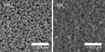
On the other hand, the lattice parameter corresponding to the fcc cubic phase matches very well the YH2 standard of 5.20 Å in the case of the YHy films, but it is much higher, about 5.40 Å, for the YHx samples. As a result, the experimental diffraction peaks for YHx in the directions (311), (220), (200) and (111) are displaced towards smaller angles compared to the standard, see Figure1 [upper pannel]. The same peaks, however, are located at the expected positions according to the standard in the YHy films, Figure 1 [lower panel]. The increase of the lattice parameter in the YHx films has been observed before and attributed to a high oxygen content in the lattice MongstadPlatzer-BjoerkmanKarazhanovEtAl2011 . Therefore and according to these observations, the oxygen content in the YHx is expected to be much higher than the one in the YHy. Indeed, an energy-dispersive X-ray spectroscopy analysis (EDS) of the equivalent samples deposited onto carbon substrates, revealed an oxygen-yttrium atomic ratio of 1.29 and 0.40 for the YHx and YHy respectively. The reason why the films deposited at lower contain less oxygen still unclear, but it can be tentatively explained by using the micrographs obtained by scanning electron microscopy (SEM) shown in Figure 2. The samples deposited at higher present a porous structure – Figure 2 [left panel] – while the films deposited at lower exhibit much more compact features – Figure 2 [right panel] –. After the deposition process, when the samples are exposed to air, the oxidation is known to take place through the pores and holes of the film StepanovBourGartzEtAl2001 . Both the micrographs and the EDS analysis were carried out in a Hitachi S-400 scanning electron microscope.
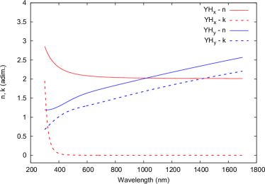
Figure 3 shows the real component, and imaginary component, of the complex refractive index for the YHx and YHy films as obtained by variable angle spectroscopic ellipsometry. The determination of for each film was achieved, as usual, by the fitting of the experimental ellipsometric angles and to a theoretical model (not shown). In this work, both modeling and data fitting were performed by using the commercial software WVASE32 from J.A. Woollam Co., Inc. This software performs an iterative fitting to the experimental data by using the Marquardt-Levenberg algorithm Kelley1999 ; Tompkins2006 . In the case of the YHx films, a simple Cauchy model Klingshirn2005 combined with an Urbach tail (exponential) provided a good fitting to the experimental measurements, while for the YHy films a Lorentz and a Tauc-Lorentz oscillators were considered Klingshirn2005 . As expected, the YHx films exhibit the typical features of a wide-band gap semiconductor sample (Figure 3), i.e., no absorption () in a wide range of wavelengths, including the visible; however, below 400 nm increases exponentially, signifying the across-the-gap optical absorption. On the other hand, varies slowly as a function of the wavelength, an usual behavior of a wide range of dielectrics and semiconductors Palik2012 . Further details on the band gap variation in these films can be found in the literature YouMongstadMaehlenEtAl2014 . As expected, the metallic YHy films exhibit high absorption in the whole region of the spectrum studied (Figure 3).
The ellipsometric measurements revealed a film thickness of 690 nm for the YHx films, which agreed very well to the result obtained by profilometry (698 nm). On the other hand, the big optical absorption in the YHy made difficult the determination of the film thickness by ellipsometry; the thickness of these samples is of about 580 nm as measured by profilometry.
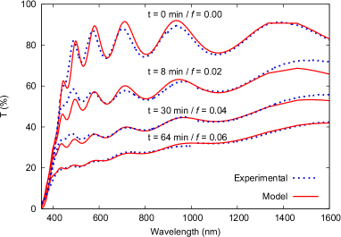
Figure 4 shows the evolution of the experimental optical transmittance (T) vs. time (t) of the YHx films under illumination (solid red lines). The samples were illuminated by a broad band light source EQ-99XFC LDLS with intense UV component, and the transmittance in the 300-1700 nm range was measured in-situ by an Ocean Optics QE65000 and a NIRQUEST512 spectrophotometers equipped with a integrating sphere. In addition, the calculated transmittance of the films – in the clear state at different stages of photodarkening – has been included in Figure 4 (dashed blue lines). The transmittance curves has been calculated by using the Fresnel equations for a thin film over a non absorbing substrate BornWolfBhatiaEtAl2000 ; BhattacharyyaGayenPaulEtAl2009 assuming: (i) the YHx (photodarkened) films consist of a composite of YHx (clear) and YHy phases, and (ii) this composite behaves optically like an homogeneous medium of effective dielectric permittivity . Assumption (ii) is valid only if the size of the YHy inhomogeneity domains are much smaller than the wavelength of the incident light Aspnes1982 ; NiklassonGranqvistHunderi1981 . On this basis, the optical constants of the photodarkened films can be approached by using Maxwell-Garnett effective medium theory, which is suitable for composites constituted by nanoparticles dispersed in a continuous matrix in the dilute limit NiklassonGranqvistHunderi1981 .
According to the Maxwell-Garnett theory, is given by Maxwell-Garnett1906 :
| (1) |
being a parameter such as:
| (2) |
where and are the respective dielectric functions of the YHx(clear) and YHy phases, is the filling factor (i.e., volume fraction) of the YHy phase and the depolarization factor. In this work the inhomogeneity domains have been considered to be spherical, therefore . On the other hand, and can be obtained from their respective experimental complex refractive index presented in Figure 3 BornWolfBhatiaEtAl2000 . As expected, the transmittance calculated for (i.e. ) matches very well the transmittance of the YHx film in the clear state ( min). Under illumination, the transparency of the films decreases gradually with time; the experimental transmittance of the YHx film after 8, 30 and 64 minutes of illumination corresponds to the one calculated for a YHx(clear)/YHy composite film with 0.02, 0.04 and 0.06 respectively (the dilute limit holds for these values of ). According to Figure 4, small inclusions of the metallic phase YHy in the YHx (clear) matrix may cause big changes in the total transmittance of the film. In fact, only a 2% in volume of the metallic YHy phase (0.02) may cause a drop of the transmittance in the visible region in more than a 30%.
The effective medium model also reproduces very well and . Figure 5 shows [panel a] and [panel b] corresponding to the photodarkened sample YHx, measured for three different angles of incidence, 50∘, 60∘ and 70∘. The experimental results corresponds to the photodarkened film (), and are depicted by means of lines with symbols, while the best fit is represented in solid red lines.
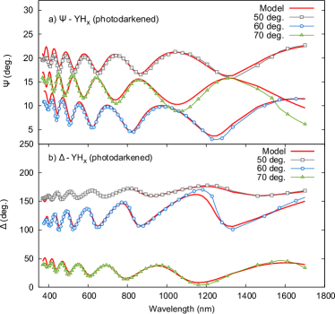
The calculated experimental ellipsometric spectra has been done assuming a thin film of optical constants described by Equation 1 and assuming .
In summary, two sets of samples, labeled as YHx and YHy, were deposited at high and low hydrogen concentrations onto glass substrates. The YHx films exhibit an fcc structure similar to the one observed in YH2 but with bigger lattice parameter Å. These films are transparent, photochromic and contain a high oxygen concentration (oxygen/yttrium ratio of 1.29). On the other hand, the YHy films were found to be opaque, exhibit a metallic behavior and are composed by YH2 and YH0.667 phases. The oxygen content in the YHy films is smaller that in the previous case (oxygen/yttrium ratio of 0.40). The dielectric permittivity in the 300 and 1700 nm wavelength range was determined by ellipsometry for both sets of samples,YHx and YHy. On the other hand, the study of the photodarkened YHx films revealed that their optical properties correspond to a composite of both phases, YHy/and YHx (clear), calculated according to Maxwell-Garnett theory. In other words, the optical properties of the photodarkened films can be explained quantitatively by the gradual formation of small metallic domains in the semiconducting matrix due to the action of energetic light. It is important to notice that the formation of a small domains of the metallic phase (with a volume fraction of 0.06 or smaller) is able to cause a substantial decrease in the optical transmittance of the films. Although these results provide valuable hints, further investigations are needed in order to reach a complete understanding of the photochromic mechanism in oxygen-containing yttrium hydride thin films.
This work has been supported by the Norwegian Research Council through the FRINATEK project 240477/F20.
References
- (1) K. Yoshimura, C. Langhammer, and B. Dam, MRS Bull. 38, 495 (2013).
- (2) C. Granqvist et al., Thin Solid Films 518, 3046 (2010).
- (3) R. Baetens, B. P. Jelle, and A. Gustavsen, Sol. Energy Mater. Sol. Cells 94, 87 (2010).
- (4) C. M. Lampert, Mater. Today 7, 28 (2004).
- (5) J. N. Huiberts et al., Nature 308 (1996).
- (6) A. Ohmura et al., Appl. Phys. Lett. 91 (2007).
- (7) R. J. Wijngaarden et al., J. Alloys Compd. 308, 44 (2000).
- (8) A. Machida et al., Solid State Commun. 138, 436 (2006).
- (9) T. Palasyuk and M. Tkacz, Solid State Communications 133, 477 (2005).
- (10) J. S. de Almeida, D. Y. Kim, C. Ortiz, M. Klintenberg, and R. Ahuja, Appl. Phys. Lett. 94 (2009).
- (11) A. F. T. Hoekstra et al., Phys. Rev. Lett. 86, 5349 (2001).
- (12) A. Ohmura et al., Phys. Rev. B 73, 104105 (2006).
- (13) T. Mongstad et al., Sol. Energy Mater. Sol. Cells 95, 3596 (2011).
- (14) T. Mongstad et al., J. Alloys Compd. 509, S812 (2011).
- (15) C. V. Chandran et al., J. Phys. Chem. C 118, 22935 (2014).
- (16) J. P. Maehlen, T. T. Mongstad, C. C. You, and S. Karazhanov, J. Alloys Compd. , S119 (2013).
- (17) J. C. Maxwell-Garnett, Philos. Tans. R. Soc. London Ser. A. 205, 237 (1906).
- (18) A. Stepanov et al., Vacuum 64, 9 (2001).
- (19) M. W. Lee, C. Y. Kuo, H. C. Lin, and H. C. Wang, J. Appl. Phys. 89, 6135 (2001).
- (20) A. Pishtshev and S. Z. Karazhanov, Solid State Commun. 194, 39 (2014).
- (21) C. Kelley, Iterative Methods for Optimization, Frontiers in Applied Mathematics, Society for Industrial and Applied Mathematics, Philadelphia (USA), 1999.
- (22) H. G. Tompkins, WVASE32® Software Training Manual, 2006.
- (23) C. F. Klingshirn, Semiconductor Optics, Springer-Verlag Berlin Heidelberg, 2005.
- (24) E. Palik, Handbook of Optical Constants of Solids, Elsevier Science, San Diego, USA., 2012.
- (25) C. C. You, T. Mongstad, J. P. Maehlen, and S. Karazhanov, Appl. Phys. Lett. 105 (2014).
- (26) M. Born et al., Principles of Optics: Electromagnetic Theory of Propagation, Interference and Diffraction of Light, Cambridge University Press, 2000.
- (27) S. Bhattacharyya, R. Gayen, R. Paul, and A. Pal, Thin Solid Films 517, 5530 (2009).
- (28) D. Aspnes, Thin Solid Films 89, 249 (1982).
- (29) G. A. Niklasson, C. G. Granqvist, and O. Hunderi, Appl. Opt. 20, 26 (1981).