Temperature-dependent photoluminescence characteristics of GeSn epitaxial layers
Abstract
epitaxial heterostructures are emerging as prominent candidates for the monolithic integration of light sources on Si substrates. Here we propose a judicious explanation for their temperature-dependent photoluminescence (PL) that is based upon the so far disregarded optical activity of dislocations. By working at the onset of plastic relaxation, which occurs whenever the epilayer releases the strain accumulated during growth on the lattice mismatched substrate, we demonstrate that dislocation nucleation can be explicitly seen in the PL data. Notably, our findings point out that a monotonous thermal PL quenching can be observed in coherent films, in spite of the indirect nature of the bandgap. Our investigation, therefore, contributes to a deeper understanding of the recombination dynamics in this intriguing group IV alloy and offers insights into crucial phenomena shaping the light emission efficiency.
The recently discovered lasing action in Wirths et al. (2015), tensile-strained Liu et al. (2010); Camacho-Aguilera et al. (2012) and nanostructured Grydlik et al. (2016) Ge has sparked the quest for identifying group IV candidates boasting a direct bandgap. Their monolithic integration on Si holds the promise to revolutionize information technology by spurring the wafer-scale establishment of advanced photonic circuits.Liang and Bowers (2010) Arguably, light-routing into the cost-effective Si platform has applications beyond communication, including biological sensing, Chow et al. (2004); Soref (2010) optical memories Ferrera et al. (2010); Ríos et al. (2015) and quantum computation.Politi et al. (2008); O’Brien et al. (2009); Shadbolt et al. (2014)
Despite the remarkable progress in heteroepitaxy and fabrication techniques that made strain and bandgap engineering readily available, the contrasting theoreticalFitzgerald et al. (1991); He and Atwater (1997); Moontragoon et al. (2007) and experimental Ryu et al. (2013); Ghetmiri et al. (2014); Gallagher et al. (2014); Wirths et al. (2015) data accumulated in the literature proved the crucial resolution of the indirect-to-direct crossover to be non-trivial and highly debated in semiconductors based on group IV materials.
The increase of the photoluminescence (PL) intensity with decreasing temperature has been recently put forward as a compelling proof that the fundamental energy gap of binary alloys can be direct in the momentum space.Wirths et al. (2015) Since this method is now increasingly applied, Stange et al. (2015); Virgilio et al. (2015); Kurdi et al. (2016); Biswas et al. (2016); Gei we find it crucial to examine the possible pitfalls associated with it. Indeed, the PL intensity is, to a good approximation, proportional to the quantum efficiency, thus prone to the entangled interplay between all the possible radiative and nonradiative processes. While the PL enhancement with decreasing temperature can be intuitively associated to direct bandgap semiconductors, which entail III-V compounds and transition metal dichalcogenide monolayers as well-cited examples, under suitable conditions it can unexpectedly occur also in indirect bandgap materialsKlein et al. (2012) including Ge.Wan et al. (2001); Kamenev et al. (2006); Lee et al. (2008); Pezzoli et al. (2014)
In this work, we demonstrate that a detailed knowledge of the recombination dynamics at ubiquitous defects, namely dislocations, is pivotal for a correct physical interpretation of the measured temperature dependence of the PL. Notably, despite the evidences that are arising for defect-related Shockley-Read-Hall recombination in group IV heterostructures,Wirths et al. (2015); Gallagher et al. (2015) yet very little is known about the nature and the optical activity of defects, chiefly dislocations. Understanding such phenomena is indeed of prime interest for overcoming the stringent roadblocks in the achievement of efficient lasing operation at room-temperature.
To tackle this challenge we focus on ultrathin epitaxial layers grown on Ge buffered Si substrates. By deliberately exploiting alloys with a Sn content below 9%, Wirths et al. (2015) we restrict ourselves to indirect gap materials and leverage their optical response as very sensitive probes of the defect-assisted recombination and generation of the photo-generated carriers. Notably, varying the epilayer thickness at a fixed Sn content provides us with samples with an adjustable strain relaxation. This eventually paves the way to suppress the plastic relaxation, selectively inhibiting dislocation nucleation. By doing so, we are well-positioned to explore how dislocations affect recombination dynamics through the opening of parasitic nonradiative recombination channels.
| Sn molar fraction (%) | thickness (nm) | Strain relaxation degree (%) |
|---|---|---|
| 5 | 70 | 0 |
| 5 | 100 | 11.5 |
| 9 | 40 | 0 |
| 9 | 70 | 0.6 |
| 9 | 80 | 6 |
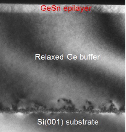
For this work the epilayers of various Ge content and thickness were grown on an 100 mm diameter Si (001) substrate via an intermediate relaxed Ge buffer layer to minimise the lattice mismatch, and consequently the compressive strain, between the epilayer and the Si substrate. The structures were grown using industrial type ASM Epsilon 2000 reduced pressure chemical vapour deposition (RP-CVD) reactor with commercially available precursors digermane () and tin-tetrachloride () diluted in Hydrogen. The epitaxial growth was carried out in Hydrogen atmosphere and at reduced pressure below 100 Torr. The Sn fractions in the epilayers and their state of strain were obtained from analysis of symmetrical (004) and asymmetrical (224) HR-XRD reciprocal space maps. The epilayers thicknesses were obtained by analysis of cross-sectional Transmission Electron Microscopy (XTEM) images. Representative XTEM data are shown in Figure 1, while the complete survey of the sample parameters is given in Table 1. It should be noted that just nm relaxed Ge buffer layer was grown on Si substrate to produce very high quality surface with RMS surface roughness below 1 nm and TDD density below for subsequent growth of epilayers. The compressive-strained (or coherent) epilayers are free from defects apart from threading dislocations arising from the Ge buffer layer. However, XTEM images of partially relaxed epilayers shows appearance of Lomer -dislocations at the /Ge interface.
To gain insight into the optical properties of epitaxial layers, PL measurements were carried out using a closed-cycle variable temperature cryostat. The samples were excited at 1.165 eV (1064 nm) by using a Nd-YVO4 laser. The optically pumped surface area had approximately a circular shape with a diameter of , which resulted in a power density of few . The PL was analyzed by a monochromator equipped with an InGaAs detector and double-checked by a Fourier transform spectrometer coupled to a PbS detector. In the former case, the PL spectra were numerically cleaned to remove the overlap with the second order peak due to the incomplete rejection of the pump.
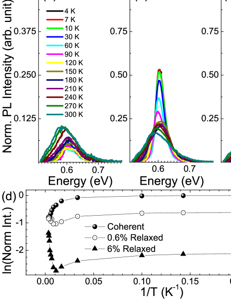
We begin by focusing on the optical properties of the samples with the highest Sn-content. Figure 2a demonstrates the temperature-dependent PL of the sample capped with the partially relaxed film. In line with recent literature works, the peak at eV is attributed to the interband optical transitions occurring in the topmost alloy layer. Notably, the PL signal turns out to be sizable up to room temperature, despite the overall reduced thickness of the /Ge stack and the complete absence of any surface passivation. At low temperature, the PL intensity increases by decreasing the relaxation degree (Figure 2a-b). Eventually, the thinnest and fully-strained counterpart demonstrates the brightest emission (Figure 2c): A result which already discloses that the attained coherent growth suppresses nonradiative bulk-like recombination pathways, whose role, in addition, can be inferred to be prominent over the competing channel offered by the surface states.
It should be noted that no PL from the underlying Ge buffer was observed at the typical emission energies of Ge-on-Si heterostructures in the range from 0.6 to 0.9 eV. Pezzoli et al. (2014) The vast majority of radiative recombination events occurring in the layer is thus likely to be due to its strong light absorption and the favorable /Ge band edge alignment alongside with the poorest optical quality of the defective Ge buffer.
By increasing the temperature, the PL features experience a well-known red-shift as a result of the bandgap shrinking, while the concomitant integrated PL intensity discloses a non-trivial temperature behavior that differs drastically for the three epilayers. Figure 2d surprisingly unveils that the coherent indirect film demonstrates the simple monotonous PL quenching commonly argued to pertain to direct bandgap materials. Furthermore, the other two partially relaxed samples exhibit a puzzling surge of the PL intensity as the lattice temperature turns higher than 90 K (). Interestingly, such a steep increase gains a larger dynamic range by increasing the strain relaxation. We emphasize that since the three epitaxial layers differ solely by the thickness, in other words by the strain, their remarkable distinction in terms of temperature characteristics under the same generation rate stems from the activated optical activity of the dislocations injected in the two thickest samples through the plastic strain relief.
The results summarized in Figure 2d for the partially relaxed samples compare well with recent reports about the optical properties of Ge/Si epitaxial architectures Pezzoli et al. (2014); Pez and prove that in Ge-rich alloys the defect-assisted recombination obeys the Schön-Klasens thermal mechanisms.Reshchikov (2014) We can therefore rationalize the physical processes leading to the results of Figure 2 by considering the following scenario. At low temperatures, carriers photogenerated in indirect bandgap alloys can be efficiently trapped at dislocations, if present, because their energy levels lie within the band gap of the host semiconductor. Above a certain critical temperature, however, the thermal activation of trapped carriers occurs, eventually strengthening the radiative interband recombination, as experimentally observed in Figure 2b for the dislocated samples.
In light of these findings, we point out that the measurement of the temperature-dependent PL characteristics as a function of the epilayer thickness, and specifically the rise of the band-edge recombination, can provide a sensitive spectroscopic method for the determination of the critical thickness above which dislocation nucleation is energetically favorable compared to the elastic energy accumulation in the growing film. This is of central importance for the ultimate fabrication of devices relying on heteroepitaxy on lattice mismatched substrates.
A closer look to the PL data of Figure 2 provides us with additional information about the recombination pathways introduced by the defects in the alloys. The negligible emission intensity at the low-energy side of the main PL peaks discloses a low quantum efficiency for the radiative recombination at dislocations. This makes the experimental investigation of the defect-assisted carrier dynamics more subtle and challenging than in Ge. This elemental semiconductor belongs to the vast class of semiconductors governed by the Schön-Klasens mechanisms,Reshchikov (2014); Pezzoli et al. (2014) where a defect-related PL peak can be often observed and its measurable temperature-dependent quenching is accompanied by a coincident rise of other PL features.Pezzoli et al. (2014) It is therefore tempting to conceive that in alloys the suppression of the dislocation-related PL might originate from the peculiar nature of the electronic states therein associated to the extended defects. Indeed our structural data are in line with the available literature reports Gallagher et al. (2015); Wirths et al. (2015) and suggest the prominence of the -dislocations, which are less common than the -dislocations typically distinguished in Ge-based heterostructures.
It is worth noticing that another consistent explanation can be put forward for the low emission efficiency of the dislocation-related PL. By alloying Ge with Sn, the offset between the direct and indirect conduction band minima decreases. The more direct-like character of the band structure of compared to the one of Ge is expected to shorten the radiative lifetime. Under this condition, the interband transitions become more probable, and consequently the radiative recombination through the band edges can increase at the expenses of the carrier recombination events, including radiative ones, taking place at the dislocation sites.
All these arguments call for dedicated and systematic investigations, presently beyond the scope of this work, aimed at the experimental determination of the minority lifetimes in the binary alloy system and at a better theoretical understanding of the so-far elusive electronic states of defects in group IV semiconductors.
In the following, we further substantiate our assertion that the measurement of the temperature-dependent PL, and thereby the recombination dynamics, is strongly affected by the presence of optically-active dislocations. To this purpose, we consider the set of indirect bandgap heterostructures having the lowest Sn content, namely 5% (see Table 1).
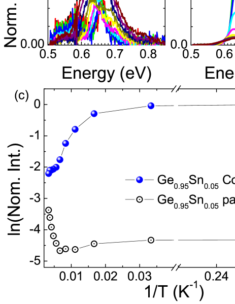
A direct comparison between Figure 2 and Figure 3 elucidates that the epilayers fully recover the optical properties previously discussed for the Sn-richer heterostructures. In particular, the temperature characteristic again demonstrates a net monotonic PL quenching as the thickness of the topmost alloy layer is reduced so that coherent growth is satisfied and plastic relaxation inhibited.
Figure 3c harbors final intriguing phenomena. The deep in the integrated PL intensity curve of the partially relaxed epilayer occurs at a temperature of about 120 K (), thus higher than what obtained for the dislocated samples. The increase of such critical temperature with decreasing the Sn content reflects the concomitant increase of the bandgap amplitude: A finding that naturally arises in the framework of rate equations modeling the capture and thermal release of carriers by the charged defect lines.Pezzoli et al. (2014); Figielski (1978)
In conclusion, by studying the temperature-dependent PL of indirect bandgap epitaxial layers in the vicinity of the plastic strain-relief, we were able to gather direct insights into the optical activity of growth defects, namely dislocations. The unveiled pivotal role of dislocations on the recombination dynamics suggests that steady-state PL measurements need to be complemented by the direct measurements of the carrier lifetime in order to precisely resolve the directness of the electronic band structure. Our experimental findings can guide and stimulate novel theoretical investigations of the electronic structures of dislocations in Ge-based heterostructures, eventually providing a deeper understanding of existing and future experiments. Finally, in view of practical applications, we anticipated an advanced contact-less spectroscopic technique to pinpoint dislocation injection in lattice mismatched heteroepitaxy.
The author thanks E. Vitiello and S. De Cesari for technical assistance, M. Guzzi and E. Grilli for fruitful discussions. This work was supported by the Fondazione Cariplo through Grant No. 2013-0623.
References
- Wirths et al. (2015) S. Wirths, R. Geiger, N. von den Driesch, G. Mussler, T. Stoica, S. Mantl, Z. Ikonic, M. Luysberg, S. Chiussi, J. M. Hartmann, H. Sigg, J. Faist, D. Buca, and D. Grützmacher, “Lasing in direct-bandgap gesn alloy grown on si,” Nature Photon. 9, 88–92 (2015).
- Liu et al. (2010) J. Liu, X. Sun, R. Camacho-Aguilera, L. C. Kimerling, and J. Michel, “Ge-on-si laser operating at room temperature,” Opt. Lett. 35, 679 (2010).
- Camacho-Aguilera et al. (2012) R. E. Camacho-Aguilera, Y. Cai, N. Patel, J. T. Bessette, M. Romagnoli, L. C. Kimerling, and J. Michel, “An electrically pumped germanium laser,” Opt. Express 20, 11316–11320 (2012).
- Grydlik et al. (2016) Martyna Grydlik, Florian Hackl, Heiko Groiss, Martin Glaser, Alma Halilovic, Thomas Fromherz, Wolfgang Jantsch, Friedrich Schäffler, and Moritz Brehm, “Lasing from glassy ge quantum dots in crystalline si,” ACS Photonics 3, 298 (2016).
- Liang and Bowers (2010) D. Liang and J. E. Bowers, “Recent progress in lasers on silicon,” Nature Photon. 4, 511 (2010).
- Chow et al. (2004) E. Chow, A. Grot, L. W. Mirkarimi, M. Sigalas, and G. Girolami, “Ultracompact biochemical sensor built with two-dimensional photonic crystal microcavity,” Opt. Lett. 29, 1093–1095 (2004).
- Soref (2010) R. Soref, “Mid-infrared photonics in silicon and germanium,” Nature Photonics 4, 495–497 (2010).
- Ferrera et al. (2010) M. Ferrera, Y. Park, L. Razzari, B. E. Little, S. T. Chu, R. Morandotti, D. J. Moss, and J. Azaña, “On-chip cmos-compatible all-optical integrator,” Nature Commun. 1, 29 (2010).
- Ríos et al. (2015) C. Ríos, M. Stegmaier, P. Hosseini, D. Wang, T. Scherer, C. D. Wright, H. Bhaskaran, and W. H. P. Pernice, “Integrated all-photonic non-volatile multi-level memory,” Nature Photon. 9, 725 (2015).
- Politi et al. (2008) A. Politi, M. J. Cryan, J. G. Rarity, S. Yu, and J. L. O’Brien, “Silica-on-silicon waveguide quantum circuits,” Science 320, 646–649 (2008).
- O’Brien et al. (2009) J. L. O’Brien, A. Furusawa, and J. Vučković, “Photonic quantum technologies,” Nature Photon. 3, 687 (2009).
- Shadbolt et al. (2014) P. Shadbolt, J. C. F. Mathews, A. Laing, and J. L. O’Brien, “Testing foundations of quantum mechanics with photons,” Nature Phys. 10, 278 (2014).
- Fitzgerald et al. (1991) E. A. Fitzgerald, P. E. Freeland, M. T. Asom, W. P. Lowe, R. A. Macharrie, B. E. Weir, A. R. Kortan, F. A. Thiel, Y. H. Xie, A. M. Sergent, S. L. Cooper, G. A. Thomas, and L. C. Kimerling, “Epitaxially stabilized gesn diamond cubic alloys,” J. Electron. Mater. 20, 489 (1991).
- He and Atwater (1997) Gang He and Harry A. Atwater, “Interband transitions in snxge1-x alloys,” Phys. Rev. Lett. 79, 1937 (1997).
- Moontragoon et al. (2007) Pairot Moontragoon, Zoran Ikonić, and Paul Harrison, “Band structure calculations of sigesn alloys: achieving direct band gap materials,” Semicond. Sci. Technol. 22, 742 (2007).
- Ryu et al. (2013) Mee-Yi Ryu, Tom R. Harris, Y. K. Yeo, R. T. Beeler, and J. Kouvetakis, “Temperature-dependent photoluminescence of ge/si and ge1-ysny/si, indicating possible indirect-to-direct bandgap transition at lower sn content,” Appl. Phys. Lett. 102, 171908 (2013).
- Ghetmiri et al. (2014) Seyed Amir Ghetmiri, Wei Du, Joe Margetis, Aboozar Mosleh, Larry Cousar, Benjamin R. Conley, Lucas Domulevicz, Amjad Nazzal, Greg Sun, Richard A. Soref, John Tolle, Baohua Li, Hameed A. Naseem, , and Shui-Qing Yu, “Direct-bandgap gesn grown on silicon with 2230nm photoluminescence,” Appl. Phys. Lett. 115, 151109 (2014).
- Gallagher et al. (2014) J. D. Gallagher, C. L. Senaratne, J. Kouvetakis, and J. Meendez, “Compositional dependence of the bowing parameter for the direct and indirect band gaps in ge1-ysny alloys,” Appl. Phys. Lett. 105, 142102 (2014).
- Stange et al. (2015) D. Stange, S. Wirths, N. von den Driesch, G. Mussler, T. Stoica, Z. Ikonic, J. M. Hartmann, S. Mantl, D. Grützmacher, and D. Buca, “Optical transitions in direct-bandgap ge1-xsnx alloys,” ACS Photonics 2, 1539–1545 (2015).
- Virgilio et al. (2015) M. Virgilio, T. Schroeder, Y. Yamamoto, and G. Capellini, “Radiative and non-radiative recombinations in tensile strained ge microstrips: Photoluminescence experiments and modeling,” J. Appl. Phys. 118, 233110 (2015).
- Kurdi et al. (2016) Moustafa El Kurdi, Mathias Prost, Abdelhamid Ghrib, Sebastienne Sauvage, Xavier Checoury, Gregoire Beaudoin, Isabelle Sagnes, Gennaro Picardi, Razvigor Ossikovski, and Philippe Boucaud, “Direct band gap germanium microdisks obtained with silicon nitride stressor layers,” ACS Photonics 3, 443–448 (2016), http://dx.doi.org/10.1021/acsphotonics.5b00632 .
- Biswas et al. (2016) S. Biswas, Jessica Doherty, Dzianis Saladukha, Quentin Ramasse, Dipanwita Majumdar, Moneesh Upmanyu, Achintya Singha, Tomasz Ochalski, Michael A. Morris, and Justin D. Holmes, “Non-equilibrium induction of tin in germanium: towards direct bandgap ge1-xsnx nanowires,” Nature Commun. 7, 11405 (2016).
- (23) R. Geiger and T. Zabel and E. Marin and A. Gassenq and J.-M. Hartmann and J. Widiez and J. Escalante and K. Guilloy and N. Pauc and D. Rouchon and G. Osvaldo Diaz and S. Tardif and F. Rieutord and I. Duchemin and Y.-M. Niquet and V. Reboud and V. Calvo and A. Chelnokov and J. Faist and H. Sigg, Germanium under high tensile stress: nonlinear dependence of direct band gap vs. strain. arXiv:1603.03454.
- Klein et al. (2012) P. B. Klein, Ugochukwu Nwagwu, J. H. Edgar, and J. A. Jr Freitas, “Photoluminescence investigation of the indirect band gap and shallow impurities in icosahedral b12as2,” J. Appl. Phys. 112, 013508 (2012).
- Wan et al. (2001) J. Wan, G. L. Jin, Z. M. Jiang, Y. H. Luo, J. L. Liu, and Kang L. Wang, “Band alignments and photon-induced carrier transfer from wetting layers to ge islands grown on si(001),” Appl. Phys. Lett. 78, 1763 (2001).
- Kamenev et al. (2006) B. V. Kamenev, E.-K. Lee, H.-Y. Chang, H. Han, H. Grebel, L. Tsybeskov, and T. I. Kamins, “Excitation-dependent photoluminescence in ge/si stranski-krastanov nanostructures,” Appl. Phys. Lett. 89, 153106 (2006).
- Lee et al. (2008) E.-K. Lee, L. Tsybeskov, and T. I. Kamins, “Photoluminescence thermal quenching in three-dimensional multilayer si/sige nanostructures,” Appl. Phys. Lett. 92, 033110 (2008).
- Pezzoli et al. (2014) F. Pezzoli, F. Isa, G. Isella, C. V. Falub, T. Kreiliger, M. Salvalaglio, R. Bergamaschini, E. Grilli, M. Guzzi, H. von Känel, and L. Miglio, “Ge crystals on si show their light,” Phys. Rev. Appl. 1, 044005 (2014).
- Gallagher et al. (2015) J. D. Gallagher, C. L. Senaratne, C. Xu, P. Sims, T. Aoki, D. J. Smith, J. Menendez, and J. Kouvetakis, “Non-radiative recombination in ge1-ysny light emitting diodes: The role of strain relaxation in tuned heterostructure designs,” J. Appl. Phys. 117, 245704 (2015).
- (30) F. Pezzoli and A. Giorgioni and K. Gallacher and F. Isa and P. Biagioni and R. W. Millar and E. Gatti and E. Grilli and E. Bonera and G. Isella and D. J. Paul and Leo Miglio, Disentangling nonradiative recombination processes in Ge micro-crystals on Si substrates, arXiv:1603.08700.
- Reshchikov (2014) Michael A. Reshchikov, “Temperature dependence of defect-related photoluminescence in iii-v and ii-vi semiconductors,” Journal of Applied Physics 115, 012010 (2014), http://dx.doi.org/10.1063/1.4838038.
- Figielski (1978) T. Figielski, “Recombination at dislocations,” Solid-State Electron. 21, 1403 (1978).