Mreferences_ABS_nourl \newcitesSreferences_ABS_nourl_suppl
Microwave spectroscopy of spinful Andreev bound states in ballistic semiconductor Josephson junctions
The superconducting proximity effect in semiconductor nanowires has recently enabled the study of new superconducting architectures, such as gate-tunable superconducting qubits and multiterminal Josephson junctions. As opposed to their metallic counterparts, the electron density in semiconductor nanosystems is tunable by external electrostatic gates providing a highly scalable and in-situ variation of the device properties. In addition, semiconductors with large -factor and spin-orbit coupling have been shown to give rise to exotic phenomena in superconductivity, such as Josephson junctions and the emergence of Majorana bound states. Here, we report microwave spectroscopy measurements that directly reveal the presence of Andreev bound states (ABS) in ballistic semiconductor channels. We show that the measured ABS spectra are the result of transport channels with gate-tunable, high transmission probabilities up to , which is required for gate-tunable Andreev qubits and beneficial for braiding schemes of Majorana states. For the first time, we detect excitations of a spin-split pair of ABS and observe symmetry-broken ABS, a direct consequence of the spin-orbit coupling in the semiconductor.
The linear conductance of a nanostructure between two bulk leads \citeMLANDAUER198191 depends on the individual channel transmission probabilities, . Embedding the same structure between two superconducting banks with a superconducting gap of gives rise to Andreev bound states (ABS) \citeMkulik1969. If the junction length is much smaller than the superconducting coherence length, , i.e. in the short junction limit, then the ABS levels depend on the phase difference between the leads according to \citeMPhysRevLett.67.3836:
| (1) |
These subgap states with are localized in the vicinity of the nanostructure and extend into the banks over a length scale determined by . Note that Eq. (1) is only valid in the absence of magnetic field, when each energy level is doubly degenerate.
Direct microwave spectroscopy has recently demonstrated the occupation of the ABS by exciting a Cooper pair in atomic junctions \citeMbretheau_nature. Unlike quasiparticle tunneling spectroscopy, which has also been used to detect ABS \citeMpillet_CNT_ABS, PhysRevLett.110.217005, resonant excitation by microwaves is a charge parity-conserving process \citeMPhysRevB.87.174521. This property enables coherent control of ABS which is required for novel qubit architectures \citeMJanvier1199 and makes microwave spectroscopy a promising tool to detect Majorana bound states \citeMPhysRevB.92.134508 in proximitized semiconductor systems \citeMPhysRevLett.105.077001, PhysRevLett.105.177002, Mourik1003.
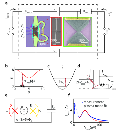
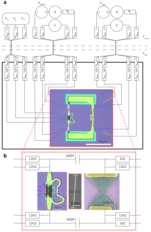
We investigate ABS excitations in Josephson junctions that consist of indium arsenide (InAs) nanowires covered by epitaxial aluminium (Al) shells \citeMCPH_InAs_nmat. The junction, where the superconducting shell is removed, is nm (device 1, see the red box in Fig. 1a) and nm long (device 2), respectively. The nanowire is then embedded in a hybrid superconducting quantum interference device (SQUID) whose second arm is a conventional Al/AlOx/Al tunnel junction (in yellow box), enabling the control of the phase drop by means of the applied magnetic flux through the SQUID loop. In the limit of a negligible loop inductance and an asymmetric SQUID, where the Josephson coupling of the nanowire is much smaller than that of the tunnel junction, the applied phase mostly drops over the nanowire link: , where is the superconducting flux quantum. We measure the microwave response \citeMbretheau_nature, PhysRevB.87.174521 of the nanowire junction utilizing the circuit depicted in Fig. 1a, where a second Al/AlOx/Al tunnel junction (in green box) is capacitively coupled to the hybrid SQUID and acts as a spectrometer. Further details on the fabrication process are given in the Supplementary Material.
In this circuit, inelastic Cooper-pair tunneling (ICPT, Fig. 1d) of the spectrometer junction is enabled by the dissipative environment and results in a DC current, \citeMPhysRevLett.73.3455:
| (2) |
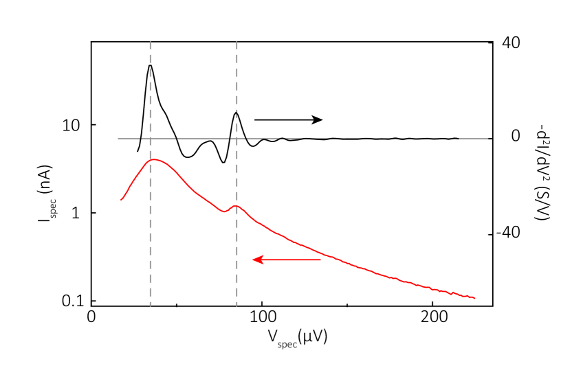
Here is the critical current of the spectrometer junction, is the applied voltage bias, and is the circuit impedance at a frequency . Since peaks at the resonant frequencies of the hybrid SQUID \citeMPhysRevLett.73.3455, bretheau_nature, so does the DC current , allowing us to measure the ABS excitation energies of the nanowire junction (Fig. 1b), as well as the plasma frequency of the SQUID (Fig. 1c).
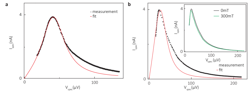
First we characterize the contribution of the plasma mode with the nanowire junction gated to full depletion, i.e. . We show the curve of the spectrometer junction of device 1 in Fig. 1f, where we find a single peak centered at eV and a quality factor . In the limit of , , where is the charging energy of the circuit and is the Josephson coupling of the tunnel junction (Fig. 1e). Estimating eV from the normal state resistance \citeMPhysRevLett.10.486, this measurement allows us to determine eV (see the Supplementary Material). The choice of a low quality factor in combination with a characteristic impedance ensures the suppression of higher order transitions and parasitic resonances.
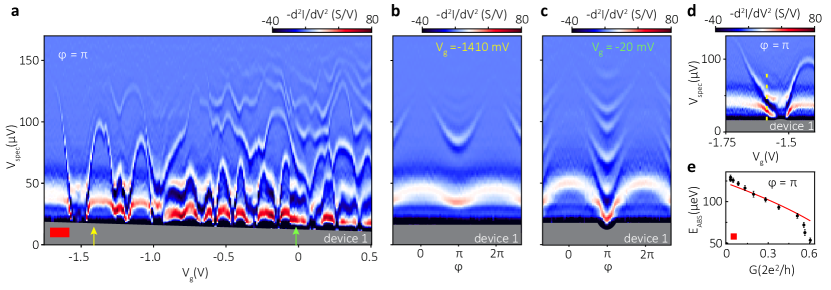
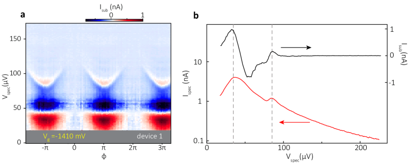
Next, we investigate the spectrometer response as a function of the gate voltage applied to the nanowire. Note that the spectrometer response to the ABS transitions is superimposed on the plasma resonance peak. In order to achieve a better visibility of the ABS lines, we display rather than (see Supplementary Material for comparison). In the presence of ABS, the spectrum exhibits peaks at frequencies where \citeMPhysRevB.87.174521. In Fig. 2a, we monitor the appearance of these peaks for an applied phase , where the ABS energy of Eq. (1) is . Notably, for values close to full depletion (see red bar in Fig. 2a), we see a gradual decrease of with increasing (black circles in Fig. 2e). In this regime, we find a good correspondence with Eq. (1), assuming single channel transport, (red solid line in Fig. 2e, see the Supplementary material on the details of the measurement of ). However, the observed eV is smaller than the eV of the thin film Al contacts, in agreement with the presence of induced superconductivity in the nanowire \citeMCPH_InAs_nnano. Increasing further, we observe a sequential appearance of peaks, which we attribute to the opening of multiple transport channels in the weak link and the consequent formation of multiple ABS \citeMPhysRevLett.67.3836 as the Fermi level, increases. We also find a strong variation of with similarly to earlier experiments \citeMDoh_2006, PhysRevLett.115.127001, PhysRevLett.115.127002. We attribute this observation to mesoscopic fluctuations in the presence of weak disorder \citeMPhysRevLett.67.3836, such that the mean free path of the charge carriers is comparable to the channel length.
Now we turn to the flux dependence of the observed spectrum, shown in Fig. 2b and 2c for two distinct gate configurations. We find a qualitative agreement with Eq. (1) with one transport channel in Fig. 2b and several channels in Fig. 2c confirming that our device is in the short junction limit. In addition, we observe the plasma mode at eV. We also find that the plasma mode oscillates with when the nanowire is gated to host open transport channels. This is expected due to the Josephson coupling of the nanowire becoming comparable to , which also causes a finite phase drop, , over the tunnel junction (see Supplementary Material). We also note the presence of additional, weakly visible lines in the spectrum which could be attributed to higher order processes \citeMbretheau_nature. However, we did not identify the nature of these excitations, and we focus on the main transitions throughout the current work.
In addition, we observe the occurrence of avoided crossings between the Andreev and plasma modes, as shown in Fig. 2d at . These avoided crossings require , which translates to a high transmission probability , and demonstrates the hybridization between the ABS excitation and the plasma mode. The coupling between these two degrees of freedom has previously been derived \citeMPhysRevB.87.174521, PhysRevB.90.134506 (see Supplementary Material), leading to a perturbative estimate for the energy splitting eV, similar to the observed value of eV. The discrepancy is fully resolved in the numerical analysis of the circuit model developed below.
We provide a unified description of the energy spectrum of the circuit as a whole, and consider the following Hamiltonian for the hybrid SQUID (Fig. 1e) \citeMPhysRevB.90.134506:
| (3) |
Here is the operator of the phase difference across the tunnel junction, conjugate to the charge operator , . The first two terms in Eq. (3) represent the charging energy of the circuit and the Josephson energy of the tunnel junction (Fig. 1e). The last term describes the quantum dynamics of a single-channel short weak link \citeMPhysRevLett.90.087003, PhysRevB.71.214505, which depends on and . For the analytic form of , see the Supplementary Material. To fully account for the coupling between the ABS excitation and the quantum dynamics of the phase across the SQUID, we numerically solve the eigenvalue problem and determine the transition frequencies with being the ground state energy.
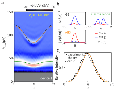
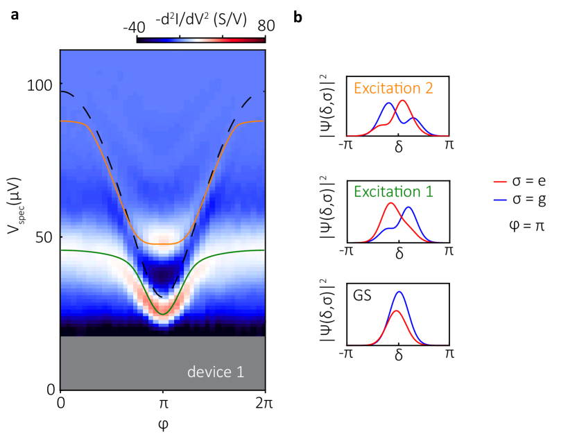
This procedure allows us to fit the experimental data, and we find a good quantitative agreement as shown in Fig. 3a for a dataset taken at mV with the fit parameters eV and . The previously identified circuit parameters and are kept fixed during the fit. We note that the observed ABS transition (orange solid line) only slightly deviates from Eq. (1) (black dashed line). The modulation of the plasma frequency (green solid line) is then defined by the model Hamiltonian with no additional fit parameters. We further confirm the nature of the plasma and ABS excitations by evaluating the probability density of the eigenfunctions of Eq. (3) at (Fig. 3b). In the ground state of (GS) and in the state corresponding to the plasma excitation (green line in Fig. 3a), the probability density is much higher in the ground state of the weak link (, blue line) than in the excited state (, red line). In contrast, the next observed transition (orange line in Fig. 3a) gives rise to a higher contribution from confirming our interpretation of the experimental data in terms of ABS excitations. Furthermore, the model can also describe measurement data with close to 1, where it accurately accounts for the avoided crossings between the ABS and plasma spectral lines (see the Supplementary Material for a dataset with ).
In Fig. 3c we show the visibility of the ABS transition as a function of the applied phase , which is proportional to the absorption rate of the weak link, predicted to be \citeMPhysRevB.87.174521. We note that in the experimental data the maximum of the intensity is slightly shifted from its expected position at . This minor deviation may stem from the uncertainty of the flux calibration. Nevertheless, using , obtained from the fit in Fig. 3a, we find a good agreement with no adjustable parameters (black dashed line). A similarly good correspondence is also found with the full numerical model (orange line) based on Eq. (3).
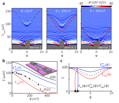
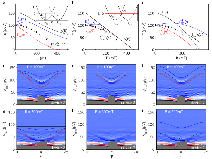
We now discuss the evolution of the ABS as a function of an in-plane magnetic field aligned parallel to the nanowire axis, which is perpendicular to the internal Rashba spin-orbit field (see the inset in Fig. 4b for measurement geometry). The applied field lifts the Kramers degeneracy of the energy spectrum, splitting each Andreev doublet into a pair . For small , the splitting is linear in , due to the Zeeman effect. However, the spin-split single particle levels are not accessible by microwave spectroscopy, which can only induce transitions to a final state with two excited quasiparticles. Thus we can only measure and expect no split of the measured spectral lines. The experimental data (Fig. 4a) shows that decreases with , while the lineshape remains qualitatively intact.
In order to explain the field dependence of , we study the behaviour of ABS in a simple model consisting of a short Josephson junction in a one-dimensional quantum wire with proximity-induced superconductivity, Rashba spin-orbit and an applied Zeeman field parallel to the wire \citeMPhysRevLett.105.077001,PhysRevLett.105.177002,PhysRevB.86.134522. Within this model, we are able to find and , and reproduce the observed quadratic decrease of the measured (black circles in Fig. 4b). Initially, as is increased, the proximity-induced gap is suppressed (black solid line), while the energy (blue solid line) increases due to the Zeeman split of the ABS. However, a crossing of the discrete ABS level with the continuum is avoided due to the presence of spin-orbit coupling, which prevents level crossings in the energy spectrum by breaking spin-rotation symmetry. The repulsion between the ABS level and the continuum causes a downward bending of , in turn causing a decrease in (black dashed line).
We perform the calculations in the limit where the Fermi level in the wire is well above the Zeeman energy and the spin-orbit energy with the effective mass and the Rashba spin-orbit coupling constant. In this case and in the short junction limit, the ratio is a function of just two dimensionless parameters: and . First we extract eV and at (leftmost panel in Fig. 4a). Then we perform a global fit on at all values and obtain a quantitative agreement with the theory for , which is in line with expected -factor values in InAs nanowires \citeMdas_2012, higginbotham_natphys_2015,albrecht_nature_2016 and . This model is consistent assuming eV at mT. Thus we attain an upper bound eV, equivalent to a Rashba parameter eVÅ in correspondence with earlier measurements on the same nanowires \citeMalbrecht_nature_2016. However, assuming the opposite limit, , the theory is not in agreement with the experimental data (see the Supplementary Material).
The theoretical energy spectrum shown in Fig. 4b predicts a ground state fermion-parity switch of the junction at a field mT, at which the lowest ABS level (red line in Fig. 4b). This parity switch inhibts the resonant excitation of the Zeeman-split ABS levels \citeMPhysRevB.77.184506 thus preventing microwave spectroscopy measurements for . This prediction is in agreement with the vanishing visibility of the ABS line at in the experiment.
In addition to the interplay of spin-orbit and Zeeman couplings, the orbital effect of the magnetic field \citeMPhysRevB.93.235434 is a second possible cause for the decrease of the ABS transition energy. Orbital depairing influences the proximity-induced pairing and results in a quadratic decrease of the induced superconducting gap: , where and is the cross-section of the nanowire. A simple model which includes both orbital and Zeeman effect, but no spin-orbit coupling, yields mT when fitted to the experimental data (see Supplementary Material for details). In this case, the fit is insensitive to the value of the -factor. However, the model also predicts the occurrence, at , of a fermion-parity switch at a field whose value depends on the -factor. Because agreement with the experimental data imposes the condition that mT, in the Supplementary Material we show that this scenario requires , which is lower than -factor values measured earlier in InAs nanowire channels \citeMdas_2012, higginbotham_natphys_2015,albrecht_nature_2016.
Furthermore, we can consider the qualitative effect of the inclusion of a weak spin-orbit coupling () in this model containing only the orbital and Zeeman effects. We note that, without spin-orbit coupling, the upper Andreev level crosses a continuum of states with opposite spin upon increasing the magnetic field (see Fig. S11c in the Supplementary Material). The crossing happens at a field of whose value depends on the -factor: using the upper bound for derived in the last paragraph, , we can estimate mT. At this magnetic field, a weak spin-orbit coupling results in an avoided crossing between the Andreev level and the continuum. As a consequence, when , the energy is bounded by the edge of the continuum and it is markedly lower than its value in the absence of spin-orbit coupling. In turn, this results in a decrease of the transition energy at , to the extent that such a model containing the joint effect of orbital depairing and weak spin-orbit coupling would depart from the experimental data in the range mT mT (see dotted line in Fig. 4b). Thus, although based on the geometry of the experiment we cannot rule out the presence of an orbital effect of the magnetic field, these considerations imply that it does not play a dominant role in the quadratic suppression of the transition energy in the present measurements.
We finally note that in all cases we neglect the effect of on the Al thin film, justified by its in-plane critical magnetic field exceeding T \citeMmeservey1971.
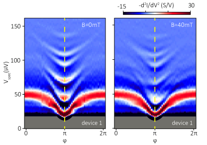
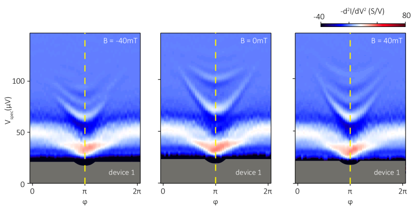
We present the ABS spectrum in the presence of several transport channels in Fig. 5. While at zero magnetic field (left panel) the data is symmetric around , in a finite magnetic field (right panel) the data exhibits an asymmetric flux dependence (see the yellow dashed line as a guide to the eye). This should be contrasted with Fig. 4a where the data for a single-channel wire are presented at different values of the magnetic field: each of the traces is symmetric around . This behavior agrees with theoretical calculations in the short-junction limit, which show that this asymmetry can arise in a Josephson junction with broken time-reversal and spin-rotation symmetries as well as more than one transport channel \citeMdoi:10.7566/JPSJ.82.054703. While the data is asymmetric with respect to , there is no visible shift of the local energy minima away from this point. This observation is consistent with the absence of an anomalous Josephson current \citeMKrive2004,PhysRevLett.101.107005,2015arXiv151201234S for our specific field configuration (magnetic field parallel to the wire), in agreement with theoretical expectations \citeMPhysRevB.82.125305,PhysRevB.93.155406,PhysRevB.92.125443.
In conclusion, we have presented microwave spectroscopy of Andreev bound states in semiconductor channels where the conductive modes are tuned by electrostatic gates and we have demonstrated the effect of Zeeman splitting and spin-orbit coupling. The microwave spectroscopy measurements shown here could provide a new tool for quantitative studies of Majorana bound states, complementing quasiparticle tunneling experiments \citeMMourik1003, das_2012. Furthermore, we have provided direct evidence for the time-reversal symmetry breaking of the Andreev bound state spectrum in a multichannel ballistic system. This result paves the way to novel Josephson circuits, where the critical current depends on the current direction, leading to supercurrent rectification effects \citeMVillegas1188, PhysRevLett.101.107001 tuned by electrostatic gates.
I Corresponding author
Correspondence and request of materials should be sent to Attila Geresdi.
II Data availability
The datasets generated and analysed during this study are available at the 4TU.ResearchData repository, DOI: 10.4121/uuid:8c4a0604-ac00-4164-a37a-dad8b9d2f580 (Ref. \citeMrawdata).
III Acknowledgements
The authors thank L. Bretheau, Ç. Ö. Girit, L. DiCarlo, M. P. Nowak and A. R. Akhmerov for fruitful discussions, and R. van Gulik, T. Kriváchy, A. Bruno, N. de Jong, J. D. Watson, M. C. Cassidy, R. N. Schouten and T. S. Jespersen for assistance with fabrication and experiments. This work has been supported by the Danish National Research Foundation, the Villum Foundation, the Dutch Organization for Fundamental Research on Matter (FOM), the Netherlands Organization for Scientific Research (NWO) by a Veni grant, Microsoft Corporation Station Q and a Synergy Grant of the European Research Council. B. v. H. was supported by ONR Grant Q00704. L. I. G. and J. I. V. acknowledge the support by NSF Grant DMR-1603243.
IV Author contributions
D. J. v. W., A. P. and D. B. performed the experiments. B. v. H., J. I. V. and L. I. G. developed the theory to analyze the data. P. K. and J. N. contributed to the nanowire growth. D. J. v. W., A. P. and D. B. fabricated the samples. L. P. K. and A. G. designed and supervised the experiments. D. J. v. W., B. v. H., L. P. K. and A. G. analyzed the data. The manuscript has been prepared with contributions from all the authors.
apsrev4-1 \bibliographyMreferences_ABS_nourl
Supplementary online material
Microwave spectroscopy of spinful Andreev bound states in ballistic semiconductor Josephson junctions
V Device fabrication
The devices are fabricated on commercially available undoped Si wafers with a nm thick thermally grown SiOx layer using positive tone electron beam lithography. First, the electrostatic gates and the lower plane of the coupling capacitors are defined and Ti/Au (nm/nm) is deposited in a high-vacuum electron-beam evaporation chamber. Next, the decoupling resistors are created using Cr/Pt (nm/nm) with a track width of nm, resulting in a characteristic resistance of m. Then, a nm thick SiNx layer is sputtered and patterned to form the insulation for the coupling capacitors and the gates. We infer fF based on the surface area of m2 and a typical dielectric constant .
In the following step, the tunnel junctions are created using the Dolan bridge technique by depositing and nm thick layers of Al with an intermediate oxidization step in-situ at mbar for 8 minutes. Then, the top plane of the coupling capacitors is defined and evaporated (Ti/Au, nm/nm) after an in-situ Ar milling step to enable metallic contact to the Al layers. Next, the InAs nanowire is deterministically deposited with a micro-manipulator on the gate pattern \citeSsuppFlohr_2011.
The channel of device 1 is defined by wet chemical etch of the aluminium shell using Transene D at C for seconds. The channel of device 2 is determined by in-situ patterning, where an adjacent nanowire casted a shadow during the epitaxial deposition of aluminium \citeSsuppKrogstrup_shadow. The superconducting layer thickness was approximately nm for both devices deposited on two facets.
Finally, the nanowire is contacted to the rest of the circuit by performing Ar plasma milling and subsequent NbTiN sputter deposition to form the loop of the hybrid SQUID. We show the design parameters of the devices in Table S1.
| Device 1 | Device 2 | |
|---|---|---|
| Channel length (nm) | 100 | 40 |
| Tunnel junction area (nm2) | ||
| Flux periodicity (T) | 38 | 120 |
| Spectrometer junction area (nm2) |
VI Measurement setup
The measurements were performed in a Leiden Cryogenics CF-1200 dry dilution refrigerator with a base temperature of mK equipped with Cu/Ni shielded twisted pair cables thermally anchored at all stages of the refrigerator to facilitate thermalization. Noise filtering is performed by a set of -LC filters (MHz) at room temperature and copper-powder filters (GHz) in combination with two-pole RC filters (kHz) at base temperature for each measurement line. The schematics of the setup is shown in Fig. S1.
VII Device circuit parameters
We characterise the circuit based on the plasma resonance observed with the semiconductor nanowire gated to zero conductance, i.e. full depletion. In this regime, we infer the environmental impedance based on Eq. (2) in the main text and assume the following form, which is valid for a parallel LCR circuit:
| (S1) |
with the dimensionless frequency. The resonance of the circuit is centered at with a quality factor of and a characteristic impedance of . Consistently with this single mode circuit, we find one peak in the trace of the spectrometer that we fit to Eq. (S1) (Fig. S2). We find a good quantitative agreement near the resonance peak, however the theoretical curve consistently deviates at higher voltages, i.e. higher frequencies. We attribute this discrepancy to additional losses or other resonant modes of the circuit not accounted for by Eq. (S1).
In addition, we use the superconducting gap and the linear resistance of the junctions to determine the Josephson energy and the Josephson inductance . With these, we infer the circuit parameters listed in Table S2.
| Device 1 | Device 2 | |
| Tunnel junction resistance (k) | 4.80 | 10.7 |
| Tunnel junction gap (eV) | 245 | 250 |
| Tunnel junction critical current (nA) | 80.2 | 36.7 |
| (eV) | 165 | 75.5 |
| Tunnel junction inductance (nH) | 4.10 | 8.94 |
| Spectrometer resistance (k) | 17.1 | 18.4 |
| Spectrometer gap (eV) | 241 | 249 |
| Spectrometer critical current (nA) | 22.2 | 21.3 |
| Shunt resistance () | 634 | 743 |
| Shunt capacitance (fF) | 12.6 | 11.1 |
| Charging energy (eV) | 25.44 | 29.1 |
| Plasma frequency (GHz) | 22.9 | 16.0 |
| Characteristic impedance () | 551 | 897 |
| Quality factor | 1.15 | 0.83 |
VIII Additional datasets
VIII.1 Spectrum analysis
Peaks in the trace of the spectrometer correspond to peaks in , i.e. allowed transitions of the environment coupled to the spectrometer. In order to remove the smooth background of the plasma mode (see Fig. S2), we evaluate , the second derivative of the to find peaks in after applying a Gaussian low pass filter with standard deviation of V. We benchmark this method in Fig. S4, and find that the peaks where correspond to the peaks in and hence is a good measure of the transitions detected by the spectrometer junction.
Alternatively, the background can be removed by linewise subtracting the detector response at \citeSsuppbretheau_nature, where the ABS does not contribute to the spectrometer response \citeSsuppPhysRevB.87.174521. We show the result of this analysis in Fig. S5. Notably, the phase dependence of the plasma mode gives rise to additional features near . Furthermore, datasets exhibiting hybridization between the ABS and plasma mode cannot be evaluated by this method. However, the line subtraction and the second derivative are in agreement if there is sufficient spacing between the plasma mode and the ABS line (see Fig. 2b and Fig. S5 for comparison).
VIII.2 I(V) trace of the hybrid SQUID
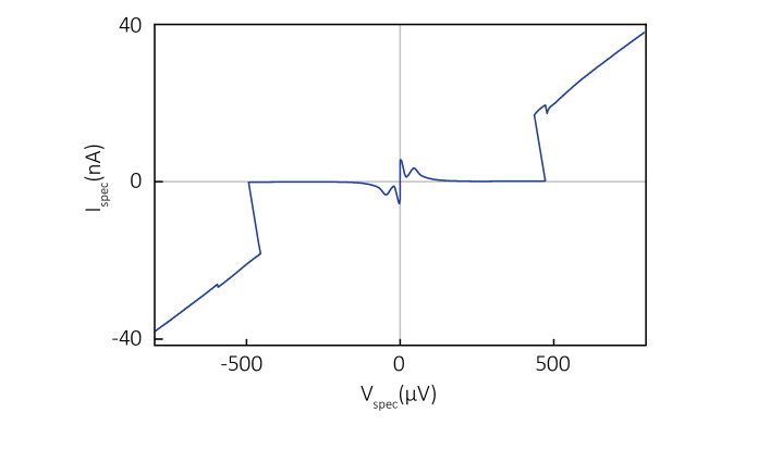
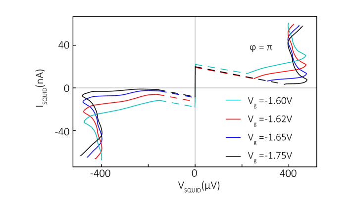
We measure the trace of the hybrid SQUID as a function of the gate voltage at (Fig. S6) and find that the subgap conductance increases with increasing gate voltage, in qualitative agreement with the contribution of multiple Andreev reflection (MAR). The zero voltage data corresponds to the supercurrent branch and the dashed lines denote the bias range where there is no data due to the bias instability of the driving circuit. In addition, we find a back-bending at the gap edge , attributed to self-heating effects in the tunnel junction.
We evaluate in Fig. 2e of the main text in the bias voltage range . We note that due to the soft superconducting gap in the nanowire junction, we did not identify MAR features after subtracting the current background of the tunnel junction.
VIII.3 Fit of ABS with high transmission
VIII.4 Time-reversal symmetry-broken ABS in bipolar magnetic field
IX Theory
IX.1 Estimate of the ABS-plasma resonance avoided crossing
Before describing the quantum model of the circuit in detail, we discuss the estimate for the energy splitting at the avoided crossing between the ABS transition and the plasma frequency shown in Fig. 2d.
For simplicity, we model the plasma oscillations as a bosonic mode with a flux-independent frequency given by , and the weak link as a two-level system, with energies defined by Eq. (1) in the main text. This system with the two independent degrees of freedom is described by the Hamiltonian . Next, we add the coupling term corresponding to the excitation of the weak link due to the voltage oscillations induced by the junction in the form
| (S2) |
where . This term describes a linear coupling between the two-level system and the phase difference across the junction. is then given by the current matrix element between the ground and excited states of the weak link, which was derived in Ref. \citeSsuppPhysRevB.87.174521:
| (S3) |
The square of this current matrix element gives the microwave absorption rate of the weak link, plotted in Fig. 3c (black dashed line) of the main text. From the coupling Hamiltonian, we immediately obtain that at , the splitting is
| (S4) |
which is the expression used for the estimate in the main text. We note that Eq. (S4) is the lowest-order estimate of the avoided crossing in the small parameter . The relatively high value of device 1 may explain the discrepancy between this simple estimate and the observed value, which is captured by the full model, see Fig. S7. Finally, we note that the expression (S3) was also derived in Ref. \citeSsuppPhysRevB.90.134506 starting from the full model (see next section). In particular, the quantity in Ref. \citeSsuppPhysRevB.90.134506 is equal to .
IX.2 Hamiltonian description of the hybrid SQUID
We now describe the theoretical model of the hybrid SQUID that was used to fit the experimental data. Our model is based on Refs. \citeSsuppPhysRevLett.90.087003 and \citeSsuppPhysRevB.71.214505. The Hamiltonian of the model is Eq. (3) of the main text, repeated here for convenience:
| (S5) |
with . The Hamiltonian of the weak link is \citeSsuppPhysRevLett.90.087003
| (S6) |
with . Here and are two Pauli matrices which act on a space formed by the ground state of the weak link and an excited state with a pair of quasiparticles in the weak link. By expanding the product above, the Hamiltonian can be put in the form . The two functions and are:
| (S7) | ||||
| (S8) |
We introduce the ground () and excited states () of the weak link in the presence of an equilibrium phase difference,
| (S9a) | ||||
| (S9b) | ||||
where is given in Eq. (1) of the main text. In the basis of eigenstates of , , they are given by
| (S10a) | ||||
| (S10b) | ||||
with the coefficients
| (S11a) | ||||||
| (S11b) | ||||||
The coefficients are normalized:
| (S12) |
To find the resonant frequencies of the hybrid SQUID, we solve the eigenvalue problem numerically. We adopt the basis for the joint eigenstates of the and operators: . For the numerical solution, we use a truncated Hilbert space where the phase interval is restricted to discrete points, with lattice spacing . A complete basis of the truncated Hilbert space is given by the vectors with (), and the eigenvector of . The Hamiltonian is thus represented as a matrix in this basis and diagonalized numerically. We choose the parameter large enough to guarantee convergence of the eigenvalues.
Once the spectrum is known, we use the transition frequencies from the ground state, , to do a least-square fit to the experimental data. The details of the numerical procedure are listed in the Jupyter notebooks available at \citeSsupprawdata.
Once an eigenstate is determined numerically, we represent its two-component wavefunction in the basis of the weak link eigenstates from Eq. (S10), evaluated at :
| (S13) |
where
| (S14) |
The probability densities plotted in Fig. 3b and Fig. S7b allow us to evaluate at a glance whether the eigenstate has a large overlap with the excited state of the (decoupled) weak link.
Finally, in Fig. 3c we show the numerical prediction for the visibility of the ABS transition as a function of the phase bias, . The visibility is determined by the absolute square of current operator matrix element between the ground state and the excited state of corresponding to the ABS transition. The current operator is \citeSsuppPhysRevB.71.214505
| (S15) |
IX.3 Equilibrium phase drop
In the main text, we have often assumed that the equilibrium phase drop across the weak link, , is close to the total applied phase, . Here, we verify this assumption by calculating the equilibrium phase drop of the hybrid SQUID model we presented in the previous section.
Since , (see Eq. (S5)), it is sufficient to show that the equilibrium phase drop across the tunnel junction is small. is given by the position where the ground state Josephson energy of Eq. (S5) is minimal for . From this condition, after taking a derivative of the Josephson energy, we obtain the following transcendental equation for :
| (S16) |
We note that the above expression defines a zero net current through the hybrid SQUID with the two arms hosting the same supercurrent. For , a good approximate solution is given by
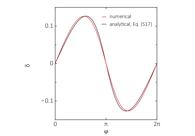
| (S17) |
up to quadratic corrections in . In Fig. S9 we show that for the parameters used in Fig. 3a, this approximate solution is very close to the exact, numerical one. Both exhibit a sinusoidal behavior with a maximum at . This confirms that the phase drop across the weak link, , remains very close to the applied phase everywhere. In particular, is exactly equal to at , where is integer.
IX.4 Andreev bound states in a proximitized Rashba nanowire in a parallel magnetic field
In this Section, we introduce the model used to describe the behavior of ABS as a function of the magnetic field . We start from the standard Bogoliubov-de Gennes (BdG) Hamiltonian of a Rashba quantum wire with proximitized -wave superconductivity and an external Zeeman field \citeSsuppPhysRevLett.105.077001,suppPhysRevLett.105.177002:
| (S18) |
Here, the two sets of Pauli matrices and act in the Nambu and spin spaces, respectively; is the effective mass in InAs \citeSsupp10.1063/1.1368156, is the Rashba spin-orbit coupling strength which defines . is the Zeeman energy, is the proximity induced gap and is the Heaviside step function. The Fermi level is measured from the middle of the Zeeman gap in the normal state band dispersion, see Fig. S11. Note that starting with Eq. (S18) we set . The superconducting phase difference between the left lead () and the right lead () is denoted by . The last term of Eq. (S18) models a short-range scatterer at , accounting for the finite channel transmission.
We seek bound state solutions of the the BdG equations,
| (S19) |
at energies . We will consider in particular two opposite regimes: (a) and (b) , see the two insets in the corresponding panels of Fig. S11. In order to find bound state solutions we proceed as follows:
-
1.
We linearize the BdG equations for the homogeneous system () around . In this way, we obtain two effective low-energy Hamiltonians, and , which are linear in the spatial derivative. They can be written as:
(S20a) (S20b) We now have three sets of Pauli matrices: (Nambu space), [distinguishing the inner/outer propagating modes, and replacing the spin matrices of Eq. (S18)], and (distinguishing left- and right-moving modes, and not to be confused with the matrices used in the previous Section). For regime (a), we have also introduced the Fermi momentum , the Fermi velocity and the energy difference between the two helical bands at the Fermi momentum. Note that, in the regime (b) where , the linearization requires , so it corresponds to the limit of strong spin-orbit coupling.
-
2.
Using Eq. (S18), we compute the transfer matrix of the junction in the normal state (), at energy . The transfer matrix gives a linear relation between the plane-wave coefficients of the general solution on the left and right hand sides of the weak link. In computing , we neglect all terms in regime (a). In regime (b), the transfer matrix is computed for , since the effect of magnetic field on scattering can be neglected to due the small dwell time in the short junction. At , the transfer matrix depends on the single real parameter , the transmission probability of the junction. The latter is given by in regime (a), and in regime (b).
-
3.
Using the transfer matrix as the boundary condition at for the linearized BdG equations, we obtain the following bound state equation for :
(S21) where is the integrated Green’s function,
(S22) and is the Fourier transform of either of the linearized Hamiltonians of Eq. (S20). [In regime (b), must be replaced by in the expression for ]. In deriving the bound state equation, we have neglected the energy dependence of the transfer matrix, which is appropriate in the short junction limit. In regime (b), this also requires that the length of the junction is shorter than , so that we can neglect resonant effects associated with normal-state quasi-bound states in the Zeeman gap, which would lead to a strong energy dependence of the transmission \citeSsuppPhysRevB.93.174502. Eq. (S21) is analogous to the bound state equation for the ABS derived in Ref. \citeSsuppPhysRevLett.67.3836, except that it is formulated in terms of the transfer matrix of the weak link, rather than its scattering matrix. Unlike its counterpart, Eq. (S21) incorporates the effect of the magnetic field in the superconducting leads. It is thus appropriate to study the effect of a magnetic field on the ABS in the limit of uniform penetration of the field in the superconductor.
-
4.
After performing the integral for , the roots of Eq. (S21) can be determined numerically. For the two regimes, this leads to the typical behavior of the ABS shown in Fig. S11 against the experimental data. As mentioned in the main text and discussed below, we find a better agreement with the experimental data for regime (a).
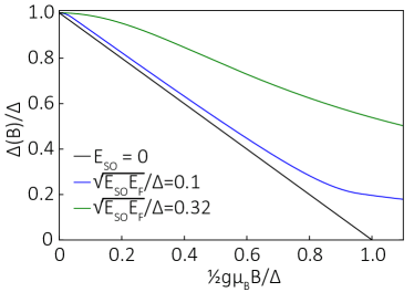
From , we can also compute the proximity-induced gap of the continuous spectrum : is the minimum value of such that the poles of touch the real axis in the complex plane [of course, can also be found by minimizing the dispersion relation obtained by diagonalizing Eq. (S20) in momentum space]. In regime (a), the relevant spectral gap is always at the finite momentum, so the behavior of depends on the strength of the spin-orbit coupling, as shown in Fig. S10. Two features are evident from the figure.
First, with increasing spin-orbit coupling, the linear behavior changes to to a quadratic suppression for small . This is due to the vanishing first-order matrix elements of the Zeeman interaction, due to the removal of the spin degeneracy of finite-momentum states by the spin-orbit interaction. Secondly, the proximity-induced gap never closes – as long as the superconductivity in the aluminium shell is present – because spin-orbit interaction competes with the Zeeman effect and prevents the complete spin polarization of the electrons. These two facts explain the behavior of shown in Fig. 4b of the main text. In regime (b) with , which is extensively discussed in the literature of Majorana bound states, due to the Zeeman-induced suppression of the gap for states at zero momentum (where spin-orbit is not effective).
An in-depth theoretical study of Eq. (S21), including a detailed analysis of its roots at finite magnetic fields and the code used in the numerical solution, is in preparation. It will also be interesting to extend the current model beyond the linearization to allow the calculation of the spectrum at arbitrary values of .
IX.5 Orbital field
Because a quadratic suppression of and the ABS energies may also be due to the orbital effect of the magnetic field, without invoking spin-orbit interaction, it is important to compare the data with this scenario. In a simple model which includes orbital and Zeeman effect, the field-dependence of the Andreev bound states may be written down as follows:
| (S23) |
Here, is the magnetic field scale which governs the suppression of the proximity-induced gap due to the orbital field, is the cross-section of the nanowire and . In writing Eq. (S23), we have neglected the effect of the orbital field on the scattering at the junction. This should be a good approximation as long as the junction is modeled by a potential with no dependence on the radial coordinate of the nanowire. Thus, essentially, the phase dependent part of the Andreev bound state energies can be obtained by replacing with in Eq. (1) of the main text. In the absence of spin-orbit coupling, the Zeeman term enters additively in Eq. (S23).
Using Eq. (S23), we can perform a fit to the experimental data to determine the optimal value mT. Note that the fit is insensitive to the value of , since drops out from the sum . However, Eq. (S23) predicts the occurrence of a fermion parity-switch at a field given by the condition . From this condition, and assuming the knowlede of both and , the -factor can then be deduced by inverting Eq. (S23) at ,
| (S24) |
The occurrence of this fermion-parity switch must be accompanied by a drastic disappearance of the ABS transition \citeSsuppPhysRevB.77.184506. In the experiment, such disappearance can be excluded up to at least mT. Therefore, by requiring that mT and using the values quoted in the main text for all other parameters, we obtain an upper bound of ,
| (S25) |
In Fig. S11c we plot the energy spectrum resulting from Eq. (S23), which includes only the orbital and Zeeman effects. The black line in Fig. S11c represents the edge of the continuous spectrum for states with spin down, . In Fig. S11c, we choose , close to the upper bound of Eq. (S25). The inclusion of a weak spin-orbit coupling in the model would not affect the curvature of and at small fields (see the blue curve in Fig. S10): the curvature would still be entirely dictated by the orbital effect. As mentioned in the main text, the Andreev level and the continuum cross at a value of the field such that . For mT and , the crossing happens at mT, see Fig. S11c. However, the inclusion of a weak spin-orbit coupling prevents the level crossing, causing the Andreev level to bend below the edge of the continuum. As a consequence, the transition energy decreases sharply at , in contrast with its behavior in the absence of spin-orbit coupling (compare the dashed and dotted lines in Fig. S11c). The behavior of in the presence of weak spin-orbit coupling clearly disagrees with the experimental data in the field range mTmT.
The considerations above motivate the approximation used in the main text, where we attribute the quadratic suppression of to the joint effect of spin-orbit and Zeeman couplings; the orbital effect does not play a dominant role in the observed dispersion.
IX.6 Fits to the data
We have presented three different scenarios that can be used to interpret the magnetic field dependence of the ABS transition energies. We have fitted all three models to the entire data set available, consisting of a flux bias sweep of the ABS spectra at six different magnetic fields ( and mT). For each flux bias at which it was visible, we have extracted the position of the ABS transition. For each value of we attributed to all the data points an error bar corresponding to the half-width at half-maximum of the ABS peak at , neglecting for simplicity the flux variation of the width. The total dataset consisted of more than 300 datapoints. We then performed a least-square fit to the ABS transition energies predicted by the three different models. The results are illustrated in Fig. S11.
apsrev4-1 \bibliographySreferences_ABS_nourl_suppl