Optical orientation of spins in GaAs:Mn/AlGaAs quantum wells via impurity-to-band excitation
Abstract
The paper reports optical orientation experiments performed in the narrow GaAs/AlGaAs quantum wells doped with Mn. We experimentally demonstrate a control over the spin polarization by means of the optical orientation via the impurity-to-band excitation and observe a sign inversion of the luminescence polarization depending on the pump power. The g-factor of a hole localized on the Mn acceptor in the quantum well was also found to be considerably modified from its bulk value due to the quantum confinement effect. This finding shows importance of the local environment on magnetic properties of the dopants in semiconductor nanostructures.
pacs:
Valid PACS appear hereI Introduction
Further miniaturization of electronic devices implies addressing as diminutive an amount of matter as possible. The ultimate goal of modern semiconductor nano-electronics is the control and read-out of single quantum states in solids Awschalom et al. (2002); Kane (1998). Optical orientation is a prospective method of addressing individual quantum sized objects. Polarized photons possess a quantized amount of spin angular momentum that transfers to charge carriers during inter-band absorption process. Promising materials for optical orientation applications are diluted magnetic semiconductors. Photo-oriented carriers interact with magnetic impurities therefore light can be used as a tool for the manipulation of spin states in semiconductors. One of the most popular magnetic dopants in II/VI and III/V materials is manganese Dietl and Ohno (2014). The outer electron shells of manganese consist of and orbitals, in such a way that two s-electrons appear in the chemical bonds. When manganese under this condition is placed in the cation sublattice it behaves as an isoelectronic impurity in II/VI semiconductors and acts as an acceptor in III/V materials. In II/VI the spin of a charge carrier interacts with a large amount of manganese spins forming a so called magnetic polaron. On the contrary in III/V the manganese spin interacts with charge carriers individually. The exchange interaction between the d-electrons and a hole with the total momentum localized on the manganese acceptor brings the neutral impurity to the ground state with full angular momentum Karlik et al. (1982) while an ionized negatively charged manganese acceptor has total spin .
It is possible to control the spin of manganese ions and other neutral acceptors in III/V based systems via optical pumping of the band-to-band transition Myers et al. (2008); Léger et al. (2006); Kudelski et al. (2007); Akimov et al. (2011). However, when the ionized impurities absorb light with the photon energy lower than the band gap Eagles (1960); Dumke (1963), another process based on the impurity-to-band transition becomes available in compensated semiconductors. It was recently proposed to use this transition as another way to achieve a spin polarization of the photoexcited electrons Kokurin et al. (2013) or as a method for read-out the Mn ion spin state Govorov (2004). In the present article we report observations of the optical orientation of charge carriers in GaAs:Mn/AlGaAs quantum wells (QW) achieved by impurity-to-band absorption.
The major advantage of using the impurity-to-band transition is a potential possibility to address the impurities individually Koenraad and Flatté (2011). Indeed, the optical orientation via a band-to-band transition Myers et al. (2008) deals with all the impurities available within the carriers diffusion length. On the contrary, the impurity-to-band transition deals only with ionized impurities that were optically addressed.
Another advantage for using the impurity related optical transitions is the absence of the Dyakonov-Perel spin relaxation mechanism D’yakonov and Perel (1971a, b). This mechanism is most responsible for the spin relaxation of delocalized charge carriers in GaAs, but it does not affect the localized impurity states. This may lead to the significantly longer spin relaxation times of photo-oriented carriers that are localized on impurities.
This article is organized as follows: the samples used in the present work are described in Sec. II. In Sec. III the results of the photoluminescence (PL) characterization are presented. There we also provide evidence that the observed PL spectra involve a recombination between an electron and the neutral Mn in the quantum well, which we denote hereafter as
The results of the PL experiments in an applied magnetic field are presented in Sec. IV. The energy position, a circular polarization of the luminescence in the magnetic field and the Zeeman splitting are discussed in detail. Section V is devoted to the optical orientation experiments carried out without magnetic field. We show that it is possible to polarize the charge carrier spins in zero magnetic field by optically pumping via the impurity-to-band transition. Finally, Sec. VI presents our conclusions.
II Samples
To address as small as possible amount of manganese spins during our optical measurements, we have grown samples with narrow quantum wells slightly doped with Mn. Each of the samples grown by molecular beam epitaxy consist of a semi-insulating GaAs -substrate overgrown with a m buffer layer and the nm GaAs single quantum well sandwiched between nm Al0.36Ga0.64As barriers. In total six samples have been grown: two undoped references and four delta-doped samples with the manganese at a flux level of cm-2. The doped samples differ in the position where Mn was introduced into the quantum well. The delta-layer was inserted either at the interfaces, both top and bottom of the well, or directly into the quantum well, at the 25% or 75% of the well width, respectively.
We obtained similar experimental results on each of the doped sample. Most of the results that we report here were obtained on the two samples that have been doped closer to the substrate.
III Photoluminescence spectra and impurity-to-band excitation
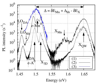
Figure 1 shows some typical PL spectra measured at 4 K and excited with the nm–line of the HeNe laser. It turns out that two distinctive types of the spectra can be detected from our samples at these conditions. Most of the sample area shows a spectrum typical for our undoped reference samples. This spectrum is made up of three main components: a transition that corresponds to recombination of the excitons localized inside the quantum well (XQW), the usual lines of the bulk exciton recombination in the GaAs buffer layer (X3D), and the radiative band of the donor-acceptor transitions in the bulk material (DA). By scanning the sample surface we have found small micron-sized spots where two additional components become visible in the PL spectrum. We assume that one of these lines is due to the quantum well excitons localized on the manganese impurities XMn and the other line corresponds to recombination of the electrons with the neutral manganeses inside the quantum well, . As it appears, the lateral distribution of Mn in our samples is strongly non-uniform.
Due to the doping non-uniformity the luminescence properties related to Mn such as its transition energy or polarization depend on the specific position of the photoexcited spot on the sample surface. However, the particular properties that we have observed do reproduce themselves uniquely well both in the Mn-poor and in the Mn-rich areas.
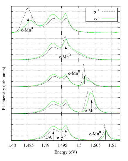
Let us first discuss the transition energy and the linewidth of the recombination. In our samples this transition appears in the range 1.48–1.51 eV. In the case of uniform doping we expect to observe a band-to-impurity recombination line at the energy lower than the band-to-band recombination and with approximately the same linewidth as XQW. We illustrated this hypothetical spectrum of the band-to-impurity transition with the band-to-band recombination line shifted by energy , the energy difference between the acceptor and the exciton related transitions in the quantum well (Fig. 1). Due to the strong doping non-uniformity and the small amount of dopants we observe not one unique broad luminescence band for transition but narrower bands randomly positioned under the envelope luminescence of the XQW downshifted in energy scale by (see Fig. 2). Figure 2 depicts the polarized PL spectra measured at different positions on the sample surface. The energy of the band-to-impurity luminescence strongly fluctuates in the range eV due to lateral variations in the quantum well width. An additional cause of the spectral irregularity is a dependence of the Mn binding energy on its exact position inside the quantum well. In such a narrow quantum well, the dopants can take only a few discrete lattice positions. A difference in the binding energy values of shallow impurities positioned in the center of a quantum well or at the interface could reach 50% Bastard (1981). Our estimates for the deep impurities in the zero–range potential approximation Demkov and Ostrovskii (1988) produce a variation of the binding energy exceeding 10%.
Controversial views about the energy of the transition have been published so far Bantien and Weber (1987); Plot et al. (1986). Some published results show that the energy difference between the exciton and the acceptor related transitions approximately equals to the binding energy of the acceptor and does not depend on the quantum well width Bantien and Weber (1987). On the other hand, manganese is considered to be a deep acceptor in GaAs, and its binding energy should not be strongly affected by the quantum confinement. Then the energy difference between the exciton– and the acceptor–related transitions is given by Plot et al. (1986), where is the acceptor binding energy, is the quantum confinement of the heavy–hole subband, is the exciton binding energy. It should be pointed out that the observed energy difference strongly decreases with an increasing acceptor concentration inside the quantum wells Holtz et al. (1998). Because in this paper we are dealing with the samples of low manganese concentration, the observed transition energy includes the hole confinement shift, in agreement with results published in Plot et al. (1986). We obtain meV using a numerical solution for the well width nm with the barriers height 200 meV, and the heavy hole mass in the well and in the barriers. The exciton binding energy is taken as meV Mathieu et al. (1992). We use the manganese binding energy meV, which is increased from its bulk value meV due to the effect of quantum confinement Romanov and Averkiev (2012).
Dopants in semiconductors are always partly ionized due to technologically unavoidable small amount of doping compensation. In our samples the degree of manganese ionization is enhanced because the quantum well is subjected to electric fields of the surface depletion layer. This makes it possible to optically pump the photoluminescence using an impurity related absorption. In such case an ionized manganese acceptor captures the pump photon of energy less than the band gap in the quantum well. That produces a photoexcited electron in the quantum well and the neutral acceptor.
To optically pump the samples, our setup is equipped with two lasers. A HeNe laser pumps the quantum well related luminescence and we employ a Ti-sapphire laser tuned to 1.53 eV in order to pump the impurity-to-band transition. In a two-color experiment the both lasers are focused on the same PL spot. In our measurements under the Ti-sapphire laser excitation, the line appears only at the spots where both XMn and transitions can be detected under the HeNe excitation first. This observation is the direct evidence that here we deal with the impurity-to-band excitation inside the GaAs/AlGaAs quantum well doped with partially compensated impurities.
IV Polarized photoluminescence in magnetic field and Zeeman splitting
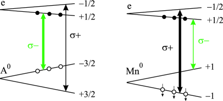
The photoluminescence of recombination in GaAs has an opposite sign of the circular polarization in comparison with a shallow acceptor in the magnetic field Karlik et al. (1982). This is caused by the exchange interaction between the localized hole and and the core electrons of Mn. The Hamiltonian of a manganese acceptor in the applied magnetic field , including the exchange interaction, is given by
| (1) |
Here is the exchange parameter, and are the spin of the d-electrons and the hole angular momentum, respectively, with and the corresponding g-factors, and is the Bohr magneton.
It is easy to find all 12 possible optical transition probabilities using the selection rules in dipole approximation and taking into account the angular momentum coupling in the ground state (see table 1).
| , | +5/2 | +3/2 | +1/2 | -1/2 | -3/2 | -5/2 |
|---|---|---|---|---|---|---|
| +1 | 0 | 0 | ||||
| 0 | 0 | 0 | ||||
| -1 | 0 | 0 |
In the narrow quantum wells, the quantum-confined splitting between the acceptor states and can be comparable in value with the exchange parameter , where is about meV Nestoklon et al. (2015). For a shallow acceptor in 3.7-nm thick quantum well parameter is about meV Masselink et al. (1985), and for a deep center this value can be further reduced. Thus, we are likely to find ourselves in the intermediate situation, when . In order to describe the quantum–well confinement we use an extra term in the Hamiltonian:
| (2) |
Note, that in the 2D-case, when , the ground–state wavefunctions are composed of components exclusively. In the 3D–limit, when , the wavefunctions remain dominated by the same heavy-hole components as before, although the ground state includes an admixture of the light holes Averkiev et al. (1988). However, there will be no qualitative difference in the main character of the ground states in these two limiting cases. In the 2D-description, which we use from now on, there are only two possible optical transitions given by:
| (3) |
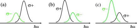
The left panel in Fig. 3 sketches the optical transitions of a conduction electron to a common shallow acceptor. In the applied magnetic field the ground state is populated with a hole. The component in this case dominates in the circular polarized photoluminescence. As shown in Fig. 4 (c) the dominating line is also shifted to the lower energies. This scheme is in full agreement with our measurements as well as with the results published before Bimberg (1978). The Zeeman splitting for the shallow acceptor in our measurements (Fig. 5) produces , assuming the electron g-factor bulk value of .
The right panel in Fig. 3 presents the optical transitions involving Mn. Here the situation is more complex due to the Zeeman splitting of the final state after recombination. The initial state of Mn is () as discussed before. In this case the -polarized transition dominates in the Mn-related photoluminescence, see Eq.(3). This analysis is supported by the experimental results firstly published in Karlik et al. (1982)
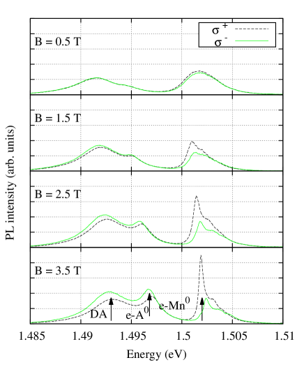
In Fig. 2 we have shown the polarized PL spectra measured at different spots of the doped samples. The well-resolved and transitions at 1.492 eV and 1.497 eV clearly show a negative sign of the polarization. As discussed above, the energy of transition varies across the sample. However, in all PL spectra the transition has a positive sign of the polarization, independent on the spot where the photoluminescence is collected. This observation supports our assignment of the transitions to the Mn inside quantum well.
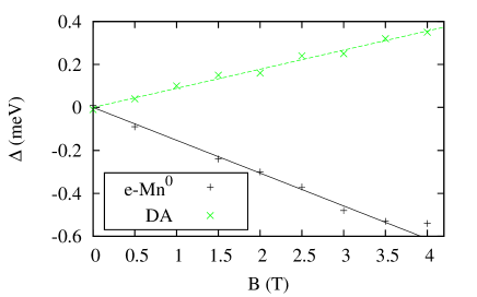
Now let us discuss the Zeeman splitting of the transition. Here we assume that the Zeeman splitting is much less than both the exchange and the quantum-confined splittings. In bulk GaAs the complexity of this transition is due to splitting of the final state. This splitting does not affect the PL polarization degree but it has to be accounted in the spectral position of the polarized components. Here we neglect the splitting in the conduction band because the g-factor of electrons is small in comparison with the g-factor of holes in such quantum wells Hannak et al. (1995). Then we can express the splitting of the transition as . Using and from the ESR measurements Schneider et al. (1987) we get a positive splitting and the dominating component at a higher energy than the component as shown in Fig. 4 (a). That kind of splitting was experimentally observed in bulk GaAs:Mn Kikkawa et al. (1994). Our experiments also produce the dominating component but at the lower energy as illustrated in Fig. 4 (b). For the reference, we also depict in the same figure (see Fig. 4 (c)) a shallow acceptor in the bulk GaAs with a sign assignment of the splitting from Bimberg (1978).
The most probable reason for the observed sign of Zeeman splitting is a reduction of the hole g-factor due to the effect of strong quantum confinement. The g-factor of the core d-electrons is independent on material parameters because of their atomic-scale confinement. On the contrary, the hole g-factor, in addition to a paramagnetic contribution described by the Luttinger material parameter (see, for instance Luttinger (1956)), has also an orbital contribution Bir et al. (1967). And the quantum confinement considerably changes the hole g-factor Wimbauer et al. (1994); van Bree et al. (2012). A hole bound by an acceptor already displays a renormalized g-factor even in the bulk semiconductor Gelmont and Dyakonov (1973). A g-factor of the acceptor-bound hole in the quantum well has substantially different value (possibly even an opposite sign) depending on a ratio between the Bohr radius and the quantum well width. Numerous earlier experiments demonstrated that the hole g-factor is strongly modified by the size and geometrical anisotropy of the nanostructure, and also depends on a given position of the impurity atom inside the nanostructure van Bree et al. (2012); Snelling et al. (1992); Krebs et al. (2009); Kudelski et al. (2007).
In bulk GaAs the Mn g-factor in the ground state can be expressed as with Averkiev et al. (1988). In narrow quantum wells the energy structure of Mn undergoes a change and, in the 2D limit, can be described with only two states and corresponding to as already expressed in Eq. (3) with the g-factor . Hence in the 2D-model the spectral splitting in magnetic field depends on the hole g-factor only, as the Zeeman splitting of the d-shell electrons in initial and final states cancels out. By taking into account the experimentally measured value of splitting presented in Fig. 5 and Fig. 6, we obtain in the 2D limit . The actual values of the Mn hole g-factor vary in the range at different positions on the sample (Fig. 2). Such a strong variation of the g-factor is caused by fluctuations in the quantum well width and by different actual positions of the impurity inside the quantum well. This result is in a good agreement with recent measurements of the Mn–related PL in InAs quantum dots Krebs and Lemaître (2013) where authors also observed strong fluctuations in the Mn-related g-factor.
To conclude this section, we would also briefly mention that our 2D-model produces the value of of about that is renormalized from the bulk value of by the quantum confinement, while the 3D-limit would result in a value down to .
V Optical orientation in zero magnetic field
Despite the fact that the optical orientation in semiconductors is a well-studied phenomenon Meier and Zakharchenya (1984), so far as we know, nobody used the impurity-to-band transition to optically orient the charge carriers spins. We carry out our experiments in a traditional optical orientation framework exciting impurity-to-band transition with a circularly polarized light and detecting the polarized photoluminescence. Our results on the optical orientation measurements significantly vary from point to point on the sample similarly to the above described magneto-luminescence experiments. Here we describe the three most representative properties of the measured spectra: 1) a higher-energy broadening of the spectra at high pump power, 2) the spectral dependence of polarization and 3) the dependence of polarized photoluminescence intensity on the pump density. Our aim is to show that all these properties can be described within one consistent model.
Let us consider a limited amount of partly compensated manganese acceptors inside the quantum well. A binding energy of the acceptor is fluctuating due to a randomized distance between that acceptor and the barriers. Acceptor states at the lower energies remain always neutral while the acceptors at the higher energies are ionized due to the doping compensation. We shall refer to these neutral acceptors as equilibrium Mn0. Under intensive photoexcitation via the impurity-to-band transition, the ionized acceptors should also become neutral. In the same way, we shall refer to these acceptors as non-equilibrium Mn0 acceptor states.
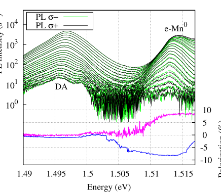
Figure 7 shows the polarized PL spectra taken at different pump power in zero magnetic field while the pump photon energy was set to eV. We observe a strong high-energy broadening of the line while the DA line spectral position and its spectral shape is not changed. This high-energy broadening is caused by the photo-induced neutralization of the high-energy acceptor states leading to a production of the non-equilibrium Mn0.

The intensity of transition versus pump power (Fig. 8) shows a dependence characteristic for the impurity–related luminescence. It is linear in limit of the low pump power and saturates at the higher pump power. We fit this experimentally observed dependence by a two-parameter function:
| (4) |
where is the pump power, is a value of the saturated intensity, and is a parameter that is set equal to a slope of the experimentally observed dependence at zero pump power. The fitting function is easily derived for the case of nearly total doping compensation from the following rate equation:
| (5) |
here is a concentration of the photo-excited electrons, and and are the concentrations of ionized and neutral Mn acceptors, respectively; is the ionized impurity absorption coefficient and is the coefficient of bimolecular recombination; is the photoexcitation volume, which is equal to a product of the laser spot area and the width of the quantum well, cm3. To solve Eq. (5), one has to include charge conservation and , where is the total concentration of the Mn dopants.
It follows then that the concentration can be estimated as:
| (6) |
Substituting cm-1, and cms-1 in Eq. (6) with experimental values s-1 and cm2 taken in units of the pump light flux, we estimate the total Mn concentration as cm-3 that corresponds to the surface density of about cm-2 or to a few hundred Mn atoms within the excitation area in a diffraction limit.
The polarization degree and the photoluminescence intensity saturates as the pump power is increased. The value of maximum polarization at the saturation point fluctuates from spot to spot in the range 5–15 % for the pump photon energy eV. It becomes higher if the transition energy is closer to the pump energy, which is a typical behavior for the optical orientation. In the majority of the studied spots the polarization of photoluminescence has a distinctive spectral dependence (Fig. 9). Under the -pump the electron-to-manganese PL is mostly -polarized at the high-energy side of spectrum while the polarization is close to zero at the low-energy side. We suppose that the specific polarization of manganese acceptors affects the polarized spectra: the non-equilibrium high-energy acceptor states are polarized via impurity-to-band transition while the equilibrium acceptors keep zero net-polarization.
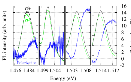
Fig. 10 depicts the dependence of PL polarization degree vs pump power. Here we observe an intriguing phenomenon: the sign of polarization is changed from negative to positive while pump power increases (Fig. 7). It is a quite rarely observed phenomenon and its description has to employ a complicated scheme of spin and energy relaxation processes Shabaev et al. (2009). Here we propose an approximate description of the polarization sign inversion in our experiments based on the suggested model of the impurity-to-band transition.
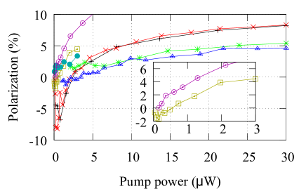
The positive polarization, as we observe in the limit of high pump power, corresponds to an ordinary optical spin orientation of the photoexcited electrons. In this regime, the spin relaxation time can be estimated from the degree of polarization. Indeed, the lifetime of the bimolecular recombination equals and from Eq. (5) one can easily derive
| (7) |
where we introduced characteristic pump power . In the limit of high pump power (), when the transition is saturated, the radiative lifetime becomes constant . In other words, in this limit there are many photo-charge carriers generated within the photo absorption (photo-neutralization) cross section of , that is . In our case this leads to an estimate of ns, the value that is in a good agreement with the radiative lifetimes in compensated GaAs:Mn reported elsewhere Astakhov et al. (2008). The corresponding electron spin relaxation time can be then estimated from the experimental polarization values following the dependence of the polarization degree on the ratio between and Meier and Zakharchenya (1984):
| (8) |
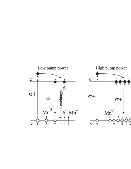
The maximum polarization value of can only be achieved in the 2D-case if . Then the photo-excited electrons keep their spins oriented until they recombine, with the PL polarization positive due to the selection rules (Fig. 11, right panel). In our case, the transition displays polarization of 5–15% that translates into ns, a typical value for this material. We note that for the optically saturated transition the magnetic nature of impurity does not play any role in the optical orientation of the spins. Identical behavior would be equally observed in the case of a non-magnetic dopant.
This is different from when the transition is not saturated, in the limit of low pump power , and here we infer that the negative polarization is due to the net spin polarization of the ionized . Indeed, in this regime the radiative recombination slows down as decreases and the radiative times become dependent on itself: . In our experiments this regime is realized at of a few tenth of W. From Eq. (7), this pump power corresponds to a microsecond range of the bimolecular recombination. That closely matches the spin relaxation time reported for the manganese ions in GaAs Akimov et al. (2011). In this limit the optical spin orientation of the photoexcited electrons does not contribute to the PL polarization as now. It is now the d-electrons of ionized manganese Mn- that become optically oriented (Fig. 11, left panel). In accordance with Eq. (3), only with absorbs the photons. Then the photo-excited acceptors and electrons lose their spin shortly after the photoexcitation. Once they recombine, an equal amount of with and gets back into the system, that is to say that the ions with are accumulated. Despite the fact that the photo-excited electrons become spin-polarized via the exchange interaction with the neighboring in the predominant state. This provides a negative sign of the polarization according to Eq. (3).
The optical orientation measurements carried out at the different pump wavelengths (see inset of Fig. 10) support our description. Under the pump with higher photon energy the electron polarization becomes lower due to stronger spin relaxation of photo-excited electrons. In that case the PL polarization is determined by polarization of Mn- ions and gets the negative sign at low pump power. Under the pump with lower photon energy the photo-excited electrons conserve its spins and PL polarization is positive.
VI Conclusion
We carried out magneto-optical and optical orientation experiments using the impurity-to-band excitation in Mn doped narrow quantum wells. The g-factor of hole localized on the Mn acceptor was found to be modified due to the quantum confinement effect from its bulk value to . We have shown that it is possible to optically polarize the charge carriers by means of impurity-to-band excitation. We also observe a sign inversion in the circular polarization of the Mn-related luminescence and suggest a model based on the impurity-to-band excitation to explain this experimental observation by optical orientation of the Mn ions.
Acknowledgements.
We acknowledge funding from Russian Science Foundation. P.V.P., N.S.A., P.M.K. and A.Yu.S. were supported by project 14-42-00015 (experiments and general discussion). I.A.K. and Yu.L.I. were supported by project 14-12-00255 (theory).References
- Awschalom et al. (2002) D. D. Awschalom, D. Loss, and N. Samarth, eds., Semiconductor spintronics and quantum computation (Springer, Berlin, 2002).
- Kane (1998) B. E. Kane, Nature 393, 133 (1998).
- Dietl and Ohno (2014) T. Dietl and H. Ohno, Rev. Mod. Phys. 86, 187 (2014).
- Karlik et al. (1982) I. Ya. Karlik, I. A. Merkulov, D. N. Mirlin, L. P. Nikitin, V. I. Perel, and V. F. Sapega, Fiz. Tverd. Tela 24, 3550 (1982), [Sov. Phys. Solid State, 24, 2022, (1982)].
- Myers et al. (2008) R. C. Myers, M. H. Mikkelsen, J. M. Tang, A. C. Gossard, M. E. Flatte, and D. D. Awschalom, Nat. Mater. 7, 203 (2008).
- Léger et al. (2006) Y. Léger, L. Besombes, J. Fernández-Rossier, L. Maingault, and H. Mariette, Phys. Rev. Lett. 97, 107401 (2006).
- Kudelski et al. (2007) A. Kudelski, A. Lemaître, A. Miard, P. Voisin, T. C. M. Graham, R. J. Warburton, and O. Krebs, Phys. Rev. Lett. 99, 247209 (2007).
- Akimov et al. (2011) I. A. Akimov, R. I. Dzhioev, V. L. Korenev, Yu. G. Kusrayev, V. F. Sapega, D. R. Yakovlev, and M. Bayer, Phys. Rev. Lett. 106, 147402 (2011).
- Eagles (1960) D. Eagles, J. Phys. Chem. Solids 16, 76 (1960).
- Dumke (1963) W. P. Dumke, Phys. Rev. 132, 1998 (1963).
- Kokurin et al. (2013) I. A. Kokurin, P. V. Petrov, and N. S. Averkiev, Fiz. Tekh. Poluprovodn. 47, 1244 (2013), [Semiconductors 47, 1232 (2013)].
- Govorov (2004) A. O. Govorov, Phys. Rev. B 70, 035321 (2004).
- Koenraad and Flatté (2011) P. M. Koenraad and M. E. Flatté, Nat. Mater. 10, 91 (2011).
- D’yakonov and Perel (1971a) M. I. D’yakonov and V. I. Perel, Zh. Eksp. Teor. Fiz. 60, 1954 (1971a), [Sov. Phys. JETP 33, 1053 (1971)].
- D’yakonov and Perel (1971b) M. I. D’yakonov and V. I. Perel, Fiz. Tverd. Tela 13, 3581 (1971b), [Sov. Phys. Solid State 13, 3023 (1972)].
- Bastard (1981) G. Bastard, Phys. Rev. B 24, 4714 (1981).
- Demkov and Ostrovskii (1988) Yu. N. Demkov and V. N. Ostrovskii, Zero-range potentials and their applications in atomic physics (Plenum, New York, 1988).
- Bantien and Weber (1987) F. Bantien and J. Weber, Solid State Commun. 61, 423 (1987).
- Plot et al. (1986) B. Plot, B. Deveaud, B. Lambert, A. Chomette, and A. Regreny, Journal of Physics C: Solid State Physics 19, 4279 (1986).
- Holtz et al. (1998) P. O. Holtz, A. C. Ferreira, B. E. Sernelius, A. Buyanov, B. Monemar, O. Mauritz, U. Ekenberg, M. Sundaram, K. Campman, J. L. Merz, and A. C. Gossard, Phys. Rev. B 58, 4624 (1998).
- Mathieu et al. (1992) H. Mathieu, P. Lefebvre, and P. Christol, Phys. Rev. B 46, 4092 (1992).
- Romanov and Averkiev (2012) K. S. Romanov and N. S. Averkiev, Fiz. Tekh. Poluprovodn. 46, 805 (2012), [Semiconductors 46, 786 (2012)].
- Nestoklon et al. (2015) M. O. Nestoklon, O. Krebs, R. Benchamekh, and P. Voisin, Semicond. Sci. Technol. 30, 035019 (2015).
- Masselink et al. (1985) W. T. Masselink, Y.-C. Chang, and H. Morkoç, Phys. Rev. B 32, 5190 (1985).
- Averkiev et al. (1988) N. S. Averkiev, A. A. Gutkin, E. B. Osipov, and M. A. Reshchikov, Fiz. Tverd. Tela 30, 765 (1988), [Sov. Phys. Solid State 30, 438 (1988)].
- Bimberg (1978) D. Bimberg, Phys. Rev. B 18, 1794 (1978).
- Hannak et al. (1995) R. Hannak, M. Oestreich, A. Heberle, W. Rühle, and K. Köhler, Solid State Commun. 93, 313 (1995).
- Schneider et al. (1987) J. Schneider, U. Kaufmann, W. Wilkening, M. Baeumler, and F. Köhl, Phys. Rev. Lett. 59, 240 (1987).
- Kikkawa et al. (1994) J. M. Kikkawa, J. J. Baumberg, D. D. Awschalom, D. Leonard, and P. M. Petroff, Phys. Rev. B 50, 2003 (1994).
- Luttinger (1956) J. M. Luttinger, Phys. Rev. 102, 1030 (1956).
- Bir et al. (1967) G. L. Bir, E. I. Butikov, and G. E. Pikus, Fiz. Tverd. Tela 9, 1068 (1967), [Sov. Phys. Solid State 9, 835 (1967)].
- Wimbauer et al. (1994) Th. Wimbauer, K. Oettinger, Al. L. Efros, B. K. Meyer, and H. Brugger, Phys. Rev. B 50, 8889 (1994).
- van Bree et al. (2012) J. van Bree, A. Yu. Silov, P. M. Koenraad, M. E. Flatté, and C. E. Pryor, Phys. Rev. B 85, 165323 (2012).
- Gelmont and Dyakonov (1973) B. L. Gelmont and M. I. Dyakonov, Fiz. Tekh. Poluprovodn. 7, 2013 (1973), [Sov. Phys. Semicond. 7, 1345 (1974)].
- Snelling et al. (1992) M. J. Snelling, E. Blackwood, C. J. McDonagh, R. T. Harley, and C. T. B. Foxon, Phys. Rev. B 45, 3922 (1992).
- Krebs et al. (2009) O. Krebs, E. Benjamin, and A. Lemaître, Phys. Rev. B 80, 165315 (2009).
- Krebs and Lemaître (2013) O. Krebs and A. Lemaître, Phys. Rev. Lett. 111, 187401 (2013).
- Meier and Zakharchenya (1984) F. Meier and B. Zakharchenya, eds., Optical Orientation (Elsevier, Amsterdam, 1984).
- Shabaev et al. (2009) A. Shabaev, E. A. Stinaff, A. S. Bracker, D. Gammon, A. L. Efros, V. L. Korenev, and I. Merkulov, Phys. Rev. B 79, 035322 (2009).
- Astakhov et al. (2008) G. V. Astakhov, R. I. Dzhioev, K. V. Kavokin, V. L. Korenev, M. V. Lazarev, M. N. Tkachuk, Yu. G. Kusrayev, T. Kiessling, W. Ossau, and L. W. Molenkamp, Phys. Rev. Lett. 101, 076602 (2008).