Spin-polarized quasiparticle tunneling in spin-filter pseudospin-valve devices
Abstract
Spin selective nature of spin-filter tunnel junctions can be integrated with conventional metallic ferromagnets to regulate spin polarized quasiparticles in superconducting devices. We report fabrication of pseudo spin-valve device made with a bilayer of nitride spin-filter tunnel barrier (DyN or GdN) and a transition metal ferromagnet (Co and Gd). We show resistance switching in these devices corresponding to parallel and antiparallel configuration of their mutual magnetization direction. With optimal deposition process partial nitridation of the Co layer can be achieved. The magnetically dead native CoNx layer at the Co-DyN interface acts the role of the barrier in these devices. In pseudo spin-valve with Co, lower resistance was found for antiparallel state compared to parallel configuration. Reverse resistance switching behavior was observed for the pseudo spin-valves with Gd. Presence of resistance switching in these devices further confirm the spin-filtering nature of DyN and GdN tunnel barrier. Quasiparticle transport at different temperatures in these devices was found to be compatible with conventional N-I-S tunnelling model. These devices can be further engineered to regulate spin polarized supercurrent in superconducting spintronics devices.
pacs:
85.30.Mn, 75.76.+j,74.70.Ad,74.50.+r,72.25.Dc,I Introduction
Superconducting spintronics depends on the creation and manipulation of spin polarized current in devices involving superconducting (S) and ferromagnetic (F) materialsLinder ; Blamire ; Wakamura . In particular, Josephson junction of the S-F-S type have got a lot of attention recently due to their potential application in quantum computing and spintronics Makhlin ; Clarke ; Yamashita . The spin singlet Cooper pair amplitude undergoes an oscillatory decay inside a ferromagnetic metal. This oscillatory behavior can lead to a phase difference of between the two superconductors depending on the thickness of the ferromagnet in the S-F-S junctionBuzdin ; Ryazanov ; Kontos . The possibility of junction was initially proposed by Bulaevskii et. al. for a Josephson junction including magnetic impurities in the tunnel barrierbulaevskii . A lot of experimental and theoretical investigation has been done on Josephson junctions since thenBell ; jason-prl ; Sellier ; Halterman . In the case of tunnel junctions the transition from 0 to -state can be distinguished in the differential conductance spectra in the quasiparticle tunnelling regime. In Al-Al2O3-PdNi-Nb tunnel junctions when thickness of the ferromagnetic layer is increased features in the superconducting density of state (DOS) are reversed with respect to the normal state indicating a 0 to state transitionKontos . More complicated tunnel junctions of the from SFIFSkrivoruchko ; bergeret , SIFISPetkovic , SIFSwides ; larkin ; Wild and SIsFSbakurskiy ; Bakurskiy-prb ; vernik ; ryazanov has also been proposed theoretically and observed experimentally. However, compared to metallic S-F-S Josephson junction tunnelling devices have been relatively poorly explored experimentally sofar. It has been theoretically predicted that it is possible to generate spin-triplet superconducting correlations in a ferromagnet with magnetic inhomogeneity in contact with a superconductorbergeret ; eschrig . The triplet correlations decay over much longer length scale than usual. Some experimental evidences has also been reported for their existencesosnin ; robinson-science ; khaire ; keizer ; anwar ; jwang . However, a democratic experimental evidence of long-range odd-frequency spin-triplet pairs is still missing. As tunnelling process is more spin selective than the diffusive counter part, spin-valves involving tunnel barriers can provide more definitive evidence for spin-triplet pairs
Recently, we have shown that magnetic semiconductors like GdN, DyN, etc., are quite compatible with superconducting NbN and are very promising materials for superconducting spintronicsmuduli ; muduli-arxive ; pal ; blamire ; senapati . We have shown that spin polarized tunnel current can be very effectively generated due to spin filtering through these tunnel barriers. With unique properties of spin-filter tunnel junctions it is possible to create composite structures in combination with ferromagnets to design new kind of superconduting spintronics devicesNagahama ; baek ; leclair ; moodera-rev ; shiro ; Giazotto ; Kawabata . However, integrating normal ferromagnets within all nitride device is not trivial and possible nitridation of the metal layers and nature of interfaces have to be carefully considered. In this paper, we report fabrication and electrical characterization of psuedospin-valve devices made of a strong ferromagnet and a spin-filter tunnel barrier. We have used GdN and DyN tunnel barrier as spin polarizer and Co and Gd as analyzer. A comparison of resistance switching behaviour has been done between Co-DyN and Gd-GdN type devices. Devices with different thickness of DyN were fabricated to optimize tunnelling regime. The tunneling nature of the device has been analyzed through current-voltage (I-V) measurements at different temperatures. Quasiparticle transport through the psuedospin-valve devices has been compared to N-I-S tunnelling model. We show spin regulation can be achieved in these devices by controlling relative magnetization of the two magnetic layers. We provide a qualitatively explanation for the resistance switching behavior observed in our psuedo spin-valve device.
II Experimental
Multilayer structures NbN-FM-FI-NbN were fabricated by DC sputtering in an ultrahigh vacuum (UHV) chamber at room temperature (here FM = Co, Gd and FI= DyN, GdN). Nitride layers were deposited by sputtering of high purity metal targets in an Ar/N2 gas mixture with deposition condition as described in the referencemuduli ; muduli-arxive . The Co layer was deposited at 1.5 Pa in a pure Ar gas with 40 W sputtering power. Ferromagnetic Gd was also deposited in a similar condition with lower 20 W sputtering power. Thickness of different layers were controlled by regulating the speed of a rotating substrate stage. The multilayer structure NbN-FM-FI-NbN was deposited in the order from left to right insitu without breaking vacuum. The nitridation of Co and Gd during subsequent deposition of DyN or GdN strongly depends on time they are exposed to the nitride plasma. Therefore, thickness of the DyN or GdN layer plays a crucial role in controlling the interfacial nitridation. In thicker films the Co (Gd) layer is exposed to nitride plasma for a longer time which can lead to higher nitridation. The CoNx thin film is known to be magnetic with a perpendicular magnetic anisotropyMatsuoka . However, a very thin layer of CoNx might be magnetically dead and prevent magnetic coupling between the FI and FM. In the case of multilayer with Gd, nitrogen deficient GdNx might be formed at the interface. The thickness of the top and bottom NbN was kept fixed at 50 nm in all the multilayers. While thickness of the Co and DyN layer was varied in the series. As the top and bottom NbN is common in all the devices, we have used abbreviation FM( nm)-FI( nm) throughout this paper to represent different kind of devices. Here and represent thickness of the ferromagnetic metal and insulator in nanometer, respectively. Devices were fabricated using photolithography in a mesa structure. The junction dimension was defined by etching the top NbN in CF4 plasma for 30 sec and milling 10 min with Ar-ion after that. Top contact was made with Nb electrode after SiO2 lift-off. Lateral dimension of the junctions were 7 m 7 m. Schematic of the mesa device is shown in the inset of Fig. 1. Differential conductance () was measured with a lock-in technique in a custom made dip-stick using liquid helium. Spin valve measurements were done in a closed-cycle helium refrigerator from Cryogenics Lmt. The measurements were done in a four-probe configuration with DC bias current. The magnetization of the multilayer films deposited at the same time were carried out with a SQUID magnetometer. In this paper measurements done on one representative sample is shown. The reproducibility and behaviour of other devices are shown in the supplementary material.
III Results and Discussion
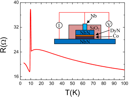
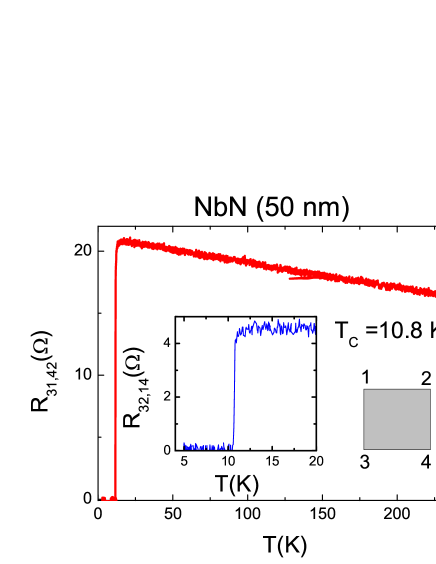
Figure 1 shows temperature dependence of resistance of a Co(5 nm)-DyN(2.5 nm) device measured with a bias current I = 100 A. The resistance showed semiconducting temperature dependence with a small deviation below 20 K. Similar was also found for Co-GdN devices (see supplementary figure SFig. 2). The temperature dependence of resistance in these devices is most likely determined by the most resistive part i.e., Co-DyN interface, where formation of disordered CoNx is possible. See supplementary material (SFig. 3) for of devices with different thickness of Co and DyN. Superconducting transition of NbN in the Co(5 nm)-DyN(2.5 nm) device can be seen at = 10.6 K as a sharp drop in the resistance. The superconducting coherence length of NbN in the dirty limit can be determined from the expression; . Using diffusion constant = 1.48 10-4m2s-1 and =10.6 K we found = 4.1 nm (See Supplementary Information for calculation of diffusion constant) kartikapl . The superconducting coherence length inside Co can be calculated from the expression; ; where and are the diffusion constant and the Curie temperature of Co, respectively. With = 6 10-4m2s-1 and = 1388 K, we found =1.8 nm jwang . The thickness of the Co in all our Co-DyN devices is 5 nm which is larger than both and . For conventional spin-singlet case the superconducting correlations decay over a length in the diffusive ferromagnet. Therefore, our NbN-FM-FI-NbN devices can be considered as N-I-S type device instead of a S-N-I-S type device.
III.1 Tunneling behavior
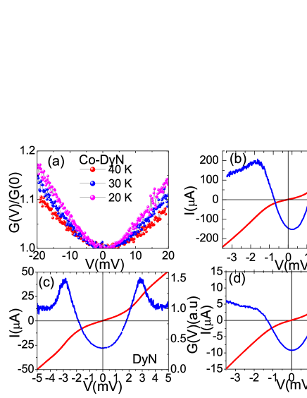
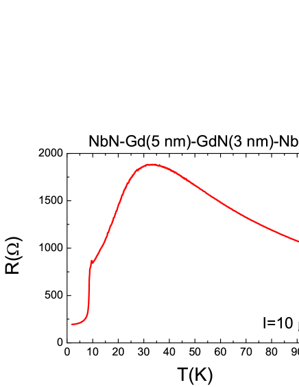
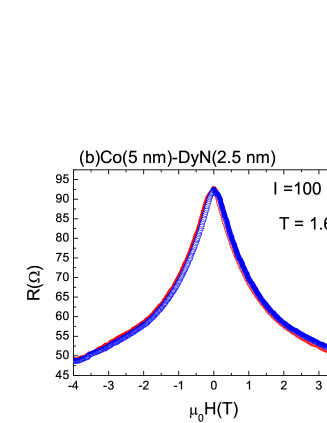
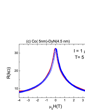
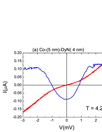
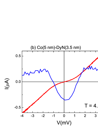
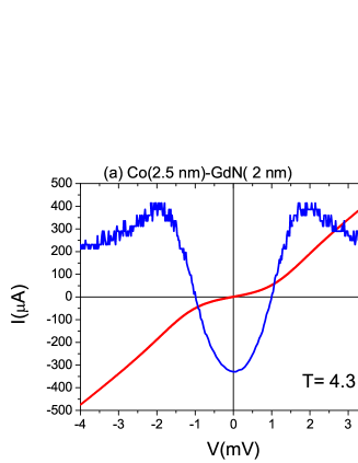
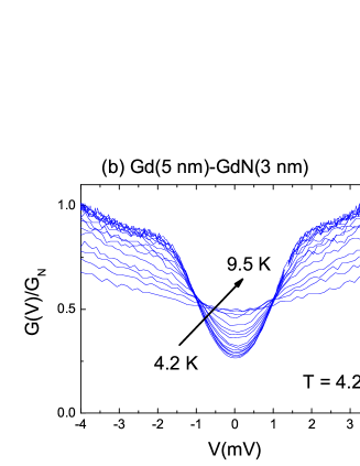
Current-voltage (I-V) measurements were done at different temperatures to understand the nature of the electrical transport in the devices. Figure 2(a) shows the conductance normalized to its value at for the Co(5 nm)-DyN (2.5 nm) device. Clear parabolic conductance spectra at 20, 30 and 40 K suggest tunnelling-type transport in this devices through all temperature range. The spectra of the devices were also measured at different temperatures below the of NbN. The I-V and normalized conductance spectra of the same junction measured at 4.2 K is shown in Fig. 2(b). Fully developed superconducting gap structure with 2 2.94 meV can be seen. For comparison Fig. 2(c) shows I-V and normalized conductance spectra of a NbN-DyN-NbN tunnel junction without Co. A superconducting gap 4 5.68 meV can be observed in this device. Figure 2(d) shows I-V and normalized conductance spectra of a Gd(5 nm)-GdN(3 nm) device. The Superconducting gap was found to be 2 3.18 meV in this case. In the Gd(5 nm)-GdN(3 nm) device the actual thickness of GdN can be slightly larger than the deposited value due to partial nitridation of Gd during deposition. As 4 nm GdN is at the limit of tunnelling to diffusive transport, the gap edges are slightly smeared in the Gd(5 nm)-GdN(3 nm) device. We have previously observed that the superconducting gap structure disappers in the conductance spectra for junctions with DyN thickness 4 nm muduli . In the Co-DyN devices well defined gap structure was absent for DyN thickness 4 nm (see supplementary figure SFig. 8 for conductance spectra of Co-DyN devices with different thickness of DyN). The superconducting gap value found from the conductance spectra for our S-FN-FI-S device is slightly greater than the value found for S-FI-S type devices. Therefore, the Co-DyN and Gd-GdN devices are not truly N-I-S type device as expected.
To further confirm this the spectra below the of NbN in our devices can be compared with NIS-type tunnel model. Normalized tunneling conductance of a NIS junction at a bias voltage can be written as:
| (1) |
where is Fermi-Dirac distribution function and is the normalized BCS density of state of the superconductor. Here is the normal state conductance of the junction. Following Dynes approachdynes the quasiparticle density of states can be written as, . Here the smearing parameter is included to consider finite lifetime of quasiparticles. Quasiparticles have finite lifetime at non zero temperature due to presence of some energy levels within the superconducting gap. Besides, impurities and pinholes in the tunnel barrier has also shown to contribute to kalpwik ; Schrieffer . In our case magnetism of the tunnel barrier (FI) and normal electrode (FN) might further add to .
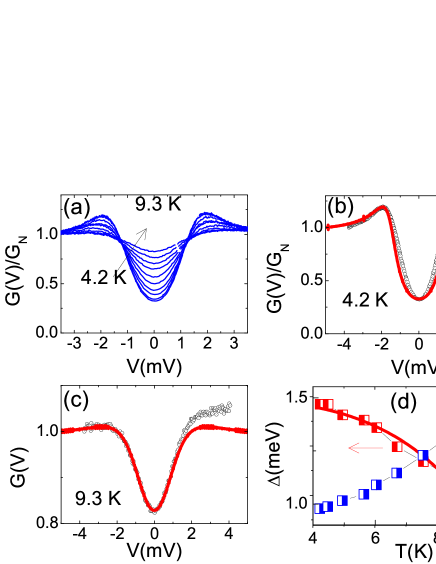
Figure 3(a) shows the temperature evolution of conductance spectra of the Co(5 nm)-DyN(2.5 nm) device measured in the range 4.2 to 9.3 K. Fitting of the Eq. (1) (red solid line) to the conductance spectra measured at 4.2 and 9.3 K is shown in Fig. 3(b) and (c), respectively. We found acceptable fit of the conductance spectra to the NIS-tunneling model at all temperatures by adjusting smearing parameter . Fig. 3(d) shows plot of extracted fitting parameters and at different temperature. The red solid line shows a typical BCS type temperature dependenceTakayanagi : , with 2 = 2.97 meV and = 10.94 K. The increase in subgap conductance might be due to magnon-assisted Andreev reflection process which can provide additional channel for subgap transportTkachov . Electromagnetic fluctuation in the environment can also lead to similar situationspekola ; Marco . Moreover, we could not observe any feature related to 0 and transition due to poor coupling between the two NbN layers.
III.2 Spin-valve behavior
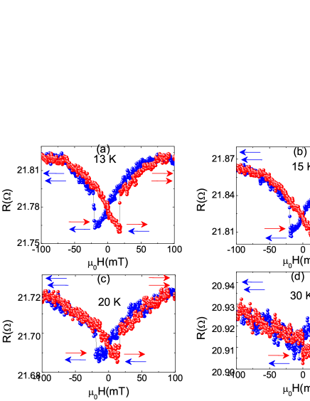
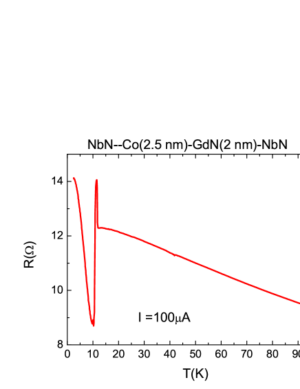
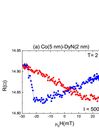
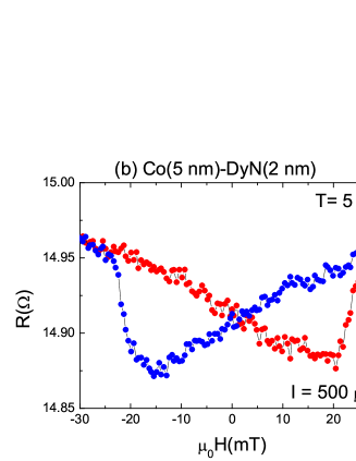
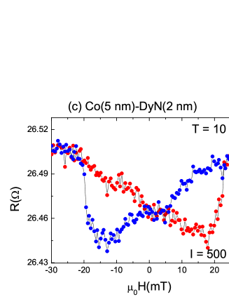
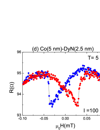
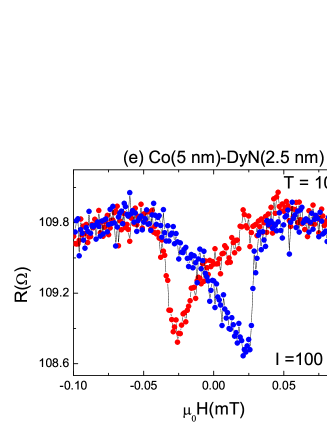
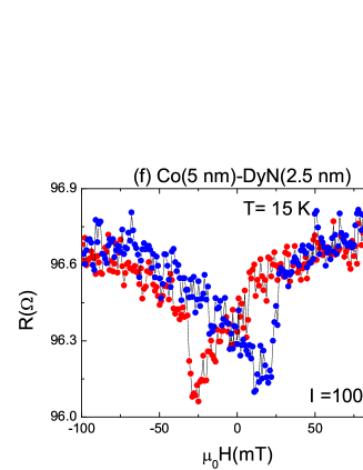
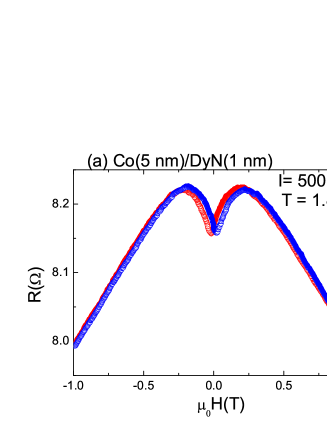
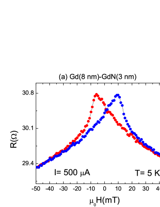
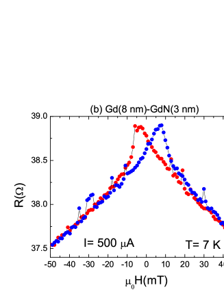
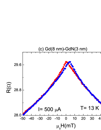
Figure 4(a) shows magnetic field dependence of resistance of the Co(5 nm)-DyN(2 nm) device measured at 2 K. The measurement was done with a bias current A. The resistance was found to increase with magnetic field up to 0.1 T and decrease afterwards. The value of was found to vary from device to device and a complete decreasing trend was observed for devices with thicker DyN (see Supplementary figure SFig. 6). Fig. 4(b) shows field dependence of magnetization measured at 12 and 100 K of a NbN-Co(5 nm)-DyN(4.5 nm)-NbN film deposited at the same time. As 4.5 nm thick DyN have very small magnetic moment compared to Co the M-H loop is mostly dominated by Co. Fig. 4(c) shows field dependence of resistance in the field range 30 mT. One can clearly see resistance switching at 25 mT. This switching appears due to switching of the Co magnetization at 25 mT. Although, coercive field of the NbN-Co(5 nm)-DyN(4.5 nm)-NbN film is 7 mT, resistance switching at 25 mT in the Co(5 nm)-DyN(2 nm) device is due to the reduced dimension of the junction i.e., 7 m 7 m. We found slight variation in the switching field from device to device depending on the thickness of DyN (See supplementary figure SFig. 5). This might be due to the different nitridation of Co which makes effective Co layer thinner. One striking feature to notice is a low resistance state for antiparallel configuration in comparison to parallel configuration. Fig. 4(d) shows similar measurements on Gd(5 nm)-GdN(3 nm) device. A higher resistance for antiparallel state can be seen in this case. In Gd-GdN devices resistance switching was found only at low temperature below 13 K (see supplementary figure SFig.7). This might be due to the absence of a well defined magnetic decoupling layer at the interface between Gd and GdN. In this case a gradient of nitrogen deficiency might separate Gd and GdN layer from each other providing poor magnetic isolator.
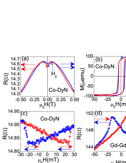
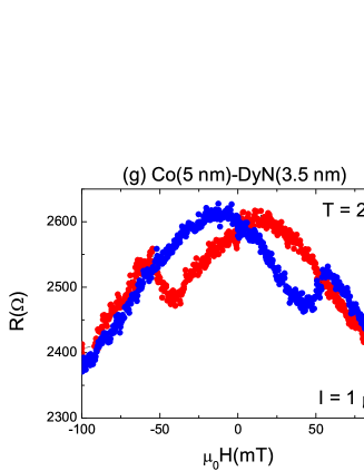
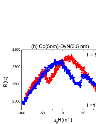
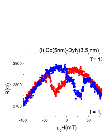
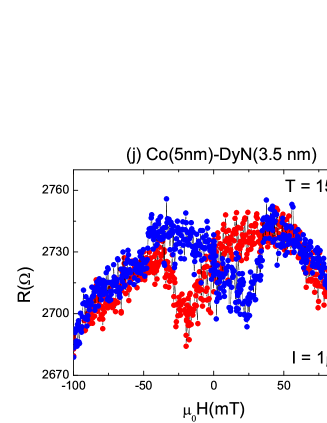
Figure 5 shows R-H loops of the Co(5 nm)-DyN(2 nm) device measured at different temperatures. The resistance switching was found to disappear as temperature was increased to 30 K. This is expected as DyN gets into paramagnetic phase above 35 K. Temperature dependence of switching strongly suggest that the switching arises due to the relative mutual magnetization of Co and DyN. We could not find any switching in devices with thicker DyN ( 3.5 nm). This advocate other sources of switching like AMR of Co or artefact due to device geometry is not responsible for such resistance switching. In samples with thicker DyN the interfacial CoNx is most likely very thick which causes loss of spin polarization of electrons after filtering through DyN. The high field magnetoresistance seen in Figure 4(a,d) seems likely to originate from a field-enhanced magnetisation muduli-arxive and hence an exchange splitting which increases with field.
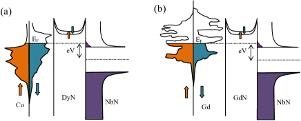
The resistance switching in our devices can be understood considering spin dependent density of states (DOS) of different layers as shown in Fig. 6. When magnetization of Co and DyN are parallel to each other, the up-spin electrons tunneling through DyN experience a lower barrier height compared to down-spin electrons. During tunneling process spin orientation of electrons are conserved, therefore, up and down-spin electrons can tunnel only into spin-up and spin-down states of Co, respectivelyjullier . Similarly when magnetization of Co and DyN are antiparallel to each other down-spin electrons are filtered through. In the case of Co the DOS at the Fermi level for up-spin electrons is lower than DOS for down-spin electronscoey . Therefore the transparency through the DyN-Co bilayer will be higher for antiparallel configuration compared to parallel configuration. This will cause a low-resistance state for situation when magnetization of Co and DyN are antiparallel to each other. This concept can be further verified in Gd-GdN devices where Co is replaced by Gd. Schematic of spin dependent DOS of Gd is shown in Fig. 6(b). In case of Gd the up-spin DOS at is slightly higher than down-spin DOSHarmon . Moreover, unlike Co in the case of Gd tunneling spin polarization is usually found positive experimentallyTedrow . Therefore, one expect a higher resistance for antiparallel configuration compared to parallel configuration as observed in normal spin-valvesjullier . The resistance switching behavior shown in Fig. 4 confirms our interpretation. The sign of the tunnel spin polarization is known to depend strongly on the nature of the interface bonding which is likely different between Co-DyN and Gd-GdN. A detailed band structure calculation is needed to understand different sign of spin polarization in these interfaces.
IV Conclusions
In conclusion, we have fabricated NbN-FM-FI-NbN psuedospin-valve devices (with FM = Co, Gd and FI= DyN, GdN) and made an extensive study of electrical transport measurements. Tunnelling regime was achieved in these devices by optimizing thickness of the DyN layer. In the tunnelling regime quasiparticle tunnelling spectra through the spin-valve were compared to tunneling spectra of NIS tunnel model with a nonmagnetic barrier. We also measured R-H loop of the devices at different temperatures. Clear resistance switching was observed in these devices corresponding to their mutual magnetization direction. The resistance switching was found to be sensitive to density of state (DOS) at the FM-FI interface. In the case of Co a low resistance state was found for antiparallel configuration due to lower spin-up DOS at . A reverse behaviour with high resistance for antiparallel configuration was found for Gd devices. The resistance switching in these spin valve measurements confirm the spin filtering nature of DyN tunnel barrier. Optimization of such devices with ideal deposition condition and interface can lead to huge MR. Thickness of Co (Gd) and barrier transparency of DyN (GdN) can be further tuned to create stronger coupling between the two NbN leading to a S-I-S type device with a spin-valve sandwiched in between.This kind of devices can be tuned between 0 and state through magnetization configuration of the spin valvebaek ; gingrich .
Acknowledgments
This work was done when PKM was supported by the ERC Advanced
Investigator Grant SUPERSPIN during the period June 2012-April
2015. PKM acknowledges Dr X. L. Wang for SQUID measurements and
Device Materials Group (DMG) for experimental facility.
References
- (1) J. Linder and J. W. A. Robinson, Nature Phys. 11, 307 (2015).
- (2) M. G. Blamire and J. W. A. Robinson, Journal of Physics: Condensed Matter 26, 453201 (2014).
- (3) T. Wakamura, H. Akaike, Y. Omori, Y. Niimi, S. Takahashi, A. Fujimaki, S. Maekawa, and Y. Otani, Nature Materials 14, 675(2015).
- (4) Y. Makhlin, G. Schöen, and A. Shnirman, Rev. Mod. Phys. 73, 357 (2001).
- (5) John Clarke and Frank K. Wilhelm, Nature 453, 1031 (2008).
- (6) T. Yamashita, K. Tanikawa, S. Takahashi, and S. Maekawa, Phys. Rev. Lett. 95, 097001 (2005).
- (7) A. I. Buzdin, Rev. Mod. Phys. 77, 935 (2005).
- (8) V. V. Ryazanov, V. A. Oboznov, A. Yu Rusanov, A. V. Veretennikov, A. A. Golubov, and J. Aarts, Phys. Rev. Lett. 86, 2427 (2001).
- (9) T. Kontos, M. Aprili, J. Lesueur, and X. Grison, Phys. Rev. Lett. 86, 304 (2001).
- (10) L. N. Bulaevskii, V. V. Kuzii and A. A. Sobyanin, Pis’ma Zh. Eksp. Teor. Fiz. 25 (1977) 314 [JETP Lett. 25 (1977) 290].
- (11) C. Bell, G. Burnell, C. W. Leung, E. J. Tarte, D.-J. Kang and M. G. Blamire, Appl. Phys. Lett. 84, 1153 (2004).
- (12) J. W. A. Robinson, G. B. Halász, A. I. Buzdin, and M. G. Blamire, Phys. Rev. Lett. 104, 207001 (2010)
- (13) H. Sellier, C. Baraduc, F. Lefloch, and R. Calemczuk, Phys. Rev. Lett. 92, 257005 (2004).
- (14) Mohammad Alidoust and Klaus Halterman, Phys. Rev. B 89, 195111 (2014).
- (15) V. N. Krivoruchko and E. A. Koshina, Phys. Rev. B 64, 172511 (2001).
- (16) F. S. Bergeret, A. F. Volkov, and K. B. Efetov, Phys. Rev. Lett. 86, 3140 (2001); F. S. Bergeret,A. F. Volkov and K. B. Efetov, Rev. Mod. Phys. 77, 1321-1373 (2005).
- (17) Ivana Petkovic, Nikolai M. Chtchelkatchev, and Zoran Radovic,Phys. Rev. B 73, 184510 (2006).
- (18) M. Weides, H. Kohlstedt, R. Waser, M. Kemmler, J. Pfeiffer, D. Koelle, R. Kleiner, E. Goldobin, Appl. Phys. A 89, 613 617 (2007); M. Weides,M. Kemmler, E. Goldobin, D. Koelle, R. Kleiner,H. Kohlsted, and A. Buzdin, Appl. Phys. Lett. 89, 122511 (2006).
- (19) T. I. Larkin, V. V. Bolginov, V. S. Stolyarov, V. V. Ryazanov, I. V. Vernik, S. K. Tolpygo, and O. A. Mukhanov, Appl. Phys. Lett. 100, 222601 (2012).
- (20) G. Wild, C. Probst, A. Marx, and R. Gross, Eur. Phys. J. B 78, 509 523 (2010).
- (21) S. V. Bakurskiy, N. V. Klenov, I. I. Soloviev, V. V. Bolginov, V. V. Ryazanov, I. V. Vernik, O. A. Mukhanov, M. Yu. Kupriyanov, and A. A. Golubov, Appl. Phys. Lett. 102, 192603 (2013).
- (22) S. V. Bakurskiy, N. V. Klenov, I. I. Soloviev, M. Yu. Kupriyanov, and A. A. Golubov, Phys. Rev. B 88, 144519 (2013).
- (23) I. V. Vernik, V. V. Bolginov, S. V. Bakurskiy, A. A. Golubov, M. Y. Kupriyanov, V. V. Ryazanov, and O. A. Mukhanov, IEEE Trans. Appl. Supercond. 23, 1701208 (2013).
- (24) V.V. Ryazanov,V.V. Bolginov, D. S. Sobanin, I. V. Vernik, S. K. Tolpygo, A. M. Kadin, and O. A. Mukhanov, Physics Procedia 36, 35 (2012).
- (25) M. Eschrig, Phys. Today 64, 43 (2011).
- (26) I. Sosnin, H. Cho, V. T. Petrashov, and A. F. Volkov, Phys. Rev. Lett. 96, 157002 (2006).
- (27) J. W. A. Robinson, J. D. S. Witt, and M. G. Blamire, Science 329, 59 (2010).
- (28) T. S. Khaire, M. A. Khasawneh, W. P. Pratt, and N. O. Birge, Phys. Rev. Lett. 104, 137002 (2010).
- (29) R. S. Keizer, S. T. B. Goennenwein, T. M. Klapwijk, G. Miao, G. Xiao, and A. Gupta, Nature (London) 439, 825 (2006).
- (30) M. S. Anwar, F. Czeschka, M. Hesselberth, M. Porcu, and J. Aarts, Phys. Rev. B 82, 100501 (2010).
- (31) J. Wang, M. Singh, M. Tian, N. Kumar, B. Liu, C. Shi, J. K. Jain, N. Samarth, T. E. Mallouk, and M. H. W. Chan, Nat. Phys. 6, 389 (2010).
- (32) P. K. Muduli, A. Pal, M. G. Blamire, Phys. Rev. B 89, 094414 (2014).
- (33) P. K. Muduli, X. L. Wang, J. H. Zhao, M. G. Blamire,arXiv:1410.6741
- (34) A. Pal, K. Senapati, Z. H. Barber, M. G. Blamire, Adv. Mater. 25, 5581 (2013).
- (35) M. G. Blamire, A. Pal, Z. H. Barber, and K. Senapati, Proc. SPIE 8461, 84610J (2012).
- (36) K. Senapati, M. G. Blamire, and Z. H. Barber, Nature Materials 10, 849 (2011).
- (37) T. Nagahama, T. S. Santos, and J. S. Moodera,Phys. Rev. Lett. 99, 016602 (2007).
- (38) Burm Baek, William H. Rippard, Matthew R. Pufall, Samuel P. Benz, Stephen E. Russek, Horst Rogalla, and Paul D. Dresselhaus, Phys. Rev. Applied 3, 011001 (2015).
- (39) P. Leclair, J. K. Ha, H. J. M. Swagten, J. T. Kohlhepp, C. H. van de Vin, W. J. M. de Jonge, Appl. Phys. Lett. 80, 625 (2002).
- (40) J. S. Moodera, T. S. Santos, and T. Nagahama, J. Phys.: Condens. Matter. 19, 165202 (2007).
- (41) Shiro Kawabata, Andrey S. Vasenko, Asier Ozaeta, Sebastian F. Bergeret and Frank W. J. Hekkingb,Blythe, J. Magn. Magn. Mater. 383,157 (2015).
- (42) F. S. Bergeret and F. Giazotto,Phys. Rev. B 88, 014515 (2013).
- (43) Shiro Kawabata, Satoshi Kashiwaya, Yasuhiro Asano, Yukio Tanaka, and Alexander A. Golubov,Phys. Rev. B 74, 180502(R) (2006).
- (44) Kartik Senapati, Mark G. Blamire and Zoe H. Barber,Appl. Phys. Lett. 103, 132406 (2013).
- (45) R. C. Dynes, V. Narayanamurti, and J. P. Garno, Phys. Rev. Lett. 41, 1509 (1978).
- (46) T. M. Klapwijk, G. E. Blonder, and M. Tinkham, Physica (Amsterdam) 109 110B+C, 1657 (1982).
- (47) J. R. Schrieffer and J.W. Wilkins, Phys. Rev. Lett. 10, 17 (1963).
- (48) H. Takayanagi and J. Nitta in Towards the Controllable Quantum States: Mesoscopic Superconductivity and Spintronics, 2002, Page-169
- (49) G. Tkachov, E. McCann, V. I. Falko, Phys. Rev. B 65, 024519 (2001).
- (50) J. P. Pekola, V. Maisi, S. Kafanov, N. Chekurov, A. Kemppinen, Yu. Pashkin, O.-P. Saira, M. Mo tto nen, and J. Tsai, Phys. Rev. Lett. 105, 026803 (2010).
- (51) A. Di Marco, V. F. Maisi, J. P. Pekola, F. W. J. Hekking, Phys. Rev. B 88, 174507 (2013).
- (52) M. Julliere,Phys. Lett. A 54, 225 (1975).
- (53) J.M.D. Coey, Magnetism and magnetic materials, Cambridge University press, Page-149.
- (54) B. N. Harmon and A. J. Freeman,Phys. Rev. B 10, 1979 (1974).
- (55) P. M. Tedrow and R. Meservey,Phys. Rev. B 7, 318 (1973).
- (56) E. Y. Tsymbal, O. N. Mryasov, P. R. Leclar, Journal of Physics: Condensed Matter 15, R109 (2003).
- (57) B. Baek, W. H. Rippard, S. P. Benz, S. E. Russek, P. D. Dresselhaus, Nature Communications 5, 3888 (2014).
- (58) E. C. Gingrich, Bethany M. Niedzielski, Joseph A. Glick, Yixing Wang, D.L. Miller, Reza Loloee, W. P. Pratt, Jr., and Norman O. Birge, Nature Physics 12, 564 (2016).
- (59) M. Matsuoka, K. Ono, T. Inukai,Appl. Phys. Lett. 49 ,977 (1986);K. Oda, T. Yoshio, K. Oda, J. Mater. Sci. 22, 2729 (1987).
Supplementary Information
Spin-polarized quasiparticle tunneling in spin-filter pseudospin-valve devices
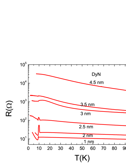
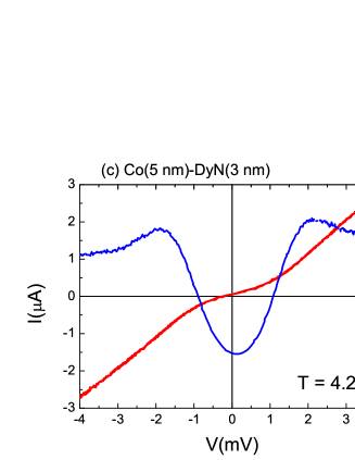
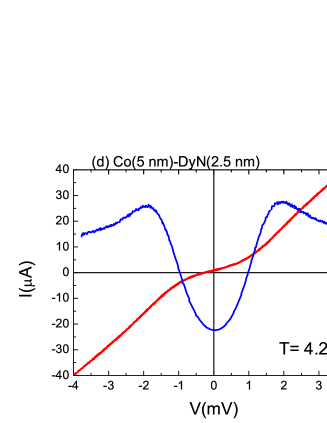
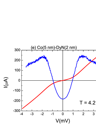
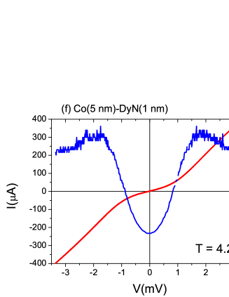
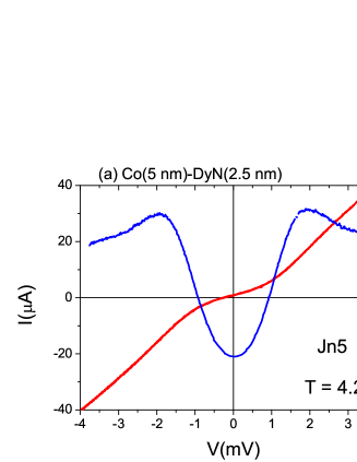
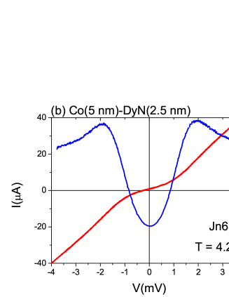
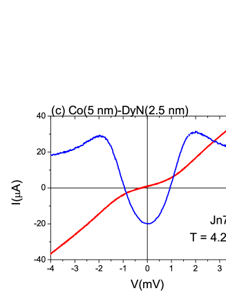
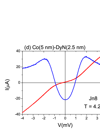
Pseudospin-valve devices were fabricated from NbN-FM-FI-NbN multilayered thin films deposited by DC sputtering method. Here FM = Co and Gd; FI = DyN and GdN. A series of devices were fabricated from Co(5 nm)-DyN(t) multilayer with different thickness of DyN. Few representative devices were fabricated in the configuration Co-GdN and Gd-GdN for comparison. More detailed experiment was done in the Co-DyN series compared to others. In this manuscript a comparison has been made between devices with GdN and DyN for spin-valve measurements. The comparison is reasonable as GdN and DyN are similar ferromagnetic semiconductors with only different spin-filtering efficiency. Measurements done on different devices are summarized in the figures below.
Calculation of Diffusion constant of NbN :
The diffusion constant can be calculated from Einstein relation;
| (2) |
Where is the density of state at Fermi energy and is the resistivity. The diffusion constant can also be written as; , with is Fermi velocity and is the average electron mean free path. For NbN with [Chockalingam et. al. Phys. Rev. B 2008, 77, 214503.] and , we found .
 |
 |
 |
 |
 |
 |
 |
 |
 |
 |
 |
 |
 |
 |
 |
 |
 |
 |
 |
 |
 |
 |
 |
 |
 |
 |
 |
 |