Two-dimensional platform for networks of Majorana bound states
Abstract
We model theoretically a two-dimensional electron gas (2DEG) covered by a superconductor and demonstrate that topological superconducting channels are formed when stripes of the superconducting layer are removed. As a consequence, Majorana bound states (MBS) are created at the ends of the stripes. We calculate the topological invariant and energy gap of a single stripe, using realistic values for an InAs 2DEG proximitized by an epitaxial Al layer. We show that the topological gap is enhanced when the structure is made asymmetric. This can be achieved by either imposing a phase difference (by driving a supercurrent or using a magnetic-flux loop) over the strip or by replacing one superconductor by a metallic gate. Both strategies also enable control over the MBS splitting, thereby facilitating braiding and readout schemes based on controlled fusion of MBS. Finally, we outline how a network of Majorana stripes can be designed.
pacs:
71.10.Pm, 74.50.+r, 74.78.-wMajorana bound states (MBS) are states localized at the edges of topological superconductors AliceaReview; FlensbergReview; BeenakkerReview; TewariReview. They have nonlocal properties that may be utilized for storage and manipulation of quantum information in a topologically protected way BravyiKitaev; BravyiKitaev2; Freedman03. However, the realization of MBS requires superconducting p-wave pairing, which appears only in exotic materials. Therefore, there is currently a search for ways to engineer p-wave pairing by combining s-wave superconductors with strong spin-orbit materials. Recent experiments looked for evidence of MBS in, for example, semiconducting nanowires mourik12; das12; finck12; Rokhinson; deng12; Albrecht2016; Zhang16, topological insulators Williams, and magnetic atom chains Nadj-Perge; Ruby15. These systems may also allow demonstration experiments of the nonlocal properties of MBS, for example using recent suggestions for controlling MBS in prototypical architectures SauBraiding; Flensberg; BeenakkerBraiding; Li16; Aasen15; Hell16. However, to go beyond basic demonstration experiments a scalable and flexible platform for large-scale MBS networks is needed.
Here, we suggest one such flexible platform based on a two-dimensional electrons gas (2DEG) with strong spin-orbit coupling in proximity to a superconductor Shabani16. Such structures, reviewed in Ref. SchaepersBook, have been realized by contacting InAs surface inversion layers Chrestin97; Chrestin99 or InAs/InGaAs heterostructures Takayanagi95; Bauch05 with superconducting Nb or Al. Recently, it has become possible to grow an Al top layer epitaxially Shabani16, forming a clean interface with the 2DEG. The proximitized 2DEG (denoted by pS) develops a hard superconducting gap as revealed by experiments on pS-N quantum point contacts Kjaergaard16 or gateable pS-N-pS junctions Shabani16 with clear signatures of multiple Andreev reflection KjaergaardMAR and nontrivial Fraunhofer patterns Suominen16. The transport properties of these structures have been studied extensively SchaepersBook but their potential as a MBS platform has not.
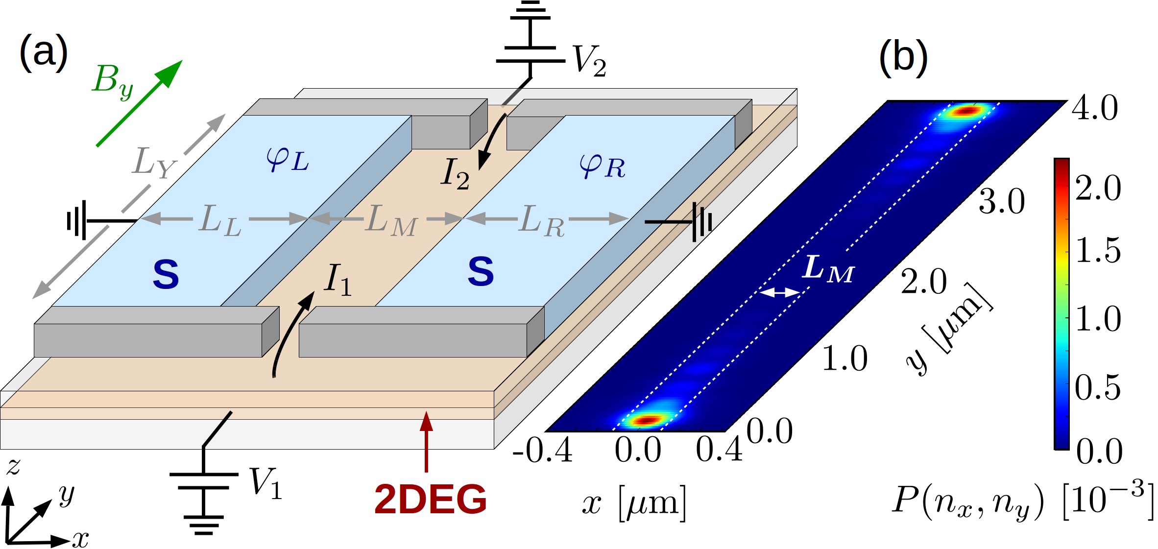
We show how to design and control MBS in a pS system with a stripe of the superconducting layer removed to form an effective one-dimensional topological superconductor. This forms a pS-N-pS junction as sketched in Fig. 1(a), which can be fabricated by standard lithographic techniques. We show, similar to other semiconductor-based setups Sau; Alicea; 1DwiresLutchyn; 1DwiresOreg; Sedlmayr15, that this system undergoes several topological phase transitions when increasing a magnetic field parallel to the stripe for parameters readily available in the lab. We base our findings on a numerical tight-binding calculation of the energy spectrum, the topological invariant, as well as transport calculations Hell162DEGsup. We discuss how the topological energy gap depends on various parameters, which is vital for the topological protection and the manipulation time scales of the MBS. We show that slight modifications of the structure shown in Fig. 1 give a large enhancement of the topological gap and, moreover, grant electrical control over the phase-transition point. The key is to break the inversion symmetry perpendicular to the stripe direction, and we study two methods to accomplish this: (i) a phase bias (generated by a supercurrent) across the stripe, or (ii) replacement of one of the superconducting top layers by a gate electrode. Both methods allow to fuse the MBS electrically, which can be used to manipulate MBS in 2DEG structures. In the last part of the paper, we discuss designs of more advanced MBS networks for fusion-rule testing and braiding.
Model. We model the (unproximitized) 2DEG by a single electron band with effective mass and electro-chemical potential . The device has a finite extension with and , where it is described by the Bogoliubov-de Gennes Hamiltonian ():
| (1) | |||||
In the second line, we add the Rashba spin-orbit coupling (with velocity ) and the Zeeman energy () due to a magnetic field along the stripe. The Hamiltonian acts on the four-component spinor containing the electron and hole components for spin . The Pauli matrices and () act on particle-hole and spin space, respectively.
We include the proximity effect of the superconducting top layer within the Green’s function formalism. Integrating out the superconductor in the wide-band limit, the Green’s function of the 2DEG is given by SauProximityEffect; StanescuProximityEffect; Hansen16
| (2) |
with self energy
| (3) |
The self energy is zero in the stripe region, , and nonzero under the two superconducting layers coupled to the 2DEG with symmetric tunneling rates . In this way, we only make an assumption about the superconducting order parameter in the metallic top layer, while the superconducting pairing in the 2DEG is determined by Eq. (2). The two top layers are assumed to have the same gap but possibly different phases and . Such a phase bias can be realized experimentally by running a supercurrent across the stripe. Our self energy does not include a proximity-induced shift of the chemical potential under the superconductor. This is motivated by recent experiments KjaergaardMAR showing that pS-N-pS junctions have a high transparency, which indicates a rather small mismatch in Fermi velocities.
Symmetry class and topological invariants. We first investigate the general topological properties of the stripe. Since its aspect ratio is large (), the system is quasi-1D, similar to coupled Wakatsuki14; Kotetes15 or multiband StanescuProximityEffect; Lutchyn11Multiband nanowires. The topological properties are in general determined by the zero-frequency Green’s function Wang13; Budich13. The self energy takes in this limit the form of a non-dissipative pairing term and the topological properties are thus determined by Wang14
| (4) |
This effective Hamiltonian respects particle-hole symmetry since it anticommutes with the antiunitary operator ( denotes the complex conjugation). If no generalized time-reversal symmetry is present, the system is thus in symmetry class D () with a topological invariant Altland97; Ryu10.
However, our system can also be in the higher-symmetry class BDI with an integer topological invariant . This is the case if the system has spatial symmetry in -direction (), assuming here no disorder in the -direction. The effective Hamiltonian then possesses an additional generalized ’time-reversal’ symmetry: it commutes with the antiunitary operator ( is the reflection in -direction) 111The time-reversal and particle-hole conjugation operator are not unique since has an additional unitary symmetry , where is the reflection operator in direction.. This symmetry holds even in the presence of a phase bias Pientka16. Unlike the physical time reversal, the generalized operator squares to identity, . If both - and -symmetry are present, also chiral symmetry is present, i.e., anticommutes with .
To predict a topological phase transition, we compute topological invariants (BDI) and (D). To obtain , we follow Ref. Tewari12TopInv: Because the chirality operator satisfies , its only eigenvales are and in these two subblocks the Hamiltonian is off-diagonal (since ):
| (9) |
The invariant follows from the winding number of the phase of the determinant of , as . The integer characterizes the number of MBS which appear at the boundaries of a long stripe with two topologically trivial regions.
When -symmetry is broken, an even number of MBS on the same boundary couple to each other, turning them into finite-energy modes. This leaves either zero or one MBS, characterized by the invariant . We compute in the standard way 1DwiresKitaev by representing as a matrix in Majorana representation. The topological invariant is given by the relative sign of the Pfaffian of at the -invariant points and Hell162DEGsup.
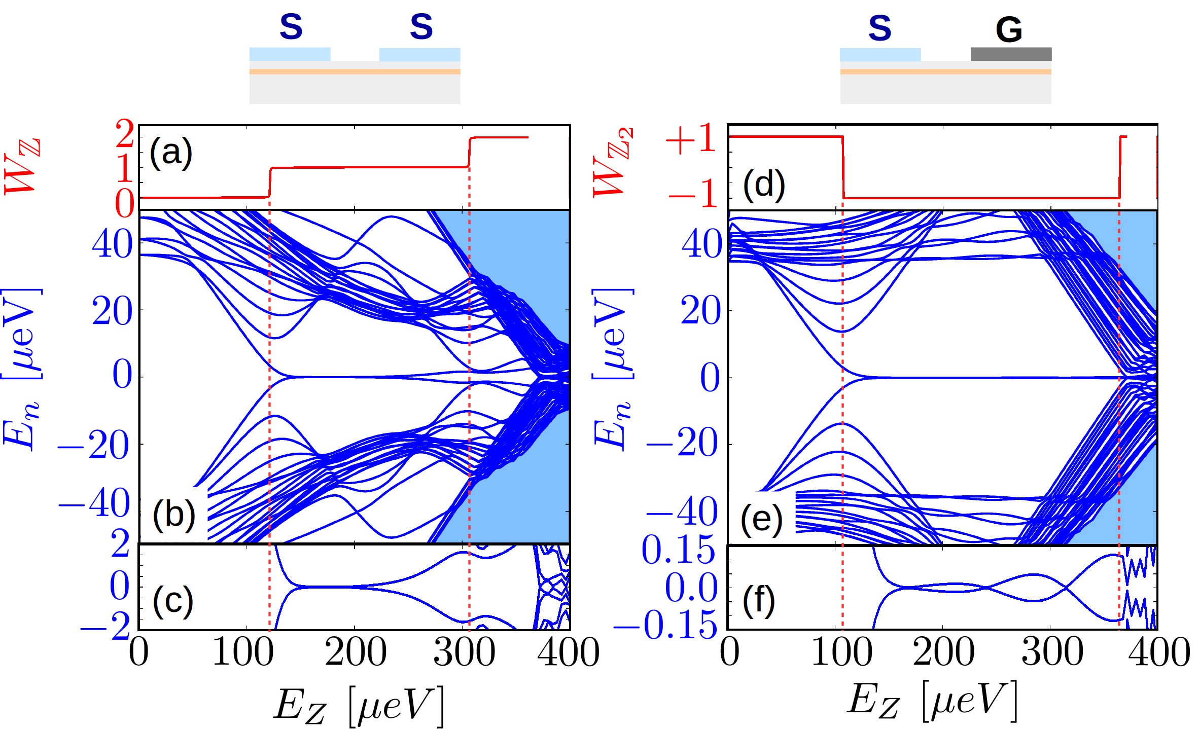
Topological phase transition. Figure 2 demonstrates that the stripe region undergoes a topological phase transition for material parameters in the range of recent experiments Shabani16; Kjaergaard16; KjaergaardMAR. We obtain our results numerically using a tight-binding approximation of the effective Hamiltonian (S17) Ferry97Book; Hell162DEGsup.
We first discuss the -symmetric case (left panels of Fig. 2). Starting from the topologically trivial regime (), one can identify a first phase transition at Zeeman energy eV [, Fig. 2(a)]. For a -factor of about 10 Kjaergaard16, this requires a magnetic field of 200 mT, much lower than the critical fields in Al thin films Tedrow81. At first sight it may be surprising that the critical Zeeman energy is smaller than the induced superconducting gap under the superconducting top layers. The reason is that the Andreev bound states in the stripe experience the pairing potential only where they penetrate into the proximitized region and, as a consequence, the effective gap is smaller than .
In agreement with the change in , a pair of states comes close to zero energy around [Fig. 2(b)]. The wave functions of these states are localized at the ends of the stripe [Fig. 1(b)] and, because of the finite length of the stripe, their energies oscillate around zero [Fig. 2(c)]. From Fig. 2(b), we extract an energy gap to excited states – the topological energy gap – of about 20eV, which corresponds to about 200 mK.
A second phase transition takes place for eV [, Fig. 2(a)], where, for a finite stripe length, a second pair of states approaches zero energy [Fig. 2(b)]. However, for the parameters chosen in Fig. 2, the states remain split in energy because the regime is close to the breakdown of the induced superconducting gap (at eV). By increasing the stripe width, one can reach the regime of two MBS for lower Hell162DEGsup.
To confirm the presence of the MBS, one can probe the conductance of the stripe by two quantum point contacts [see Fig. 1(a)]. We compute the transport spectrum numerically Hell162DEGsup and find a zero-bias peak in the local conductance with a peak value up to ZeroBiasAnomaly1; Nilsson08; Tewari08 while the nonlocal response is strongly suppressed for uncoupled MBS, different from extended Andreev bound states.
For future applications for topological quantum-information processing, it is desirable to enhance the topological energy gap as much as possible. This can be achieved, for example, with an asymmetric device structure as depicted above Fig. 2(d): One replaces one of the superconducting layers by a top gate that creates a potential barrier for the electrons in the 2DEG underneath. We model this here by terminating the system at the right end of the stripe setting . The Hamiltonian is now in class D since -symmetry is broken. The invariant indicates a phase transition around eV [, Fig. 2(d)] and a single pair of states approaches zero energy [Fig. 2(e)]. Compared with the symmetric device, their energy splitting is much smaller [eV, Fig. 2(f)] and the topological gap is increased [eV, Fig. 2(e)]. An asymmetric device design thus seems promising for stabilizing MBS.
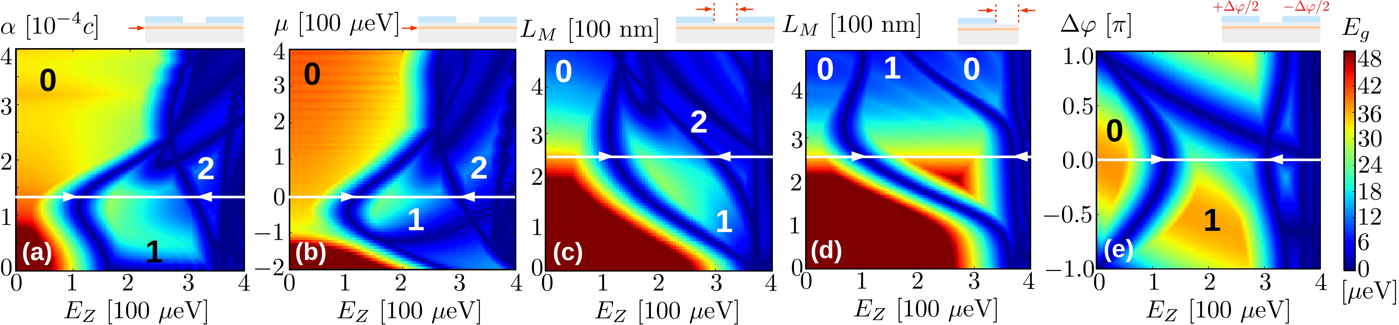
Phase diagrams and topological gap. To study the optimal conditions for observing MBS in experiments more systematically, we next investigate the topological energy gap (see caption of Fig. 3). Both the gap and the boundaries of the topological phases given by the zero-gap condition exhibit a nontrivial dependence on the different parameters [Fig. 3]. Due to the finite-frequency and finite-size effects, the actual topological gap may be smaller, but by comparing with transport calculations (including both effects) we find only a small reduction Hell162DEGsup.
We first focus on the case with inversion symmetry [Figs. 3(a)–(c)]. The phase-transition point depends on the spin-orbit coupling [Fig. 3(a)]; however, a change in can be compensated by a shift of the electro-chemical potential Pientka16. By contrast, the topological gap depends in a nontrivial way on : It becomes maximal around and is is strongly suppressed for for the experimentally relevant parameters used in Fig. 3(a) for fixed . Fortunately, the spin-orbit velocities extracted from current experiments Shabani16, , are close to being optimal. From Fig. 3(b) we see that it is crucial to tune the electro-chemical potential near zero if no phase bias is applied, which requires a strong gate coupling, similar to the situation for nanowires 1DwiresLutchyn; 1DwiresOreg. Finally, we find that a stripe width of around 200 nm is optimal for a large topological gap [Fig. 3(c)].
As mentioned before, breaking the generalized -symmetry can further increase the topological gap. For example, the asymmetric, gated device [Fig. 3(d)] exhibits a topological gap that can be larger by a factor of up to 2. However, the gap can also be manipulated without breaking the generalized -symmetry in a phase-biased device [Fig. 3(e)]. Depending on the sign of the phase bias , the direction of the supercurrent is reversed, which through the spin-orbit term affects the spectrum differently for a nonzero Zeeman term. This can both increase and decrease the gap, which could be used to determine the sign of experimentally. Second, both for gating and phase bias the regime of MBS can be reached for smaller Zeeman energies [see in Fig. 3(d) and in Fig. 3(e)]. Finally, the phase transition point can be moved in-situ, either by changing through the gate or by a supercurrent controlling .
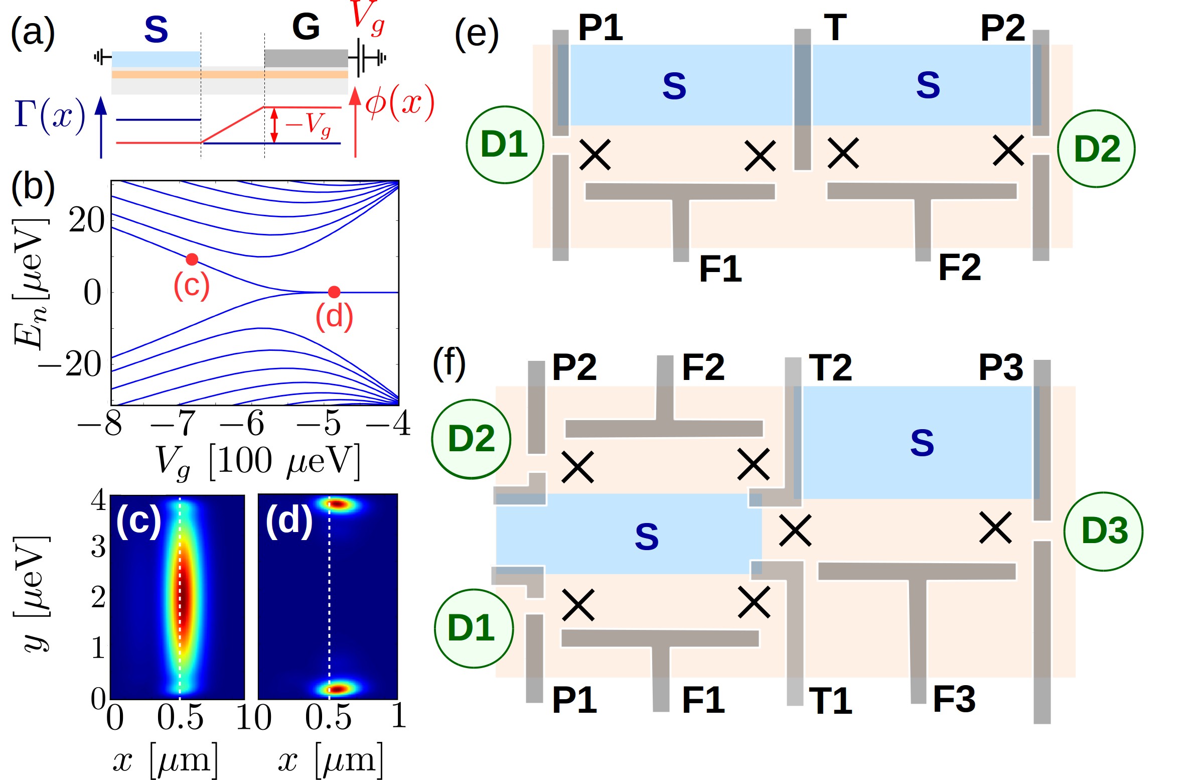
Electrical control for MBS networks. The above-mentioned sensitivity of the phase-transition point suggests the possibility to control the coupling of the MBS electrically. To illustrate this, we assume that the nearby top gate creates a triangular confining potential for the MBS [Fig. 4(a) and (b)]. By increasing the potential drop across the stripe by lowering , the MBS can be tuned from localized boundary modes [Fig. 4(d)] at zero energy into modes at finite energy and delocalized along the stripe [Fig. 4(c)]. Controlling the MBS coupling with a gate can be used for the initialization and readout of the MBS also in larger networks of MBS stripes. Readout requires a way to detect the fermion parity of the MBS, which can be achieved by charge detection Ben-Shach14, possibly using an auxiliary quantum dot Hoving16readout.
To implement a qubit in a 2DEG structure, one can segment the MBS stripe into two parts using a finger gate [Fig. 4(e)]. Tuning this gate controls the coupling of the MBS in the middle (indicated by crosses), which could be used to carry out fusion-rule and coherence-test experiments Aasen15; Hell16. Finally, in order to realize braiding of MBS similar to Refs. SauBraiding; BeenakkerBraiding; Aasen15; Hell16, one needs to couple three MBS. Our numerical simulations indicate Hell162DEGsup that the topological phase is stable against a rotation of the magnetic field of about 10∘ away from the stripe direction. We therefore suggest using a ’tuning-fork’ design [Fig. 4(f)] instead of a T-junction structure usually considered for braiding-type experiments. This keeps the stripes in parallel.
Conclusion and outlook. We have shown that 2DEG structures with strong spin-orbit coupling, proximity-induced superconductivity, and magnetic fields provide an alternative platform hosting MBS that is readily available in the lab. A phase bias or a gate electrode can be used to couple the MBS in the stripe by electrical means. Together with the technological advantage of flexible top-down fabrication of 2DEG structures, this might open the door for larger MBS networks. Note: After the first version of this preprint appeared, a preprint appeared that treats a device similar to the one considered here Pientka16.
Acknowledgements.
We acknowledge stimulating discussions with M. Kjaergaard, P. Kotetes, C. M. Marcus, F. Nichele, and H. J. Suominen, and support from the Crafoord Foundation (M. L. and M. H.), the Swedish Research Council (M. L.), and The Danish National Research Foundation. Computational resources were partly provided by the Swedish National Infrastructure for Computing (SNIC) through Lunarc, the Center for Scientific and Technical Computing at Lund University.References
Two-dimensional platform for networks of Majorana bound states:
Supplemental Material
Michael Hell
Martin Leijnse
Karsten Flensberg
I Numerical approach
In this Section, we explain our numerical procedure to compute the energy spectrum, topological invariants, and topological gaps presented in the main part. Our approach is based on a tight-binding approximation of the effective Hamiltonian [Eq. (4) in the main part], which we introduce first. Since diagonalizing the 2D tight-binding Hamiltonian is computationally demanding, we speed up our calculations by solving the eigenvalue problem in two steps: We first solve the one-dimensional tight-binding problem transverse to the stripe direction, project on a number of low-energy modes, and in the last step solve a second one-dimensional tight-binding problem along the stripe direction. We finally discuss how the different symmetry classes for symmetric and asymmetric devices manifest in the energy spectrum when a second phase transition appears.
I.1 Two-dimensional tight-binding model
The tight-binding model for our calculations is obtained by discretizing the continuous spatial coordinates as a lattice with points in the direction (perpendicular to the stripe) and points in the direction (along the stripe). The lattice points are given by with , and lattice constants . Due to the discretization, we have to replace the derivatives in the Hamiltonian by finite differences:
| (S1) | |||||
| (S2) |
Analogous formulas apply for the derivative. Using this procedure, we can rewrite the inverse retarded Green’s function [Eq. (2) in the main part] in tight-binding approximation. Using the hopping amplitudes
| (S3) |
it reads
| (S4) | ||||||
Here, denotes a state with an electron () or hole () with spin localized at lattice point . We introduce the short-hand notations , , , the Z factor SauProximityEffect
| (S5) |
and express the frequency-dependent superconducting pairing as:
| (S6) | |||||
In the limit , the Green’s function is related to the effective Hamiltonian [Eq. (4) in the main part] by . Both and are thus represented by matrices for lattice points with spin () and particle-hole () degree of freedom. For inferring the topological properties, we use , while we use the full Green’s function later for our transport calculations (see Sec. II). The eigenstates of are represented by a 4-component vector at each lattice site
| (S15) |
and the probability densities shown for the eigenstates in Figs. 1(b), 4(c), 4(d) in the main part are given by
| (S16) |
I.2 Numerical diagonalization with low-energy projection
The matrix for the effective Hamiltonian can, in principle, be diagonalized by standard numerical procedures. However, the number of lattice points that can be treated is limited by computational power and we therefore perform the diagonalization in two steps with an intermediate approximation. For this purpose, we split the effective Hamiltonian into two parts:
| (S17) | |||||
The first transverse part contains all terms that do not change [related to the first three lines in Eq. (S4)] and the second part contains the hopping terms in the direction [related to the fourth line in Eq. (S4)]. We note that the effective 1D tight-binding Hamiltonian is independent of . We first diagonalize this part as with standard procedures, where contains the eigenvalues of . We next apply the unitary transformation to Hamiltonian (S17), which yields
with hopping matrix .
We next apply our approximation: We neglect high-energy eigenstates of , i.e., we project onto the eigenvalues closest to zero energy, somewhat similar to Ref. Disorder7. We denote the corresponding projector in the following by . Applying reduces the dimension of the matrices and :
with and , both matrices. We include into the projection not only bound states confined in the stripe but also a part of the spectrum above the gap. This is necessary because the hopping matrix couples subgap states of to states above the (induced) superconducting gap. Moreover, we find that low-energy spectrum of the full effective cannot be reproduced in a satisfactory way without these states above the gap. For all plots we chose except for Fig. 4 where we chose . Diagonalizing Eq. (I.2) yields then the energy spectra shown in Fig. 2 in the main part. We note that the results for the bound states of the stripe do not depend on the widths and of the proximitized regions as long as the wave functions have decayed at the boundary of the simulated area.
I.3 Topological invariants
We next explain how to compute the topological invariants (symmetry class D) and (symmetry class BDI), which we discussed in the main part. This calculation does not require an additional projection as above since the topological properties are inferred from a corresponding one-dimensional bulk system. This bulk system is obtained by extending the stripe to infinity in the positive and negative direction. We can thus replace the derivative by the wave vector and obtain the following effective Hamiltonian in tight-binding representation in the direction:
The computation of follows along the lines of Ref. Tewari12TopInv as explained in the main part. Since the Hamiltonian is represented by a finite-dimensional matrix, we can also compute the winding phase below Eq. (5) in the main part by computing the determinant of a finite-dimensional matrix.
When -symmetry is broken, an even number of MBS couple to each other, turning them into finite-energy modes. This leaves over zero or one MBS, characterized by the invariant . We compute in the standard way 1DwiresKitaev by first representing as a matrix in Majorana representation:
Here, we introduced new states (suppressing the index, which remains unaffected),
| (S30) |
with the unitary matrix 222We define since this simplifies the form of Eq. (S36). Note that the matrix characterizes how the electron annihilators can be expressed in terms of Majorana operators . The states, by contrast, are related through the complex-conjugate matrix analogous to the electron creation operators.
| (S35) |
The matrix is related to the Hamiltonian matrix by
| (S36) |
and satisfies the relations
| (S37) | |||||
| (S38) |
The first of these relations follows simply from the Hermiticity of the Hamiltonian, . The second relation is a consequence of the the particle-hole symmetry, , with the particle-hole conjugation operator as introduced in the main part. Equation (S38) can be shown by complex conjugating Eq. (S37) and exploiting the relation .
The invariant can be next expressed as 1DwiresKitaev
| (S39) |
where denotes the Pfaffian. Note that for the time-reversal invariant momenta, the matrix is real and antisymmetric according to Eqs. (S38) and (S37). Equation (S39) is thus well-defined. Since the kinetic-energy term dominates for large , the Hamiltonian approaches that of quasi-free electrons and the Pfaffian and evaluating Eq. (S39) thus amounts to computing the Pfaffian for . Provided the Hamiltonian is in the higher-symmetry class BDI, is still a topological invariant, which is related to by Tewari12TopInv
| (S40) |
I.4 Symmetry class BDI vs. D
In the main part, we discussed that the symmetric device structure is in symmetry class BDI and can have an integer number of MBS (), while the asymmetric device structure is in symmetry class D and can have zero or one MBS (). However, in Fig. 2 of the main part, the two MBS for case BDI are rather “undeveloped” since they appear close to the closing of the superconducting gap. Here we show that the regime of two MBS can instead be fully developed by increasing the stripe width .
Increasing the stripe width is favorable because this lowers the confinement energy of the second-lowest transverse mode in the Majorana stripe. This mode evolves into the second pair of MBS. In this way, the phase-transition is shifted to lower Zeeman energies and a larger topological energy gap can be achieved. A larger gap reduces the localization length of the MBS wave functions, which reduces their energy splitting due to finite wave-function overlap.
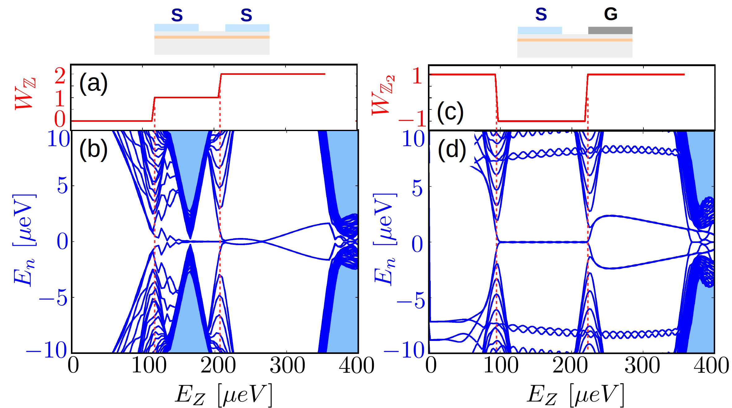
Following the above reasoning, we changed the dimensions of the stripe from 250 nm 4 m for Fig. 2 in the main part to nm 20 m in Fig. S1 shown here. This lowers the critical Zeeman energy for the second phase transition point, , to eV [Fig. S1(a)]. This is around 100 eV lower than for the smaller stripe width [Fig. 2(a) in the main part]. Around the critical Zeeman field, a second pair of states approaches zero energy for a symmetric device [Fig. S1(b)]. If instead the -symmetry is broken, the number of MBS alternates between zero or one as we show here for an asymmetric device [Fig. S1(d), here taking nm 20 m]. The changes in the energy spectrum coincide with the changes in the invariant [Fig. S1(c)]. Different from the regime in Fig. S1(b), the states do not oscillate around zero energy but remain at finite energy instead.
Although the above findings are more of theoretical interest at this point, they may also have experimentally relevant implications. The regime of a single MBS is probably more suitable for potential applications for quantum computation. One would like to avoid the presence of two MBS pairs since this complicates initialization and readout and the MBS could couple to each other under non-perfect conditions breaking the -symmetry. In this respect, an asymmetric device structure would avoid such complications and turns out to be favorable. It may also be interesting to study the transition between the two symmetry classes by simply changing the stripe width. Hence, a 2DEG platform provides an interesting experimental playground also from a fundamental physics perspective.
II Transport spectra
The subgap spectrum of the Majorana stripe can be investigated experimentally most easily by transport measurements. We therefore complement our discussion in the main part, which focuses on the energy spectrum, by a calculation of the transport features. The situation we consider is sketched in Fig. 1(a) in the main part: One could probe the Majorana stripe by connecting it to two quantum points contacts and measure the response of the currents flowing from lead into the stripe as a function of the voltages applied to lead . In short, we find a zero-bias peak in the local conductance with a peak value up to , similar to nanowires ZeroBiasAnomaly1; ZeroBiasAnomaly3; ZeroBiasAnomaly4; ZeroBiasAnomaly5; ZeroBiasAnomaly6. By contrast, the nonlocal response is strongly suppressed as long at the two MBS are uncoupled but appears when the MBS are coupled due to wave-function overlap, also analogous to nanowires ZeroBiasAnomaly1; Nilsson08; Tewari08; Zocher13; Liu13. We first explain our numerical approach in Sec. II.1 and discuss our results for the conductance in Sec. II.2.
II.1 Scattering theory
To compute the transport properties, we apply a scattering-matrix formalism to the setup sketched in Fig. 1 in the main part. The scattering region is formed by the entire 2DEG part, which is in total connected to four terminals: two normal leads (terminals 1 and 2) via the quantum point contacts and two superconductors as top layers on the 2DEG. Here, we are interested only in the transport through terminals 1 and 2 and compute the conductance matrix
| (S41) |
Due to current conservation in the steady state, the current flowing into the superconductors is given by , which is in general nonzero. Since we assume the superconductors to be grounded, Coulomb-blockade effects are suppressed in the stripe and a scattering approach may be applied.
We use a simple model for the leads and assume that only one transverse mode can propagate through each quantum point contact. The two leads thus provide together eight incoming and outgoing channels, accounting for electrons and holes () with spin . The scattering matrix is then an matrix,
| (S44) |
with reflection matrices and transmission matrices . These matrices can be divided into electron- and hole sectors:
| , | (S49) |
We compute the scattering matrix by employing the Weidenmüller-Mahaux formula Hansen16; Beenakker15rev; Aleiner02rev:
| (S50) |
The formula incorporates the the retarded Green’s function of the scattering region, which is a matrix in our tight-binding model with and sites in the and direction, respectively (see Sec. I.1). We note that Eq. (S50) includes the full frequency dependence of the self energy contained in the Green’s function and accounts for a finite extension of the system in the direction. This provides a more accurate estimate of the topological energy gap than the effective Hamiltonian [Eq. (4) in the main part], which neglects finite-frequency and finite-size effects.
The coupling to the leads is described by the matrix , which contains the couplings of each site of the scattering region to the lead channels:
| (S51) | |||||
The first line expresses that lead couples to the bottom-most row of sites , while lead couples to the top-most row of sites (). The coupling is restricted in the transverse direction to the sites inside the Majorana stripe, which we denote in a short-hand way by (in practice, the coupling is also determined by the width of the quantum-point contact). The Kronecker symbols in the second line express that the tunneling is spin-conserving and does not mix particles and holes. Moreover, both leads are coupled to the stripe symmetrically with the same particle-hole and spin-independent tunneling rate . Our simple model ignores the effects of spin-orbit coupling and magnetic field in the leads.
Once the scattering matrix is computed, the differential conductance follows from the formula Lesovik97:
with the spectral conductance
| (S53) | |||||
| (S54) |
and Fermi function for lead at temperature (we assume the reference electro-chemical potential of all leads to be zero).
In general, the spectral conductance can have an explicit voltage dependence since the voltages may change the tunnel coupling or the spectral properties of the scattering region. We ignore this effect here so that the conductance follows as a folding of the spectral conductance with the derivative of the Fermi function. For zero temperature , as assumed in the following, the Fermi function becomes a delta function and we get .
Using Eqs. (S53) and (S54), one can decompose the zero-temperature conductance into contributions related to different transport processes,
| (S55) |
where we use as an index but in mathematical expressions. Since we use this decomposition for our interpretation of the conductance spectra shown below in Sec. II.2, we briefly review these processes. An electron incoming from lead 1 has four possibilities as we discuss next. (i) : It can be normally reflected as an electron leading to no current [the contribution from cancels with the term in Eq. (S53)]. (ii) : It can be Andreev-reflected as a hole, which transfers a Cooper pair into the stripe contributing to [the contribution from adds to the term in Eq. (S54)]. (iii) : It can be transmitted as an electron into lead 2 by direct charge transfer. This process contributes positively to (contained in ) and negatively to . (iv) : It can be cross-Andreev reflected as a hole into lead 2, leaving a Cooper pair in the stripe. This process contributes positively both to and .
II.2 Transport spectra: Local vs. nonlocal current response
Our results for the local (nonlocal) conductance (), are summarized in Fig. S2, for both the symmetric (left) and asymmetric (right) device structure as investigated in the main part. The peak positions in the conductance spectrum closely resemble the energy spectrum of the devices [Figs. 2(b) and (e) in the main part]. The individual contributions from different transport processes [see Eq. (S55)] are shown in Fig. S3 and the stripe-length dependence is shown in Fig. S4.
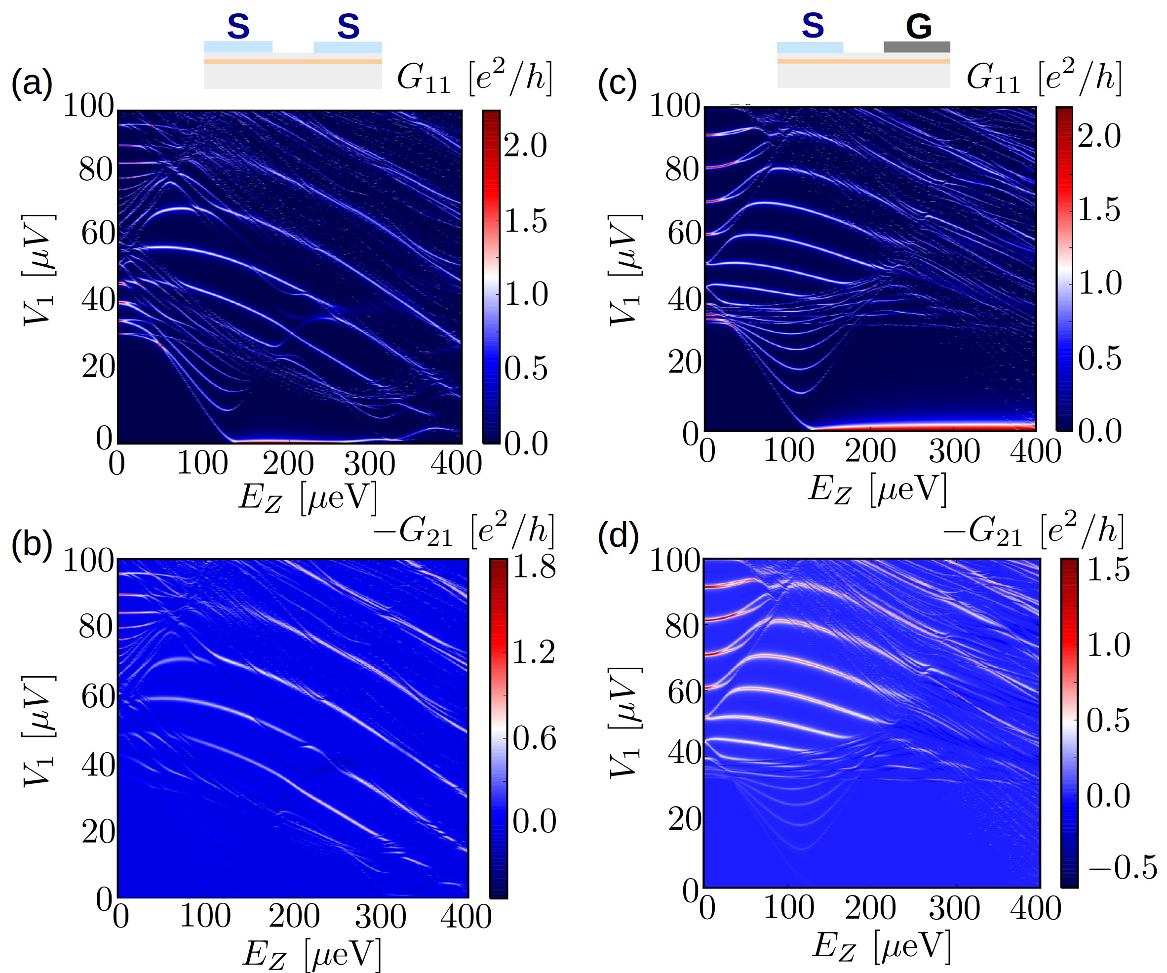
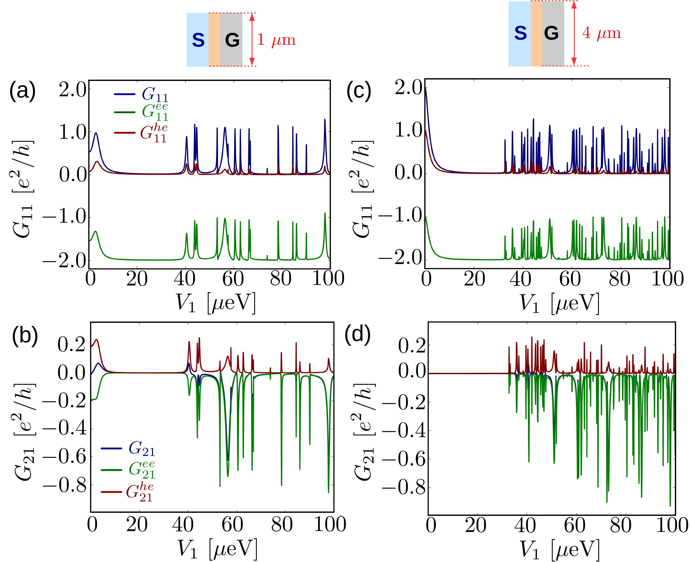
In our discussion, we first focus on the local response , shown in the upper panels of Figs. S2 and S3. Similar to nanowires, ZeroBiasAnomaly1; ZeroBiasAnomaly3; ZeroBiasAnomaly4; ZeroBiasAnomaly5; ZeroBiasAnomaly6, we identify a zero-bias peak for a large range of Zeeman energies [Fig. S2(a) and (c)]. The conductance peak reaches and the peak width is somewhat smaller than the tunnel coupling to the leads [Fig. S3(c)]. The reason for this is that the leads couple only to the first row of sites in the stripe but the MBS wave functions are nonzero over a larger number of sites along the stripe direction [see Fig. 1(b) in the main part].
From inspecting the individual contributions to the conductance, we can see that normal electron reflection contributes with , while the local Andreev reflection contributes with [Fig. S3(c)]. This result can be interpreted as consequence of the spin polarization of the MBS: When the spin of the incoming electron matches the spin of MBS, a local Andreev reflection process happens and a Cooper pair is transferred to the stripe. However, when the incoming electron has opposite spin direction, it must be normally reflected. Hence, the latter species of electrons does not contribute to the current. This explains why the MBS conductance peak rises to .
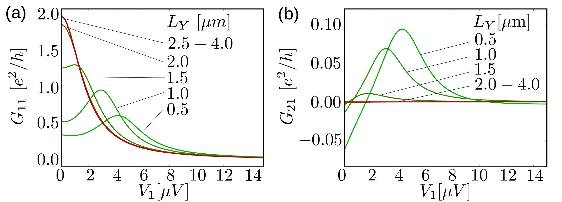
We further find that a zero-bias peak appears only when the stripe length exceeds m [Fig. S4(a)]. When reducing the length, the zero-bias peak moves to finite bias [see Fig. S4(a) for m]. The reason for this behavior is that the MBS wave functions at the two ends start to overlap, which leads to a coupling between the MBS and shifts their energy to a finite value. At the same time, the local Andreev reflection is increasingly suppressed compared to the case of zero-energy modes [Fig. S3(d)]. The peak value of the conductance is thus suppressed far below .
We next discuss the nonlocal conductance depicted in the lower panels of Figs. S2 and S3. Starting again with a long stripe, we see that the zero-bias peak is clearly absent in the nonlocal response in contrast to the local response [Fig. S2(b) and (d)]. Moreover, the two contributions for direct charge transfer, , and crossed Andreev reflection, , are both individually suppressed for low energies [Fig. S3(d)]. In agreement with the literature Nilsson08, we verified that the ratio in the limit of long stripes when the particle and hole weight of the MBS are equal (not shown). The reason for the strong suppression is the exponentially small overlap of the localized MBS. This is different from other subgap states, which are extended along the stripe and thus allow for nonlocal transport [Fig. S2(b) and (d)]. The transport through these states is dominated by direct charge transfer [Fig. S3(d)].
The nonlocal conductance spectra are particularly useful to estimate the topological gap when accounting for finite-frequency corrections to the self energy. The topological gap obtained from the positions of first finite-bias peak [Fig. S3(b) and (d)] at about V are close to the topological gaps of about V obtained in the main part without finite-frequency corrections [Fig. 3(c) and (d)]. This shows that the reduction due to finite-frequency corrections is indeed rather small. This is also expected because finite-frequency corrections play an important role only when energies approach the superconducting gap [see Eq. (S6)].
Finally, for shorter stripe lengths m, a low-energy peak appears in the nonlocal response at the same energy as in the local response [Fig. S4(b)]. This is consistent with the picture of an increased MBS wave function overlap. The net nonlocal current results from a competition of direct charge transfer contribution and the contribution from crossed Andreev reflection. This leads to a considerable reduction of the net current [Fig. S3(b)]. However, direct charge transfer dominates in particular for larger bias voltages because the character of the finite-energy states becomes more and more electron- and less hole-like.
In summary, our transport calculations indicate that the MBS in the Majorana stripe could be probed experimentally similar to nanowire setups. However, we assumed in our calculations that the transport is coherent over the entire stripe length, which is probably hard to achieve in an experiment. It could therefore be interesting to investigate how stable the above transport features would be when including disorder into the calculation. Moreover, the probes are exposed to magnetic fields and exhibit spin-orbit coupling, which may also affect the transport features.
III Magnetic-field angle dependence of topological gap
In this Section, we investigate the stability of the topological phase and the topological gap when the magnetic field is rotated in the plane of the 2DEG. For this purpose, we replace the Zeeman term in Eq. (I.3) by
The case corresponds to a magnetic field along the stripe, which we investigated so far.
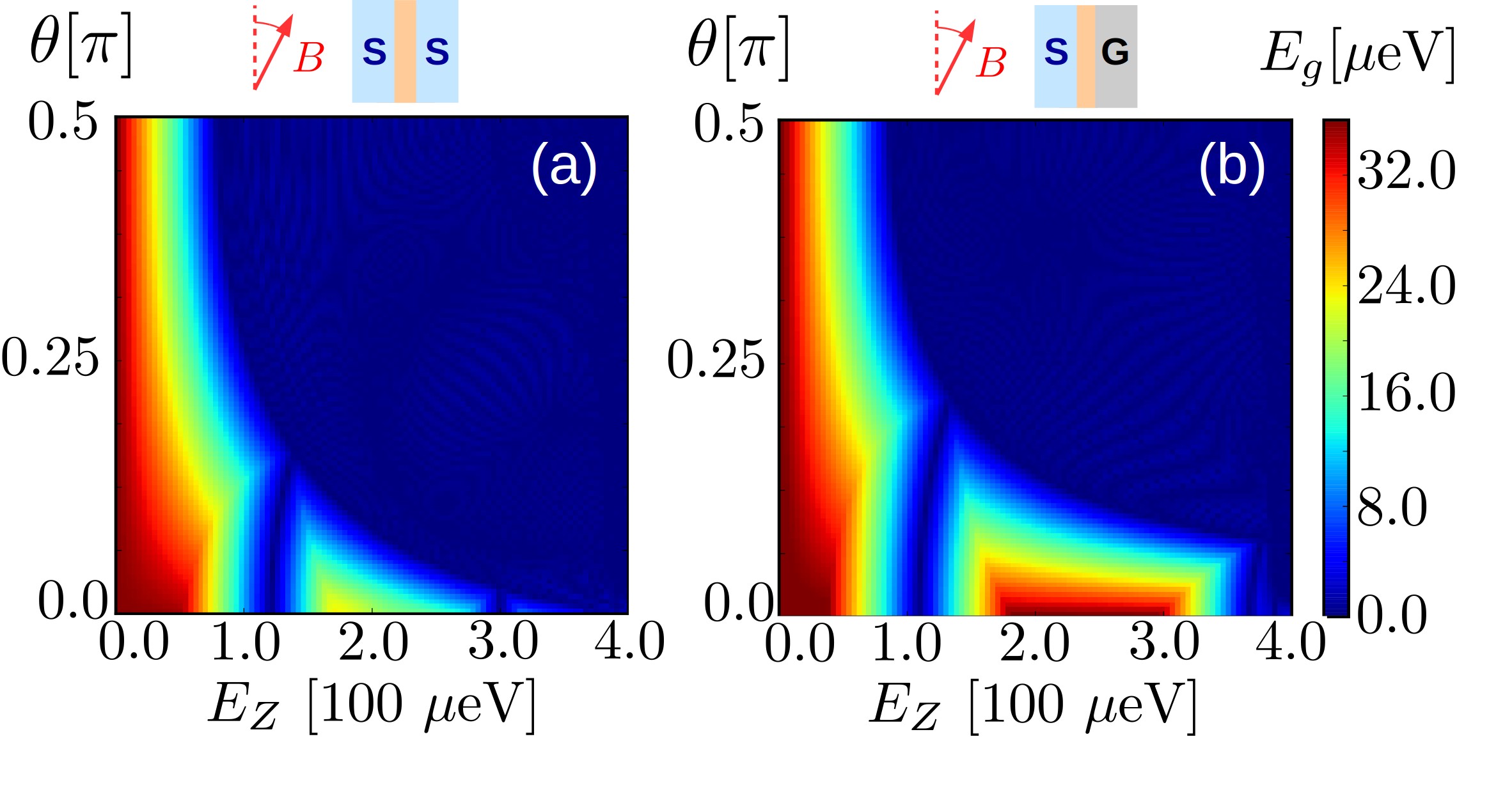
We find that the topological gap is suppressed when the magnetic field is rotated away from the stripe direction [Fig. S5]. For a symmetric device structure, the topological regime breaks down for an angle of about close to the first phase-transition point and for even smaller angles when the Zeeman energy approaches the second phase-transition point [Fig. S5(a)]. By contrast, the topological regime is more stable against rotations of the magnetic-field direction for an asymmetric device design: Here, the topological regime persists up to . Hence, an asymmetrically gated structure is also favorable to stabilize the MBS against a misalignment of the magnetic field.
Irrespective of the design, we conclude, however, that a network of MBS in a 2DEG structure should contain all Majorana stripes in parallel. This is an important restriction for the device design that we accounted for in our device suggestions in Fig. 4 in the main part.