Intelligent Pinning Based Cooperative Secondary Control of Distributed Generators for Microgrid in Islanding Operation Mode
Abstract
Motivated by the fact that the location(s) and structural properties of the pinning node(s) affect the algebraic connectivity of a network with respect to the reference value and thereby, its dynamic performance, this paper studies the application of intelligent single and multiple pinning of distributed cooperative secondary control of distributed generators (DGs) in islanded microgrid operation. It is shown that the intelligent selection of a pinning set based on the degree of connectivity and distance of leader DG(s) from the rest of the network improves the transient performance for microgrid voltage and frequency regulation. The efficacy of the distributed control strategy based on the proposed algorithms is illustrated via numerical results simulating typical scenarios for a variety of microgrid configurations.
I Introduction
Voltage and frequency regulation of microgrid are essential in both grid connected and islanded modes [1, 2, 3]. In grid connected mode, frequency is dictated by the main grid while the voltage within the microgrid can be regulated based on its reactive power generation and consumption. When the microgrid disconnects from the main grid in response to, say, upstream disturbance or voltage fluctuation and goes to islanding mode, both voltage and frequency at all locations in the microgrid have to be regulated to nominal values. Typical microgrid control hierarchy includes (1) primary control for real and reactive power sharing between distributed generators (DGs) [4, 5, 6, 7]; and (2) secondary control to maintain load voltage and frequency close to nominal values via respective references communicated to each DG [3][8] from a controller. Using centralized control requires complex and expensive communication infrastructure and is subject to failure in the central controller and communication links. To overcome these limitations, distributed cooperative control [9, 10, 11] can be utilized which employs a sparse network. The application of cooperative control for DG operation in power systems in grid connected mode has been studied in [11, 12, 13, 14] among others. The technique of providing the reference values to only a fraction of the DGs in the network, known as pinning, has been studied in [15][16]. In [17], pinning control in microgrid islanding mode using energy storage system as master unit was recently studied. In [18], Bidram et al. employed multi-agent distributed cooperative secondary voltage control of the microgrid.
In the aforementioned studies, the selection of the pinned (or leader) DG(s) has been assumed to be arbitrary. However, as has been shown in [19, 20, 21], the performance and robustness of the network is directly related to the choice of the pinning set, i.e., the set of pinned or leader DG(s). Recent results obtained by the authors in [22] obtain tight upper and lower bounds on the algebraic connectivity of the network to the reference signal111Algebraic connectivity to the reference signal [20] is a measure of the availability of the reference information in the overall network.. By taking advantage of these novel results, the work in this paper proffers multiple novel contributions. We first formulate the problem of single and multiple pinning of multi-agent distributed cooperative control in microgrids. Next, the effect of proper selection of pinning DGs is discussed. Then, we propose two implementable pinning node(s) selection algorithms based on degree and distance of the candidate leader(s) from the rest of the microgrid. Several cases of power system topologies and communication networks as well as different scenarios are numerically simulated to show that intelligent selection of the pinning node(s) results in better transient performance of the DGs’ terminal profiles.
The remainder of the paper is organized as follows. Section II reviews the microgrid primary and secondary control schemes for regulating voltage and frequency. The intelligent single and multiple pinning problems are formulated in Section III followed in Section IV by a presentation of the algorithms for solving these problems. Section V illustrates the performance of the proposed algorithms via extensive numerical simulation studies while section VI concludes the paper.
II Microgrid System Model
In this section, we briefly describe the basic system model consisting of the inverter based DG, the primary controller for the DG, and the distributed cooperative secondary controller. For more details, the reader is referred to the development in [18][23] and the references therein.
II-A DG Model and Primary Control
The inverter based DG model consists of a three legged inverter bridge connected to a DC voltage source. The DC bus dynamics and switching process of the inverter can be neglected due to the assumptions of an ideal DC source and realization of high switching frequency of the bridge, respectively. The output frequency and voltage magnitude of each DG are set in accordance with the droop controllers [5]. The output voltage magnitude and frequency control of the inverter itself is typically implemented with internal current controllers in the standard rotating reference frame with the d-axis aligned to the output voltage vector, e.g., see [24]. From the droop control point of view, the inverter can be assumed to be ideal in the sense that its output voltage magnitude and frequency are regulated to the desired values of and , respectively, within the time frame of interest. Thus,
| (1) |
where and are the desired angular frequency and voltage amplitude of the DG, respectively; and are the active and reactive power outputs of the DG; and are reference angular frequency and voltage set points determined by the secondary control, respectively; and and are droop coefficients for real and reactive power. Here, and are generated by passing the instantaneous real and reactive power outputs of the inverter through first order low pass filter with corner frequency to eliminate undesired harmonics
| (2) |
II-B Distributed Cooperative Secondary Control
II-B1 Secondary Voltage and Frequency Control
The goal in secondary voltage control is to determine the primary control reference voltage inside each DG so as to minimize the deviation of the concerned DG’s output voltage from the constant nominal reference voltage . Mathematically, this is accomplished by the following set of equations
| (3) |
where is an auxiliary control input given by
| (4) |
where is the voltage regulation error for DG , is a control gain, while denote the total number of DGs in the network. Here, is the adjacency matrix of the communication network, indicates a connection from DG to DG and otherwise ; is the pinning gain of the DG and indicates which nodes are pinned to the reference value.
For the secondary frequency control, the twin objectives are to ensure that the frequency of each DG reaches the reference frequency while at the same time ensuring that active power is shared in proportion to the rating of the individual DGs. In other words, leader-following consensus and leaderless consensus problems are solved as follows
| (5) |
where is the first of two auxiliary control inputs given by
where is the control gain and is the frequency regulation error of the DG with respect to the reference signal. The second auxiliary control term (added to ensure that generators share active power in accordance with their ratings as captured in the droop curve coefficients ) is generated as follows
| (6) |
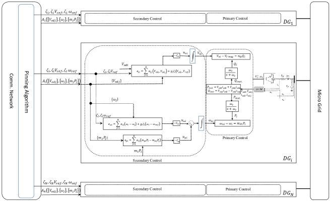
where is a control gain. A block schematic of the microgrid with voltage source inverter (VSI) based DGs alongside the primary and secondary controllers is shown in Fig. 1.
II-B2 Error Dynamics
After substituting (4) and (5) into the time dynamics of (1), we have
| (7) | |||||
| (8) |
where and denote the output voltage and frequency regulation errors of the network, is the network’s pinning gain matrix, is the pinning matrix, and is the Laplacian of the adjacency matrix defined as
| (9) |
From (7) and (8), it is clear that pinning choices and are critical to the performance of the secondary controller.
III Pinning Problem
III-A Problem Formulation
As is well known from linear time-invariant system theory, the performance and robustness of the systems in (7) and (8) are directly dependent on the eigenvalues of . Therefore, choosing which DG(s) to provide the reference values to, i.e., , has an enormous impact on the performance of the microgrid. The first problem (Pinning Problem 1) that is addressed in this paper is that of choosing the location of the nodes to be pinned under the specification of a given size of the pinning set. In other words, given a desired number of desired pinning nodes , one needs to determine the that maximizes the minimum eigenvalue of the closed-loop system. The second problem (Pinning Problem 2) addressed in this paper is to find the minimum number of pinning nodes (and their locations) while guaranteeing a certain specified convergence rate .
III-B Solutions to the Pinning Problems
It is well known that the optimal solutions for the aforementioned problems have exponential complexity [25]. Thus, finding the optimal solution is not practical in microgrids with large number of DGs which renders suboptimal solutions with polynomial time complexity to be of immense interest [22, 19, 20, 21]. To develop any effective algorithm for either of the pinning problems stated above, we need to understand how the structural properties (such as distance, number of connections, etc.) of the pinning set in the network affects the algebraic connectivity, , of the network with respect to the reference. One possible way to understand these effects is by utilizing lower and upper bounds on . A set of tight upper and lower bounds on the algebraic connectivity of the network with respect to the reference have recently been developed in [22] and are provided in Appendix A for the case of pinned nodes with . In what follows, we discuss the implications of these bounds.
For illustration, consider first the single pinning case where the reference value is only available in one DG (i.e., ). Based on the bounds in Appendix A, it is clear that the upper bound on is a strictly increasing function of the degree of the pinning node and its pinning gain . Additionally, if the pinning gain, , is considered to be very large, the upper bound on algebraic connectivity of the network with respect to the reference can be shown to be bounded as where denotes the out degree of the pinning node. Since , the algebraic connectivity of the network with respect to the reference cannot exceed for the single pinning case. Thus, it is clear to see that the convergence rate of the errors in (7) and (8) cannot exceed and for voltage and frequency, respectively. Since we established that the algebraic connectivity of the network with respect to the reference is upper bounded by , it can be conjectured that pinning a DG with higher out-degree is more effective than pinning a DG with lower out-degree. Furthermore, from the given lower bound on in Appendix A, it can be concluded that another topological characteristic to choose the pinning DG is its centrality value which is a measure of its distance from the farthest DG in the network. This means that the candidate DG for pinning should have a low distance from the rest of the network. The general case of multiple pinning (i.e., ) can be understood by considering the set of pinned DGs as a supernode in the network and by calculating all the topological properties according to this modified definition.
Before we proceed to state the algorithms arising from these bounds, let us state the following nomenclature
| length of shortest path from DG to | ||||
| DG , | ||||
where is the set of all DGs, denotes the pinning set, where denotes minus operation for sets, while d is the number of links directed from the pinning DGs to the rest of the network.
III-B1 Suboptimal Algorithm for Pinning Problem 1
This algorithm will choose pinning DGs to maximize the minimum eigenvalue of the closed-loop system. Since the upper bound on the minimum eigenvalue of the pinned network is an increasing function of the degree of the pinning DG, the DGs are sorted by decreasing degree; furthermore, from (14), we know that the minimum path length between the pinning set and the rest of the network should be minimized. Hence, the added pinning DG to the pinning set should maximize the combined measure, which is the minimum path length between the candidate pinning DG and the rest of the network subtracted from the out-degree of pinning. This procedure should continue until there DGs in the pinning set. The pseudo-code of this algorithm can be given as
Algorithm 1.
-
1.
and ,
-
2.
while do
-
•
d
-
•
, .
-
•
III-B2 Suboptimal Algorithm for Pinning Problem 2
In the second problem, let be the desired algebraic connectivity of the network to the reference. Since the algebraic connectivity of the network to the reference cannot exceed the maximum out-degree of the pinning set, the minimum number of pinning DGs to achieve a target convergence rate is given as . Consequently, the smallest number of pinning DGs, , to achieve the desired convergence rate should be chosen such that summation of the highest degree DGs should exceed . Algorithm 1 is started with this and arrives at a pinning set . If the condition is satisfied, the algorithm stops, otherwise, one more pinning DG is added using Algorithm 1 until the desired convergence rate is achieved. The pseudo-code of this algorithm can be expressed as
Algorithm 2.
-
1.
Sort the degree of the DGs such that
-
2.
Set to be smallest integer such that
-
3.
and ,
-
4.
while do
-
(a)
-
(b)
, .
-
(a)
-
5.
if , then stop;
else: set and go to 4.
IV Numerical Results
IV-A Grid and Controller Parameters
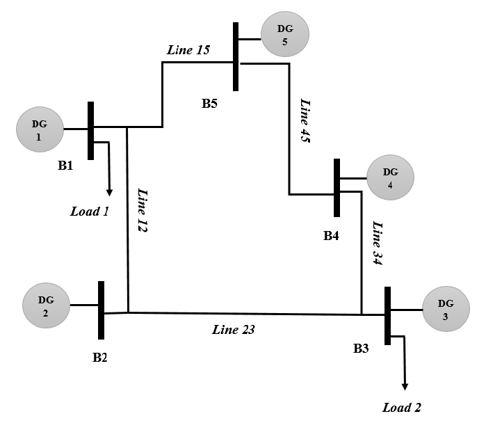
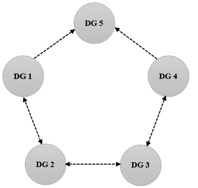

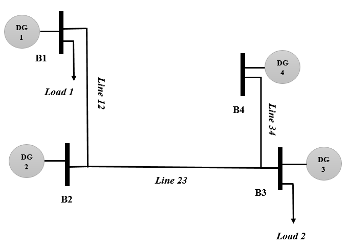
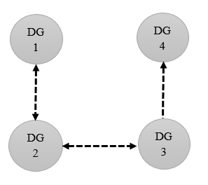
For our numerical simulations, we have used the Simpower System Toolbox of Simulinkfor 4 bus and 5 bus power systems, shown in Figs. 2 and 3, with different topologies and communication networks to show the adaptability and effectiveness of the proposed pinning control method. Microgrid operates on a 3-phase, 380V(L-L) and frequency of 50 Hz (). Unequal parameters of the DGs are given in the top section of Table I while the remaining parameters are adopted from [24]. In all case studies, DG 3 and DG 4 are assumed to be Type II DGs and the rest of the DGs are considered to be Type I. Loads are as given in the bottom section of Table I.
As mentioned earlier, an ideal DC source is assumed from DG side, therefore, the weather effect is not considered in this study. The cut-off frequency of the low-pass filters, , is set to . The control gains , and are all set to . It should be noted that microgrid islanding operation is detected based on the status of the main breaker and disconnect switches at utility/grid point of connection. We note here that the undershoot/overshoot of voltage amplitude and frequency of the DGs in microgrid during the transient from grid connected to islanding mode should not exceed 10-20 cycles to avoid the operation of 27, 59, and 81 protective relays. Generally, the protective power relays for voltage and frequency are typically set to and for 10-20 cycles. The microgrid’s main breaker opens at and goes to islanding mode at which time the secondary voltage and frequency control are activated.
As shown in Figs. 2 and 3, our study cases will illustrate both two-way (undirected) and one-way (directed) communication links in the microgrid. In one-way communication links, we restrict the transition function so that the new state of the sender does not depend on the current state of the receiver (a neighboring DG). Security of the location of a DG and the criticality of the load that it feeds are factors to be considered when deciding on directed vs undirected communication links.
IV-B Case 1: Pinning to Ensure Prescribed Convergence Rate
|
|||||||||
|
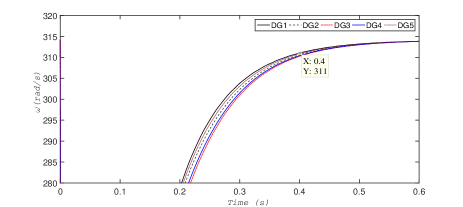
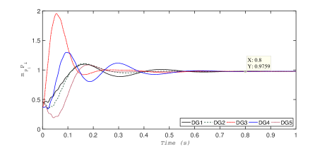
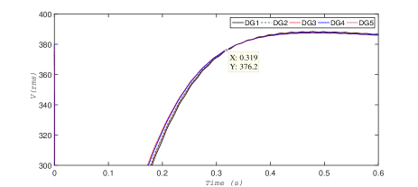
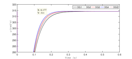
Let the pinning gain be and the desired convergence rate be . From the formulation of Problem 2, we can find the desired algebraic connectivity to the reference to be for voltage222Since and are chosen the same, this calculation holds for frequency as well.. Running Algorithm 2 gives two single pinning solutions, viz., or ; in the first iteration of step 4, we have , , and . Since out degree of both DG2 and DG3 are the same, the algorithm predicts that the performance for pinning either one of these DGs should be identical. As determined by the algorithm, pinning DG5 will not help microgrid synchronization because it does not share any information with any of its neighboring DGs. Fig. 5 shows the results for this case. The exponential convergence rate can be calculated as and for frequency and voltage, respectively. The output powers of the DGs for pinning of DG3 are shown in Fig. 5 to illustrate proper power sharing during islanded operation of the microgrid.
Now, if the desired convergence rate is set to , we find the required algebraic connectivity to be . Algorithm 2 results in a solution pinning two DGs (), viz., : in the first iteration, as before, either DG2 or DG3 should be selected. If DG2 is selected at the start of the second iteration, we have and and . Therefore, for the pinning is . If in the first iteration, DG3 is selected, then and the pinning set , which also predicts that the performance of pinning is the same as pinning . This can be deduced from the symmetry in the network. The results of numerical simulations with this choice are given in Fig. 6. The respective convergence rates for voltage and frequency in this case can be computed to be and , respectively.
IV-C Case 2: Load Variation
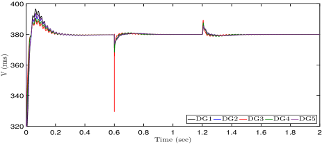
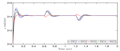
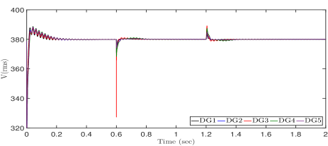
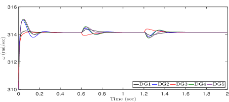
In Fig. 8, a severe scenario for load variation of the microgrid in Fig. 3 is considered to show the effectiveness of our proposed intelligent single and multiple pinning algorithms. As was mentioned earlier, our proposed algorithm chose DG3 for a single pinning solution and selected pinning sets or ) for a multiple pinning solution. In the load variation scenario, the primary load on Bus 3 is fixed with power factor of ; then, another mostly active load of is added at 0.6 and removed at . As can be observed from the results shown in Figs. 7 and 8, our intelligent pinning algorithm based solutions are comparatively more robust under this load variation scenario and bring back the voltage and frequency of the microgrid to the reference value very fast. Results also indicate the superior performance of the multiple pinning algorithm in comparison with single pinning algorithm during load variation.
IV-D Case 3: Comparative Study
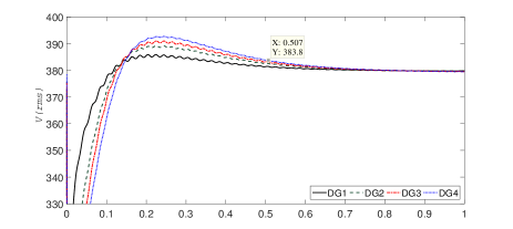
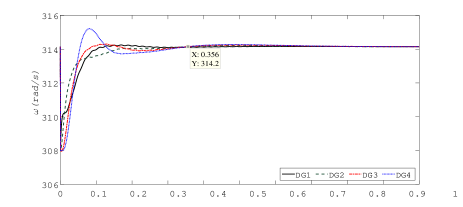
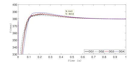
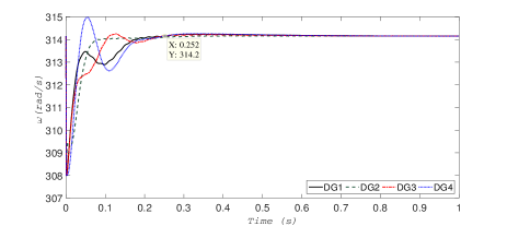
Here, we assume that the network is to be stabilized by single pinning method. The bus and communications networks are given in Fig. 2. In this configuration, it is assumed that the DGs communicate with each other through a fixed communication network shown in Fig. 2(b). The diagram shows that the DGs only communicate with their neighboring DG. The DGs’ terminal voltage amplitude and frequency for different reference single pinning scenario are shown in Fig. 9. Based on the tracking synchronization control strategy, it can be seen that all DGs’ terminal voltage and frequency return to the reference value dictated by the leader DG. However, pinning DG2 results in a faster and more robust convergence in comparison with DG1 presented in [18]. Please note that in [18], because of its minimum directed communication topology, pinning DG1 is suggested while our pinning algorithm indicates that DG2 should be pinned which also coincides with the optimal solution of Problem 1.
Table II provides information about settling time of DGs’ terminal voltage and frequency for different pinning cases. As can be observed in Fig. 9(b), pinning DG2 results in better transient behavior, compared to pinning the other DGs in the network. It should be noted that DG4 cannot be selected as a leader because it does not share information with the rest of the microgrid. This is also true for pinning DG5 in 5-bus power systems in Fig. 3.
| Pinning DG | |||
|---|---|---|---|
| DG1 | 0.51 | 0.36 | 6 |
| DG2 | 0.43 | 0.25 | 4 |
V Conclusions
Intelligent single and multiple pinning based distributed cooperative control algorithms have been proposed to efficiently synchronize DGs in a microgrid to their nominal voltage and frequency values after disconnecting from the main grid. It has been shown that selection of pinning nodes depends directly on the power system and communication network topologies. Case studies using different types of microgrid configurations and scenarios demonstrate that the proposed methodology helps the DGs in the microgrid achieve convergence with desired rate and improved transient voltage and frequency behavior after going to islanding mode.
References
- [1] A. Mehrizi-Sani and R. Iravani, “Potential-function based control of a microgrid in islanded and grid-connected models,” IEEE Trans. Power Syst., vol. 25, pp. 1883-1891, Nov. 2010.
- [2] Y. A. R. I. Mohamed and A. A. Radwan, “Hierarchical control system for robust microgrid operation and seamless mode transfer in active distribution systems,” IEEE Trans. Smart Grid, vol. 2, pp. 352-362, Jun. 2011.
- [3] A. Bidram and A. Davoudi, “Hierarchical structure of microgrids control system,” IEEE Trans. Smart Grid, 3(4), pp. 1963-1976, 2012.
- [4] K. D. Brabandere, B. Bolsens, J. V. den Keybus, A. Woyte, J. Driesen, and R. Belmans, “A voltage and frequency droop control method for parallel inverters,” IEEE Transactions on Power Electronics, vol. 22, pp. 1107-1115, 2007.
- [5] M. Chandorkar and D. Divan, “Decentralized operation of distributed ups systems,” in Proc. IEEE PEDES, pp. 565-571, 1996.
- [6] M. Prodanovic and T. Green, “High-quality power generation through distributed control of a power park microgrid,” IEEE Transactions on Power Delivery, vol. 53, pp. 1471-1482, 2006.
- [7] M. N. Marwali, J.-W. Jung, and A. Keyhani, “Control of distributed generation systems part II: load sharing control,” IEEE Transactions on Power Electronics, vol. 19, pp. 1551-1561, 2004.
- [8] D. E. Olivares et al., “Trends in microgrid control,” in IEEE Trans. Smart Grid, vol. 5, no. 4, pp. 1905-1919, July 2014.
- [9] Ren, W., Beard, R.W., Distributed consensus in multi-vehicle cooperative control: theory and applications, Springer, London, 2009.
- [10] R. Olfati-Saber, J. Fax, and R. M. Murray, “Consensus and cooperation in networked multi-agent systems,” Proceedings of the IEEE, vol. 95, pp. 215-233, Jan. 2007.
- [11] Xin, H., Qu, Z., Seuss, J., Maknouninejad, “A self-organizing strategy for power flow control of photovoltaic generators in a distribution network,” IEEE Trans. Power Syst. , 26, pp. 1462-1473, 2011.
- [12] J. W. Simpson-Porco, F. Dörfler, and F. Bullo, “Synchronization and power sharing for droop-controlled inverters in islanded microgrids,” Automatica, vol. 49, no. 9, pp. 2603-2611, Sep. 2013.
- [13] L. Y. Lu and C. C. Chu, “Autonomous power management and load sharing in isolated micro-grids by consensus-based droop control of power converters,” Future Energy Electronics Conference (IFEEC), pp.365-370, Nov. 2013.
- [14] J. Y. Kim, J. H. Jeon, S. K. Kim, C. Cho, J. H. Park, H. M. Kim, and K. Y. Nam, “Cooperative control strategy of energy storage system and microsources for stabilizing the microgrid during islanded operation,” IEEE Transactions on Power Electronics, vol. 25, no. 12, pp. 3037-3048, Dec. 2010.
- [15] H. Su, Z. Rong, M. Z. Q. Chen, X. Wang, G. Chen, and H. Wang, “Decentralized adaptive pinning control for cluster synchronization of complex dynamical networks,” IEEE Trans. Cybernet., vol. 43, no. 1, pp. 394-399, Feb. 2013.
- [16] X. Li, X. F. Wang, and G. R. Chen, “Pinning a complex dynamical network to its equilibrium,” IEEE Trans. Circuits Syst. I, Reg. Papers, vol. 5, no. 10, pp. 2074-2087, Oct. 2004.
- [17] W. Liu, W. Giu, W. Sheng, X. Meng, Sh. Xue, and M. Chen, “Pinning-based distributed cooperative control for autonomous microgrids under uncertain communication topologies,” IEEE Trans. Power Syst., vol. 31, no. 2, pp. 1320-1329, Mar. 2016.
- [18] A. Bidram, A. Davoudi, F. L. Lewis, and J. M. Guerrero, “Distributed cooperative secondary control of microgrids using feedback linearization,” IEEE Trans. Power Syst., vol. 28, no. 3, pp.3462-3470.
- [19] S. Manaffam and A. Seyedi, “Pinning control for complex networks of linearly coupled oscillators,” in American Control Conference (ACC) , 2013 , vol., no., pp. 6364-6369, June 2013.
- [20] P. DeLellis, M. Di Bernardo, and F. Garofalo, “Adaptive pinning control of networks of circuits and systems in Lur’e form,” IEEE Trans. Circuits Syst. I, Reg. Papers, vol. 60, pp. 1-10, 2013.
- [21] T. Chen, X. Liu, and W. Lu, “Pinning complex networks by a single controller,” IEEE Trans. Circuits Syst. I, vol. 54, no. 6, pp. 1317-1326, Jun. 2007.
- [22] S. Manaffam, M. Talebi, A. Jain, and A Behal, “Synchronization in networks of identical systems via pinning: application to distributed secondary control of microgrids,” IEEE Transactions on Control Systems Technology, under review, available at https://arxiv.org/abs/1603.08844.
- [23] A. Bidram, A. Davoudi, F. L. Lewis, and Z. Qu, “Secondary control of microgrids based on distributed cooperative control of multi-agent systems,” IET Gener. Transm. Distrib., vol. 7, no. 8, pp. 822-831, Aug. 2013.
- [24] N. Pogaku, M. Prodanovic, and T. C. Green, “Modeling, analysis and testing of autonomous operation of an inverter-based microgrid,” IEEE Trans. Power Electron., vol. 22, no. 2, pp. 613-625, Mar. 2007.
- [25] W. Yu, G. Chen, and J. Lu, “On pinning synchronization of complex dynamical networks,” Automatica, vol. 45, no. 2, pp. 429-435, 2009.
- [26] H. A. Palizban and H. Farhangi, “Low voltage distribution substation integration in smart microgrid, ” presented at the 2011 IEEE 8th International Conference on Power Electronics and ECCE Asia, pp. 1801-1808, May-June 2011.
- [27] V. Kounev, D. Tipper, A. A. Yavuz, B. M. Grainger, and G. Reed, “A secure communication architecture for distributed microgrid control,” IEEE Transactions on Smart Grid, vol. 6, no. 5, September 2015.
Appendix A Bounds on
Let us assume that the nodes are pinned, this is called the pinning set. Let the farthest node to pinning set, , be . Then, define the set as
| (10) |
where are entries of the adjacency matrix of the communication network, , and denotes minus operation for sets. For each set in (10), we define the following
| (11) | ||||
| (12) |
where . Please note that due to the definition in (10), . From Theorem 3 in [22, Theorem 2], given an undirected network (i.e., information can flow both ways) with pinning set, , and , the algebraic connectivity of the network can be bounded as follows
where the upper bound
| (13) |
with
while the lower bound, , is the smallest positive root of the polynomials,
| (14) |
where
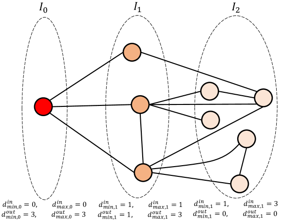
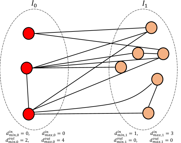
Figs. 11 and 11, respectively, illustrate the sets and variables defined above for sample single () and multiple () pinning cases.
