An ab initio investigation of Bi2Se3 topological
insulator
deposited on amorphous SiO2
Abstract
We use first-principles simulations to investigate the topological properties of Bi2Se3 thin films deposited on amorphous SiO2, Bi2Se3/a-SiO2, which is a promising substrate for topological insulator (TI) based device applications. The Bi2Se3 films are bonded to a-SiO2 mediated by van der Waals interactions. Upon interaction with the substrate, the Bi2Se3 topological surface and interface states remain present, however the degeneracy between the Dirac-like cones is broken. The energy separation between the two Dirac-like cones increases with the number of Bi2Se3 quintuple layers (QLs) deposited on the substrate. Such a degeneracy breaking is caused by (i) charge transfer from the TI to the substrate and charge redistribution along the Bi2Se3 QLs, and (ii) by deformation of the QL in contact with the a-SiO2 substrate. We also investigate the role played by oxygen vacancies () on the a-SiO2, which increases the energy splitting between the two Dirac-like cones. Finally, by mapping the electronic structure of Bi2Se3/a-SiO2, we found that the a-SiO2 surface states, even upon the presence of , play a minor role on gating the electronic transport properties of Bi2Se3.
I Introduction
Three-dimensional (3D) topological insulators (TIs) are a recently discovered class of materials and have attracted great attention due to their unique properties. They are insulators in the bulk phase but present topologically protected metallic states at the surface or interface with a trivial insulator Hasan and Kane (2010). The topological surface states (TSSs) or interface states (TISs) are spin-polarized Dirac fermion states, protected by time-reversal symmetry, and in the absence of magnetic impurities these states are insensitive to backscattering processes induced by time-reversal invariant impurities or defects Hasan and Kane (2010); Wray et al. (2011); Chen et al. (2010); Xu et al. (2012); Abdalla et al. (2013); Schmidt et al. (2011). These properties make TI materials suitable for spintronics applications Pesin and MacDonald (2012). In particular, Bi2Se3 is one of the most investigated 3D-TI, it has a rhombohedral structure composed by quintuple layers (QLs) of Se and Bi convalently bonded, and these QLs are stacked along the -axis by van der Waals (vdW) interactions Zhang et al. (2009); Xia et al. (2009); Hsieh et al. (2009).
To take advantage of TIs materials for technological applications is necessary that the topologically protected states remain intact upon interaction with other materials. Thus, the substrate choice for Bi2Se3 growth should be such that it preserves the TIs properties. Bi2Se3 has been grown on various substrates, e.g., graphene, Si(111), CaF2, CdS, Al22O3, SiO2, among others He et al. (2013). Amorphous phases of dieletric or insulator materials are widely used for electronic applications, and an interesting material often used for this purpose is the amorphous SiO2 (a-SiO2). Bi2Se3 thin films have been grown on a-SiO2 by different experimental technics Kong et al. (2010); Jerng et al. (2013), and it has recently been shown to present topologically protected surface states Steinberg et al. (2010); Bansal et al. (2014); Chang et al. (2015).
To better understand the interaction between Bi2Se3 thin films and the a-SiO2 substrate, we perform a first-principles investigation for increasing number of Bi2Se3 quintuple layers deposited on a-SiO2, (Bi2Se3)n/a-SiO2. We find that the Bi2Se3 layers are bonded to the a-SiO2 surface mediated by vdW interactions; where the lattice structure of the Bi2Se3 QLs are preserved. At the interface region we have found a net electronic charge transfer from the bottom-most Bi2Se3 QL to the a-SiO2 surface. There is a down-shift (up-shift) of the metallic TSSs (TISs), promoting electronic transport mediated by electrons (holes) on the surface (interface) Bi2Se3 QLs. We have also considered the presence of oxygen vacancies () on the surface, a-SiO2[], which is a quite common intrinsic defect. The strength of the Bi2Se3a-SiO2[] interaction is the same as that of Bi2Se3/a-SiO2, as well as the maintenance of the Bi2Se3 lattice structure. Further electronic structure calculations show that the a-SiO2 surface states, even upon the presence of , play a minor role on gating the electronic transport properties of Bi2Se3; where the defect level is resonant within the valence band of Bi2Se3, lying below the topologically protected metallic states.
II Computational details
The calculations are performed based on the density-functional theory (DFT), as implemented in the Vienna ab initio simulation package (VASP) Kresse and Furthmüller (1996). We use the generalized gradient approximation (GGA), in the form proposed by Perdew, Burke and Ernzerhof Perdew et al. (1996), to describe the exchange-correlation functional. The Kohn-Sham orbitals are expanded in a plane wave basis set with an energy cutoff of 400 eV. The electron-ion interactions are taken into account using the Projector Augmented Wave (PAW) method Kresse and Joubert (1999). The Brillouin Zone is sampled according to the Monkhorst-Pack method Monkhorst and Pack (1976), using at least a 221 mesh. We have also used a functional that accounts for dispersion effects, representing van der Waals (vdW) forces, according to the method developed by Tkatchenko-Scheffler (TS) Tkatchenko and Scheffler (2009), which is implemented on VASP Bucko et al. (2013). The inclusion of van der Waals forces in the simulations is necessary to obtain the correct vdW gap between consecutive QLs Lind et al. (2005), the interaction between the a-SiO2 substrate and Bi2Se3 is also better described with the inclusion of vdW interactions.
The amorphous structure was generated through ab initio molecular dynamics (MD) simulations based on the DFT approach as implemented in the VASP code. In Ref. Scopel et al. (2008), we present details on the generation procedure of amorphous SiO2 bulk structure. In order to generate the a-SiO2 surface, we have considered a a-SiO2 slab, where the boundary condition perpendicular to the surface plane (z direction) has been removed by introducing a vacuum region of 10 Å. The atomic positions have been relaxed until atomic forces were lower than 25 meV/Å.
III Results and Discussion
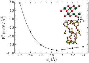
Our study starts by calculating the energetic stability and the equilibrium geometry of Bi2Se3 on the a-SiO2 substrate, Bi2Se3/a-SiO2. The binding energy () of Bi2Se3/a-SiO2 is defined as,
where and are the total energies of the separated components: a QL of Bi2Se3 and the a-SiO2 surface; and represents the total energy of the final system, a single QL of Bi2Se3 adsorbed on the a-SiO2 surface, as indicated in the inset of Fig. 1. Our results of , as a function of the vertical distance , are presented in Fig. 1. We find =–8.68 meV/Å2, for an (averaged) equilibrium distance of =2.90 Å. As observed for the QLs in the Bi2Se3 bulk, there is no chemical bonding between the Bi2Se3 and the a-SiO2 substrate, where the Bi2Se3a-SiO2 interaction is ruled by vdW forces. Similar picture has been verified for graphene on the a-SiO2 surface, where we found =6.3 eV/Å2,Miwa et al. (2011) which is in good agreement with the experimental estimative of Ishigami et al., 6 meV/Å2.Ishigami et al.
The absence of chemical bonding between the Bi2Se3 QL and the a-SiO2 surface has been maintained even upon the presence of oxygen vacancies () on the a-SiO2 surface (a-SiO2[]); is a quite common intrinsic defect in SiO2. We obtained practically the same values of binding energy, =–9.00 meV/Å2, and an equilibrium distance of 2.96 Å. For both systems, Bi2Se3/a-SiO2 and /a-SiO2[], the atomic displacements at the interface region are very small, preserving the lattice structure of Bi2Se3, supporting recent experimental results of scanning transmission electron microscopy.Bansal et al. (2014) Further comparisons indicate that, (i) the distance between the substrate and the Bi2Se3 QL is approximately 9% larger than the separation distance between consecutive QLs in the Bi2Se3 bulk phase,Lind et al. (2005); de Oliveira and Miwa (2016) and (ii) the Bi2Se3/a-SiO2 binding energy is about 40% lower (in absolute value) compared with the one between QLs in Bi2Se3 bulk phase. That is, the Bi2Se3Bi2Se3 interaction is stronger than that between Bi2Se3 and the a-SiO2 surface.
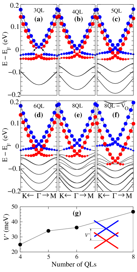
Next we investigate the electronic and topological properties of Bi2Se3/a-SiO2, as a function of the number of Bi2Se3 QLs () on the a-SiO2 surface, (Bi2Se3)n/a-SiO2. In (Bi2Se3)n/a-SiO2, the opposite sides of Bi2Se3 are in contact with different environments (with different dielectric constants), viz.: one (top-most) is in contact with a vacuum region, and the other (bottom-most) in contact with the a-SiO2 surface. There is no inversion symmetry in (Bi2Se3)n/a-SiO2, and thus the energy degeneracy between the edge (QL) states can be removed. Indeed this is what we verify in Fig. 2, where we present the electronic band structure of (Bi2Se3)n/a-SiO2 for =3, 4, 5, 6, and 8. The size of blue (red) circles (in Fig. 2) is proportional to the contribution of the Bi- orbitals of the bottom-(top-)most QL of the (Bi2Se3)n. We find that the surface states present an energy gap for =3 and 4, characterized by a Rashba-like band splitting near the point. Those Rashba-like energy bands present similar spatial distribution, and spin-texture (not shown) when compared with the ones observed for thin films of Bi2Se3 on SiC(0001) and InP(111).Zhang et al. (2010); Landolt et al. (2014) In addition, it is worth noting that electronic contributions from the edge QLs to the band apex, indicated by arrows near the point in Fig. 2(a), are reduced for =3 and 4. Those states are delocalized, spreading out along the Bi2Se3 layers, as verified for Bi2Se3 on InP(111). Landolt et al. (2014) Such a delocalization is supressed upon the formation of gapless Dirac bands for = 5, 6 and 8 [Figs.2(c)–2(e)], i.e. the topologically protected metallic bands become fully localized on the top-most surface, and bottom-most interface QLs of (Bi2Se3)n/a-SiO2.
As shown in Figs. 2(c)–2(e), the topological surface/interface states (TSSs/TSIs) move downward/upward with respect to the Fermi level. Those results suggest that there is a local -type (-type) doping of the edge QLs of Bi2Se3. Indeed, based on the Bader charge analysis method, Bader (1990) with the code developed by the Henkelman’s group,Henkelman et al. (2006) we find a net charge transfer from the bottom-most Bi2Se3 QL to the a-SiO2 surface atoms, giving rise to an electrostatic dipole at the interface region, as well as an electronic charge density rearrangement along the Bi2Se3 slab. In order to provide a measurement of the charge density imbalance along the Bi2Se3 layer, we compare the total charge densities at the edge QLs of (Bi2Se3)n/a-SiO2 with the ones of a free standing (Bi2Se3)n film. We find that the charge density reduces by 5.5–6.0 in the bottom-most QL, while it increases by 0.2–1.0 in the top-most QL. Thus, supporting the down-shift (up-shift) of the TSSs (TISs) lying on the surface (interface) QL of (Bi2Se3)n/a-SiO2.
The separation between the Dirac points [ in Fig. 2(g)] increases almost linearly with the number of QLs, even one QL before the closing of the energy gap, =4. Such a dependence of , with the width () of (Bi2Se3)n, can be attributed to the presence of a net electric field () along the (Bi2Se3)n film, .Yazyev et al. (2010) Where comes from the charge density imbalance discussed above, and the band bending due to the charge transfer at the (Bi2Se3)n/SiO2 interface. By changing the electronic structure at the Bi2Se3/a-SiO2 interface region, we may have different values of for a given (Bi2Se3)n width; for instance, the presence of oxygen vacancies on the a-SiO2 surface. As shown in Fig. 2(f), increases by 37 meV, =4784 meV in (Bi2Se3)8/a-SiO2[].
Tuning the electron chemical potential within the energy window given by , the energy separation between the opposite edge states of Bi2Se3/a-SiO2 will promote topologically protected electron (hole) currents on the top-most surface (bottom-most interface) states of Bi2Se3. In addition, the up-shift of the interface states in Bi2Se3/a-SiO2 indicates that the scattering rate between the TISs and the bulk continuum states will be reduced, while the TSSs will face an increase of such a scattering rate.Kim et al. (2011) Further control of the energy positions of those TSSs and TSIs can be done by an external electric field. Indeed, top-gate structures has been used to control the topological transport properties in thin films of Bi2Se3 on dielectric substrates.Steinberg et al. (2010); Ojeda-Aristizabal et al. (2012); Liu et al. (2015); Chang et al. (2015)
In Fig. 3(a), we present the energy positions of the isolated systems, valence band maximum (VBM) and the conduction band minimum (CBM) of pristine a-SiO2 (left), and defective a-SiO2[] (right) surfaces. Here, we have considered the vacuum level as the energy reference. The doubly occupied defect level (=–5.84 eV) lies at 1.46 eV above the valence band maximum.vac In the (Bi2Se3)8 film [Fig. 3(a) (center)], the Fermi level is given by the crossing on the TSSs; it lies in the energy gap of a-SiO2, and above the defect level () of a-SiO2[]. The position of the Fermi energy (), with respect to the vacuum level, corresponds to the work function () of free standing (Bi2Se3)8, =4.90 eV. Meanwhile, the work function of the final systems (), (Bi2Se3)8/a-SiO2 and /a-SiO2[], increases with respect to . Comparing those work functions, , we can infer the band bending of (Bi2Se3)8 upon the formation of the Bi2Se3/a-SiO2 interface.Khomyakov et al. (2009) We find positive values of , 0.30 and 0.21 eV for (Bi2Se3)8/a-SiO2 and /a-SiO2[], respectively, and thus supporting the electron transfer from Bi2Se3 to the a-SiO2 surface.
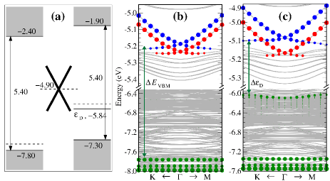
Aiming the development of electronic devices composed by thin films of Bi2Se3 with a-SiO2 as the dielectric gate, it is important to get a picture of the energy positions of the TSSs and TISs in Bi2Se3/a-SiO2. In Figs. 3(b) and 3(c) we present the electronic band structures of the final systems, (Bi2Se3)8/a-SiO2 and /a-SiO2[], respectively, including the orbital projection to the a-SiO2 surface. Those energy band diagrams show that (near the point) the TSSs and TISs states lie at about (i) 2.6 eV above the VBM of the a-SiO2 surface [ in Fig. 3(b)], and (ii) 0.9 eV above the defect level [ in Fig. 3(c)], which is resonant within the valence band of Bi2Se3. Thus, indicating that the electronic states of the a-SiO2 surface, even upon the presence of intrinsic defects like , will play a minor role on gating the electronic transport properties, mediated by the topological states, for Bi2Se3 films.
IV Conclusions
We have performed an ab initio investigation of Bi2Se3 topological insulator deposited on amorphous a-SiO2 substrate. The Bi2Se3 layers are bonded to the a-SiO2 surface through vdW interactions; preserving the lattice structure of the Bi2Se3 QLs. Topologically protected edge states are observed on the surface as well as at the interface layers of Bi2Se3, however they are no longer degenerated. The TSSs exhibit an energy-down-shift, followed by the up-shift of the TISs. The degeneracy break is caused by the combination of two effects: (i) charge transfer from the TI to the substrate and charge redistribution along the Bi2Se3 QLs, resulting in electron depletion (accumulation) at the closest (furthest) QL from the substrate; and (ii) the Bi2Se3 deformation due to the a-SiO2 interaction. Such an energy separation is increased by the presence of . Finally, by mapping the energy positions of the Bi2Se3 edge states, the VBM, CBM, and the defect level of a-SiO2, we verify that the a-SiO2 surface states will play a minor role on gating the electronic transport properties in Bi2Se3/a-SiO2 systems.
Acknowledgements.
This work was supported by the Brazilian Nanocarbon Institute of Science and Technology (INCT/Nanocarbono), and the Brazilian agencies CNPq, FAPES and FAPEMIG. The authors also acknowledge the computational support from CENAPAD/SP.References
- Hasan and Kane (2010) M. Z. Hasan and C. L. Kane, Rev. Mod. Phys. 82, 3045 (2010).
- Wray et al. (2011) L. A. Wray, S. Xu, Y. Xia, D. Hsieh, A. V. Fedorov, Y. S. Hor, R. J. Cava, A. Bansil, H. Lin, and M. Z. Hasan, Nat. Phys. 7, 32 (2011).
- Chen et al. (2010) Y. L. Chen, J. Chu, J. G. Analytis, Z. K. Liu, K. Igarashi, H. Kuo, X. L. Qi, S. K. Mo, R. G. Moore, D. H. Lu, M. Hashimoto, T. Sasagawa, S. C. Zhang, I. R. Fisher, Z. Hussain, and Z. X. Shen, Science 329, 659 (2010).
- Xu et al. (2012) S. Y. Xu, M. Neupane, C. Liu, D. Zhang, A. Richardella, L. A. Wray, N. Alidoust, M. Leandersson, T. Balasubramanian, J. Sánchez-Barriga, O. Rade, G. Landolt, B. Slomski, J. H. Dil, J. Osterwalder, T. R. Chang, H. T. Jeng, H. Lin, A. Basil, N. Samarth, and M. Z. Hasan, Nature Phys. 8, 616 (2012).
- Abdalla et al. (2013) L. B. Abdalla, L. Seixas, T. M. Schmidt, R. H. Miwa, and A. Fazzio, Phys. Rev. B 88, 045312 (2013).
- Schmidt et al. (2011) T. M. Schmidt, R. H. Miwa, and A. Fazzio, Phys. Rev. B 84, 245418 (2011).
- Pesin and MacDonald (2012) D. Pesin and H. MacDonald, Nature Materials 11, 409 (2012).
- Zhang et al. (2009) H. Zhang, C. X. Liu, X. L. Qi, X. Dai, Z. Fang, and S. C. Zhang, Nature Phys. 5, 438 (2009).
- Xia et al. (2009) Y. Xia, D. Qian, D. Hsieh, L. Wray, A. Pal, H. Lin, A. Bansil, D. Grauer, Y. S. Hor, R. J. Cava, and M. Z. Hasan, Nature Phys. 5, 398 (2009).
- Hsieh et al. (2009) D. Hsieh, Y. Xia, D. Qian, L. Wray, J. H. Dil, F. Meier, J. Osterwalder, L. Patthey, J. G. Checkelsky, N. P. Ong, A. V. Fedorov, H. Lin, A. Bansil, D. Grauer, Y. S. Hor, R. J. Cava, and M. Z. Hasan, Nature Lett. 460, 1101 (2009).
- He et al. (2013) L. He, X. Kou, and K. L. Wang, physica status solidi (RRL) 7, 50 (2013).
- Kong et al. (2010) D. Kong, W. Dang, J. J. Cha, H. Li, S. Meister, H. Peng, Z. Liu, and Y. Cui, Nano Letters 10, 2245 (2010).
- Jerng et al. (2013) S.-K. Jerng, K. Joo, Y. Kim, S.-M. Yoon, J. H. Lee, M. Kim, J. S. Kim, E. Yoon, S.-H. Chun, and Y. S. Kim, Nanoscale 5, 10618 (2013).
- Steinberg et al. (2010) H. Steinberg, D. R. Gardner, Y. S. Lee, and P. Jarillo-Herrero, Nano letters 10, 5032 (2010).
- Bansal et al. (2014) N. Bansal, N. Koirala, M. Brahlek, M.-G. Han, Y. Zhu, Y. Cao, J. Waugh, D. S. Dessau, and S. Oh, Applied Physics Letters 104, 241606 (2014).
- Chang et al. (2015) C.-Z. Chang, Z. Zhang, K. Li, X. Feng, J. Zhang, M. Guo, Y. Feng, J. Wang, L.-L. Wang, X.-C. Ma, et al., Nano letters 15, 1090 (2015).
- Kresse and Furthmüller (1996) G. Kresse and J. Furthmüller, Phys. Rev. B 54, 11169 (1996).
- Perdew et al. (1996) J. P. Perdew, K. Burke, and M. Ernzerhof, Phys. Rev. Lett. 77, 3865 (1996).
- Kresse and Joubert (1999) G. Kresse and D. Joubert, Phys. Rev. B 59, 1758 (1999).
- Monkhorst and Pack (1976) H. J. Monkhorst and J. D. Pack, Phys. Rev. B 13, 5188 (1976).
- Tkatchenko and Scheffler (2009) A. Tkatchenko and M. Scheffler, Phys. Rev. Lett. 102, 073005 (2009).
- Bucko et al. (2013) T. Bucko, S. Lebègue, J. Hafner, and Ángyán, Phys. Rev. B 87, 064110 (2013).
- Lind et al. (2005) H. Lind, S. Lidin, and U. Häussermann, Phys. Rev. B 72, 184101 (2005).
- Scopel et al. (2008) W. L. Scopel, A. J. da Silva, and A. Fazzio, Physical Review B 77, 172101 (2008).
- Miwa et al. (2011) R. Miwa, T. M. Schmidt, W. Scopel, and A. Fazzio, Applied Physics Letters 99, 163108 (2011).
- (26) M. Ishigami, J. H. Chen, W. G. Cullen, M. S. Fuhrer, and E. D. Williams, Nano Lett. 7, 1643.
- de Oliveira and Miwa (2016) I. S. S. de Oliveira and R. H. Miwa, Nanotechnology 27, 035704 (2016).
- Zhang et al. (2010) Y. Zhang, K. He, C. Chang, C. Song, L. Wang, X. Chen, J. Jia, Z. Fang, X. Dai, W. Shan, S. Shen, Q. Niu, X. Qi, S. Zhang, X. Ma, and Q. Xue, Nat. Phys. 6, 584 (2010).
- Landolt et al. (2014) G. Landolt, S. Schreyeck, S. V. Eremeev, B. Slomski, S. Muff, J. Osterwalder, E. V. Chulkov, C. Gould, G. Karczewski, K. Brunner, et al., Physical Review Letters 112, 057601 (2014).
- Bader (1990) R. F. W. Bader, Atoms in Molecules - A Quantum Theory (Oxford University Press, Oxford, 1990).
- Henkelman et al. (2006) G. Henkelman, A. Arnaldsson, and H. Jónsson, Comput. Mater. Sci. 36, 254 (2006).
- Yazyev et al. (2010) O. V. Yazyev, J. E. Moore, and S. G. Louie, Phys. Rev. Lett. 105, 266806 (2010).
- Kim et al. (2011) S. Kim, M. Ye, K. Kuroda, Y. Yamada, E. Krasovskii, E. Chulkov, K. Miyamoto, M. Nakatake, T. Okuda, Y. Ueda, et al., Physical Review Letters 107, 056803 (2011).
- Ojeda-Aristizabal et al. (2012) C. Ojeda-Aristizabal, M. Fuhrer, N. Butch, J. Paglione, and I. Appelbaum, Applied Physics Letters 101, 023102 (2012).
- Liu et al. (2015) Y. Liu, C. Chong, J. Jheng, S. Huang, J. Huang, Z. Li, H. Qiu, S. Huang, and V. Marchenkov, Applied Physics Letters 107, 012106 (2015).
- (36) By using the hybrid HSE06 approachJ. Heyd and Ernzerhof (2006) to the calculation of the exchange correlation energy, we find the doubly occupied defect level () at VBM+1.60 eV, where the VBM lies –8.30 eV below the vacuum level.
- Khomyakov et al. (2009) P. Khomyakov, G. Giovannetti, P. Rusu, G. v. Brocks, J. Van den Brink, and P. Kelly, Physical Review B 79, 195425 (2009).
- J. Heyd and Ernzerhof (2006) G. E. S. J. Heyd and M. Ernzerhof, J. Chem. Phys. 124, 219906 (2006).