Charged grain boundaries reduce the open-circuit voltage of polycrystalline solar cells–An analytical description
Abstract
Analytic expressions are presented for the dark current-voltage relation of a junction with positively charged columnar grain boundaries with high defect density. These expressions apply to non-depleted grains with sufficiently high bulk hole mobilities. The accuracy of the formulas is verified by direct comparison to numerical simulations. Numerical simulations further show that the dark can be used to determine the open-circuit potential of an illuminated junction for a given short-circuit current density . A precise relation between the grain boundary properties and is provided, advancing the understanding of the influence of grain boundaries on the efficiency of thin film polycrystalline photovoltaics like CdTe and .
I Introduction
Despite decades of research, the role of grain boundaries in the photovoltaic behavior of polycrystalline solar cells remains an open question Dharmadasa (2014); Kumar and Rao (2014). The high defect density of grain boundaries generally promotes recombination and reduces photovoltaic efficiency. However, thin film polycrystalline photovoltaics such as CdTe and exhibit high efficiencies despite a large density of grain boundaries Geisthardt, Topič, and Sites (2015); Topič, Geisthardt, and Sites (2015). The unexpected high efficiency of these materials demonstrates the need for a fuller understanding of grain boundary properties, and their influence on the charge current and recombination.
Numerous nanoscale measurements using electron beam induced current Yoon et al. (2013); Zywitzki et al. (2013); Li et al. (2014), scanning Kelvin probe microscopy Visoly-Fisher, Cohen, and Cahen (2003); Moutinho et al. (2010); Jiang et al. (2004a) and other techniques Tuteja et al. (2016); Sadewasser et al. (2011); Leite et al. (2014) have revealed that grain boundaries in these materials are positively charged (although previous work has also argued for negatively charged grain boundaries Galloway, Edwards, and Durose (1999)). Interpretation of these measurements is often challenging due to extraneous factors, such as surface effectsHaney et al. (2016). However, the information obtained from these measurements is sufficient to guide the construction of relevant models of grain boundaries. These models in turn provide critical feedback on the validity of the qualitative conclusions drawn from experiments.
The impact of charged grain boundaries on the photovoltaic efficiency has been studied using numerical simulations Gloeckler, Sites, and Metzger (2005); Taretto and Rau (2008); Rau, Taretto, and Siebentritt (2009); Troni et al. (2013), and to a lesser extent, analytic models Fossum and Lindholm (1980); Green (1996); Edmiston et al. (1996). These studies show that sufficiently large band bending at grain boundaries minimizes their impact on the short circuit current, but that grain boundaries always reduce the open-circuit voltage . This is consistent with the observation that the of CdTe is far below its theoretical maximum, and is the metric for which the largest efficiency improvements are availableGeisthardt, Topič, and Sites (2015). This highlights the need for a quantitative understanding of the impact of grain boundaries on . Although simulations can provide insight, the nonlinearities of the system and the large number of material parameters make it difficult to formulate a complete picture of the system using numerical modeling alone.
In this work we present analytical expressions for the dark current-voltage relation of a junction with positively charged, columnar grain boundaries. We find that grain boundaries contribute substantially to the dark current. Our analysis applies for grains which are not fully depleted and for materials with sufficiently high hole mobility. We show that the dark approximately determines and provides a closed form description for how charged grain boundaries reduce . Our analytical results follow from studying a large number of numerical simulations, formulating a physical picture of the electron and hole currents and recombination, and translating this picture into a simplified effective model which describes the essential features of the full simulation. We verify the accuracy of the simplified model by direct comparison with the simulations.
The paper is organized as follows: in Sec. II we describe the physical model and the assumptions we use in our analysis. In Sec. III we present the derivation of the dark relation. We find the system response depends qualitatively on the magnitude of the current: for lower currents, there is uniform recombination along the length of the grain boundary, while for higher currents, recombination is peaked at the grain boundary in the junction depletion region. The relations for these cases are summarized in Table 1. Similar results have been obtained in previous works on this problem Edmiston et al. (1996); Fossum and Lindholm (1980), however some of the relations we present are new. In Sec. IV we derive the bulk recombination current from the grain interior and junction depletion region. In Sec. V we show numerically that the dark yields a good estimate of . Finally we discuss the implications of our analysis for understanding how grain boundaries impact photovoltaic efficiency and measurements of these materials.
II Physical model of the grain boundary and restrictions
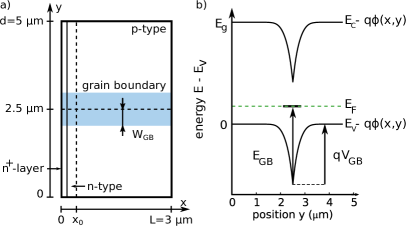
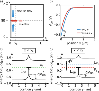
The model system, depicted in Fig. 1(a), is a junction of width and length with a single grain boundary perpendicular to the junction. We use selective contacts so that the hole (electron) current vanishes at (). We use periodic boundary conditions in the -direction so that the system constitutes an array of grain boundaries. The position within the depletion of the bulk junction at which plays a key role in our analysis, and is denoted by . Motivated by experimental evidence of charged grain boundaries as discussed in introduction, we consider a two-dimensional model of a positively charged grain boundary. The response of the system to this positive charge is to develop an electric field surrounding the grain boundary which attracts electrons and screens the grain boundary charge. This results in band bending around the grain boundary and the formation of a built-in potential across it, as seen in Fig. 1(b). Early measurements on CdTe bicrystals Thorpe, Fahrenbruch, and Bube (1986) showed built-in potentials ranging from to (in the dark) depending on sample preparation, while more recent studies Jiang et al. (2004b, 2013) on CdTe and thin films revealed barrier heights on the order of . While lower values of built-in potentials lead only to hole depletion at the grain boundary, larger barrier heights lead to type inversion at the grain boundary core (electrons become majority carriers). In this paper we consider positively charged grain boundaries in both inverted and non-inverted cases.
The grain boundary is readily modeled as a two-dimensional plane with an increased concentration of defect states. The grain boundary charge density from a single defect energy level reads Taretto and Rau (2008)
| (1) |
where is the 2D defect density of the grain boundary and is the absolute value of the electron charge. The occupancy of the defect level is given by Yang (1978)
| (2) |
where () is the electron (hole) density at the grain boundary, , are recombination velocity parameters for electrons and holes respectively, and and are
| (3) | ||||
| (4) |
where is the grain boundary defect energy level calculated from the valence band edge, () is the conduction (valence) band effective density of states, is the material bandgap, is the Boltzmann constant and is the temperature.
We consider large grain boundary defect densities, such that the Fermi level is pinned at (see Fig. 1(b)). In Appendix A we show that the density of defects required for Fermi level pinning must exceed , given by
| (5) |
For material parameters typical of CdTe, ranges from to for between and . Defining as the equilibrium potential difference between the grain boundary and bulk of the neutral -type region, then assuming leads to
| (6) |
We restrict our work to built-in potentials such that .
For nonequilibrium systems with unequal electron and hole quasi-Fermi levels, the assumption of the Fermi level pinning can be generalized in limiting cases. For , the grain boundary occupancy and charge is determined predominantly by , so that pinning of the Fermi level corresponds to pinning of the electron quasi-Fermi level to . Similarly, for , the hole quasi-Fermi level is pinned to . We will use the pinning of nonequilibrium quasi-Fermi levels in the analysis of dark grain boundary recombination in the next section.
The depletion region width surrounding the grain boundary in the -type region is as shown in Fig. 1(a) (the schematic neglects the modification of the grain boundary built-in potential in the junction depletion region). We restrict this work to grain sizes which are greater than , so that the grain is not fully depleted. For a doping density this requirement implies . As a point of comparison, recent cathodoluminescence spectrum imaging Moseley et al. (2015) shows that the average grain size in CdTe thin films (excluding twin boundaries) is .
Finally, we assume that the hole quasi-Fermi level is approximately flat across and along the grain boundary. In the analysis below we indicate precisely where this assumption is invoked, and provide a criterion for its validity. We find that for typical material parameters of CdTe, this assumption is generally valid.
III Grain boundary dark current
In this section we derive analytical expressions for the dark current originating from the grain boundary recombination. The general expression for the grain boundary recombination current density reads
| (7) |
where is the length of the grain boundary. is the recombination at the grain boundary and is of the Schockley-Read-Hall form
| (8) |
where is the intrinsic carrier concentration. , and are related to the electron and hole capture cross sections , of the grain boundary defect level by , where is the thermal velocity. In this work we vary ; for a fixed this corresponds to varying .
We begin with a descriptive overview of our main results. In all cases of interest, the grain boundary recombination current is of the general form
| (9) |
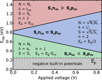
where is a surface recombination velocity, is a length characteristic of the physical regime, is an effective density of states, is an activation energy, is the applied voltage and is an ideality factor. The specific form of the parameters in Eq. (9) depends on the relative magnitudes of and . Fig. 2 shows the different regimes and how they depend on and , and the parameters for Eq. (9) in each case. We will refer to the case as an “-type” grain boundary, and the case as a “-type” grain boundary.
-type and -type grain boundaries share a number of similar characteristics. As discussed in Sec. II, for an -type (-type) grain boundary, the electron (hole) quasi-Fermi level is pinned to the grain boundary defect level, and the electrostatic potential along the grain boundary is approximately flat in both cases. As always, minority carriers control the recombination. For an -type grain boundary, recombination is determined by holes, which flow into the grain boundary from regions of the grain interior which are -type. This corresponds to positions (see Fig. 1(a)), and recombination at the grain boundary occurs uniformly throughout this region. For a -type grain boundary, recombination is determined by electrons, which flow into the grain boundary from the grain interior where (corresponding to ). The recombination also occurs at the grain boundary uniformly there. An asymmetry between -type and -type grain boundary recombination arises from the asymmetry of the bulk junction: most of the absorber layer is -type, so that .
For the case, the electrostatic potential along the grain boundary is no longer pinned to the grain boundary defect level, and is spatially varying. We find that the recombination also varies along the grain boundary and is peaked at a “hotspot” in the depletion region of the junction. The length scale over which recombination takes place is given by the electron’s effective diffusion length . This effective diffusion length is set by the grain boundary recombination velocity, and emerges from analyzing the one-dimensional motion of electrons electrostatically confined to the grain boundary core.
In the rest of this section we describe the physics of the three cases aforementioned and present equations for limiting conditions, leaving the general results and their derivations to the Appendices. While these limiting cases can sometimes be too restrictive, they provide accessible physical pictures that will allow the reader to quickly grasp the physics at play, and follow more easily the derivations presented in the Appendices. We support the physical descriptions with numerical simulation results for carrier densities along the grain boundary presented in Fig. 4. Comparisons of analytic derivations of electrostatic potential and electron quasi-Fermi level are presented in Fig. 10 in Appendix D.
III.1 Grain boundary recombination for
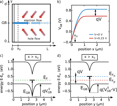
We first consider (-type grain boundary). As discussed in Sec. II, in this case the electron quasi-Fermi level is pinned to . In the -type grain interior, the applied voltage moves the minority carrier quasi-Fermi level away from the valence band by an amount (see Figs. 3(c) and (d)). We assume that is approximately flat across the grain boundary, so that everywhere in the bulk -type region, . Since is pinned to , the electrostatic potential of the grain boundary in the -region also varies with . The corresponding expression for in the -type region is then
| (10) | |||||
Equation (10) shows that the potential difference between grain boundary and neutral bulk decreases linearly with for . This is shown in Fig. 3(b). The physical picture is that the shift in leads to a nonequilibrium electron density in the absorber that accumulates at the grain boundary, partially neutralizing the positive charge there and reducing the electrostatic hole barrier surrounding the grain boundary. The reduction of this barrier results in a flow of holes towards the grain boundary, depicted schematically in Fig. 3(a). The holes recombine at the grain boundary core, generating an electron current which flows along the grain boundary, also shown in Fig. 3(a).
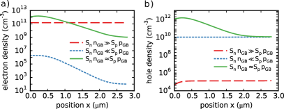
The uniform electron density along the grain boundary resulting from the pinning of the electron quasi-Fermi level to is shown in Fig. 4(a) (red dashed curve). Because is spatially uniform the electron current has only a drift component. The driving force for the drift current is an electrostatic potential that develops along the grain boundary. For low currents, the electrostatic field and associated electrostatic potential gradient is small and can be neglected. Using Eq. (10) and the assumption of flat hole quasi-Fermi level, Fig. 3(d) shows that the distance between and the valence band is ; the grain boundary hole density therefore reads
| (11) |
The hole density along the grain boundary is shown in Fig. 4(b) (red dashed curve). We note that the hole density slightly decreases at the -contact. However, this reduction is confined to the -region and is therefore negligible. Because the grain boundary recombination is determined by the hole density as shown in Fig. 4, and is given by
| (12) |
for . The recombination is uniform along the grain boundary, so the dark recombination current of Eq. (7) for voltages greater than simplifies to
| (13) |
The important features of Eq. (13) are: the saturation current varies as , the ideality factor is 1, and the thermal activation energy is .
III.2 Grain boundary recombination for
We now turn to the case (-type grain boundary). In this case the hole quasi-Fermi level is pinned to . In the -type bulk region, the applied voltage does not change the majority carrier quasi-Fermi level . Since is pinned to , the electrostatic potential of the grain boundary in the -region also does not change with . However, in the -type region (), the distance between and the conduction band increases by an amount , as shown in Figs. 5(c) and (d). The potential difference between grain boundary and grain interior decreases with there, shown in Fig. 5(b). This reduction in the grain boundary potential leads to an electron current flowing into the grain boundary for (see Fig. 5(a)), leading to recombination there. Assuming that is flat and equal to for (the electron current along the grain boundary being negligible there), Fig. 5(d) shows that the distance between and the conduction band is , resulting in on this section of the grain boundary.
This case requires a description of the electron transport at the grain boundary for . The electron density in this section of the grain boundary is the result of diffusion from the electrons accumulated at . The electrostatic potential transverse to the grain boundary confines electrons near the grain boundary core and leads to a one-dimensional motion along it. The length scale of the confinement is , where is the electric field transverse to the grain boundary in the neutral bulk of the junction. Grain boundary recombination results in an effective lifetime for confined electrons which satisfies , where is the bulk electron lifetime.
Upon integrating the continuity equation beyond (see Appendix C) the electron density along the grain boundary reads
| (15) |
where (: electron diffusion coefficient) is the diffusion length of electrons along the grain boundary. This diffusion length is derived from the electron effective lifetime given above. The behavior of the electron density as described by Eq. (15) is shown from the numerics in Fig. 4(a) (blue dotted curve). Because the recombination reads
| (16) |
for . From here we consider two limiting cases for the recombination current.
In the first limit, , electrons diffuse easily along the grain boundary. This case is obtained for small (possibly unphysical given the assumption of high ) values of recombination velocities. The limiting situation is a uniform electron density along the grain boundary, leading to the recombination current
| (17) |
The other limit is , where the electron density decays very rapidly for so that the recombination in dominates over the rest of the grain boundary. As a result, the recombination current reads
| (18) |
In this case electrons recombine close to the -contact before they can diffuse along the grain boundary. The electron density therefore transitions rapidly from to . The features of both regimes are analogous to : the saturation current varies as , the ideality factor is 1 and the thermal activation energy is .
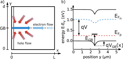
III.3 Grain boundary recombination for
As the applied voltage increases, the minority carrier density increases exponentially and approaches the majority carrier density. For applied voltages beyond this point, electroneutrality ensures that . Contrary to both previous cases, when , neither the electron nor hole quasi-Fermi level is pinned to , as shown by the bulk band structure in Fig. 6(b). To proceed in this regime, we consider the electron and hole currents along the grain boundary,
| (19) | ||||
| (20) |
where is the electrostatic potential along the grain boundary.
The assumption of flat hole quasi-Fermi level throughout the length of the grain boundary 111Because holes are majority carriers in the bulk of the absorber, the hole quasi-Fermi level is flat equal to there. We derived in Appendix B a criterion under which the hole quasi-Fermi level is flat across the grain boundary, so that the bulk quasi-Fermi level extends to the grain boundary core. means , which in turn implies equal and opposite hole drift and diffusion currents. Given , equal and opposite hole drift and diffusion currents implies equal electron drift and diffusion currents along the grain boundary. As in the case, the electrostatic potential transverse to the grain boundary confines the electron motion along the grain boundary core (we denote the confinement length by ), and the effective electron lifetime is again . Upon integrating the electron continuity equation in one dimension (see Appendix D), the electron and hole densities read
| (21) | ||||
| (22) |
where is the diffusion length of electrons along the grain boundary in this case. Carrier densities from numerical computation corresponding to this case are shown in Fig. 4 (green solid lines). Because , the recombination along the grain boundary is still given by Eq. (16), into which we insert Eq. (21) to obtain
| (23) |
for . Using the fact that , Eqs. (20) and (22) yield the electrostatic potential gradient along the grain boundary
| (24) |
Equation (24) corresponds to a spatially constant electric field along the grain boundary. We now consider two limiting cases for the recombination current by comparing to .
In the first limit, , Eq. (24) implies that the drop of electrostatic potential along the grain boundary is smaller than and is therefore negligible. The picture of a uniform grain boundary described in Sec. III.1, as well as the description of current flow given in Fig. 3(a) apply in this case. The recombination current is given by
| (25) |
Results similar to Eq. (25) are available in previous work Fossum and Lindholm (1980). The second limit, , occurs when the potential drop along the grain boundary is much greater than . In this case the recombination current reads
| (26) |
The physical picture associated with this case is shown in
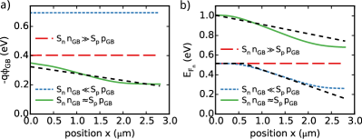
Fig. 6(a). Hole currents are directed toward the grain boundary in the junction depletion region, where holes recombine and generate an electron current mainly concentrated there. The recombination occurs primarily at this “hotspot” in the depletion region, in similar fashion (although with important differences) to previous studies of grain boundary recombination Green (1996). We refer to this case as the “hotspot” regime. In this limit, a strong electric field develops along the grain boundary to drive the electron flow. The corresponding steep drop in electrostatic potential, combined with the flat hole quasi-Fermi level suppresses the hole density and resulting recombination exponentially along the grain boundary. Fig. 4(b) (green solid curve) shows the suppression of the hole density away from the hotspot. In this case, the thermal activation energy is and the ideality factor is 2 (both typical of junction recombination). Previous experimental work which aimed to isolate the grain boundary recombination current in Si junctions observed such a thermal activation energy and ideality factor Neugroschel and Mazer (1982).
For , and , the system is in the hotspot regime for greater than . We again determine the conditions under which the assumption of a flat hole quasi-Fermi level is valid, which we quote here and derive in Appendix B
| (27) |
III.4 Numerical calculations
We perform numerical simulations of the drift-diffusion-Poisson equations for the geometry presented in Fig. 1(a) to test the accuracy of the above results. Table 2 gives the list of material parameters used for these calculations. We used infinite (zero) surface recombination velocities for majority (minority) carriers at the contacts, and periodic boundary conditions in the -direction.
In Fig. 7(a) the doping density is varied from to for . For the system is in the linear regime and the grain boundary recombination current is independent of as predicted by Eq. (13). Upon increasing above , the system switches to the hotspot regime given by Eq. (26), as can be seen by the change of slope of the current. This crossover is also shown in Fig. 2. The grain boundary recombination currents now depend on the doping density and do not overlap. The predicted scaling in is verified in the inset.
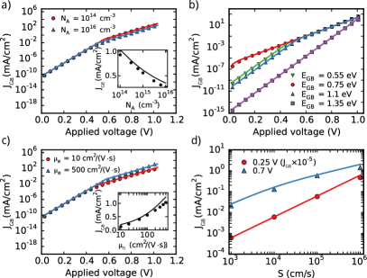
We show the dependence of the grain boundary recombination current on the defect energy level in Fig. 7(b). For applied voltages below , the grain boundary with remains in the linear regime , while for the grain boundary is always in the hotpot configuration as seen by the absence of slope change. The crossover between these regimes in the case confirms the independence of Eq. (26) of the grain boundary defect energy level. This is also seen for where one has a crossover between and . In addition, a comparison of the magnitudes of the recombination currents indicates that a higher defect energy level is favorable for reduced grain boundary recombination (a similar effect is obtained for low defect energy levels). This will impact the open-circuit voltage significantly, as will be discussed in Sec. V.
We vary the mobility of carriers (taken equal for electrons and holes) in Fig. 7(c) for . As predicted by Eq. (13) the linear regime is independent of mobility. The dependence of the hotspot regime on mobility is seen for , and we check the predicted square root scaling in inset. The grain boundary recombination current is increased as carrier mobility is increased. Increasing carrier mobility means that the gradient in electrostatic potential needed to drive the current along the grain boundary is reduced (see Eq. (24)). This in turn results in less suppression of hole density away from the hotspot, and an increase in the total grain boundary recombination. We also note that the electron mobility at the grain boundary controls the recombination. We have checked that changing the bulk electron mobility has no effect on the grain boundary recombination. A similar observation was made in Ref. Metzger and Gloeckler, 2005.
Our last test is in Fig. 7(d); we show grain boundary recombination currents in both regimes, and , as a function of surface recombination velocity. The analytical predictions are in good agreement with the numerical calculations, and we verify the dependence of the grain boundary recombination current for . This dependence only applies for ; for lower values of , the system crosses over between the hotspot and the linear configuration of the regime.
| Parameter | Value |
|---|---|
| to | |
| to | |
| to | |
Finally, we verified numerically that multiple parallel grain boundaries contribute independently to the recombination current. The total grain boundary recombination current is therefore the sum of individual grain boundary recombination currents, so that the formulas derived here can be readily applied to systems with non-uniform distribution of grain boundary properties.
IV Bulk recombination of the system
We now turn to the bulk recombination of the system. This comprises the recombination current from the junction depletion region, and the grain interior neutral and depletion regions.
The junction recombination current is taken from the standard 1D model of a junction Fonash (1981), and assumed uniform across the system
| (28) |
where is a fraction of the junction depletion region width.
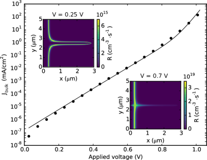
The behavior of the grain interior depletion region depends on the carrier densities at the grain boundary. In the regime of the -type grain boundary (), the majority carrier type of the grain boundary is inverted compared with the grain interior, which results in the crossing of the carrier densities in the grain interior depletion region. The recombination profile is therefore peaked with the same analytical expression as that of the junction depletion region. We suppose the recombination is uniform along the grain boundary, so that the integration along both sides of the grain boundary yields the recombination current
| (29) |
where is a fraction of the width of the grain interior depletion region surrounding the grain boundary. The upper inset of Fig. 8 shows that in the linear regime , the bulk recombination along the grain boundary has the same magnitude as that of the junction depletion region, hence cannot be neglected. However, in the and regimes the grain boundary is not inverted. As a result, the carrier densities profiles do not cross in the grain interior depletion region, which significantly reduces the bulk recombination. The lower inset of Fig. 8 shows that the bulk recombination of the system is dominated by the junction depletion region in the hotspot regime, and the grain interior depletion region recombination can be neglected.
We now turn to the recombination in the neutral region of the grain interior which is determined by the electron density there. We assume that the electron density is uniform in the -direction which allows us to reduce the two-dimensional problem to a one-dimensional one. This electron density therefore satisfies the diffusion equation
| (30) |
with the boundary conditions (: depletion region width, : distance between the contacts)
| (31) |
The second boundary condition is imposed by our assumption of zero electron current at (selective contact). The solution to Eq. (30) reads
| (32) |
The recombination current from the grain interior neutral region for (neglecting the term in ) is given by
| (33) |
where and is a fraction of the width of the system which represents the extent of the grain interior neutral region. For doping densities above and applied voltages below , one has so that Eq. (33) reduces to the integral of the electron density Eq. (32) over the neutral region. The contribution of the neutral domain of the grain interior hence reads
| (34) |
Figure 8 shows good agreement between the sum of the analytical results Eqs. (28), (29) and (34) and the numerically computed bulk recombination current. The recombination is mainly dominated by the depletion regions until , where the contribution of the diffusive current in the neutral region is observed as the ideality factor changes from 2 to 1. While the grain boundary recombination dominates over bulk for large surface recombination velocities, bulk recombination must be accounted for to determine accurately for small values of . This is shown in Fig. 9(b); is independent of for and is now approximated by the sum of Eqs. (28), (29) and (34) taken equal to the numerically determined short-circuit current.
V Open-circuit voltage
We next consider the impact of charged grain boundaries on the open-circuit potential of the system under illumination. For realistic/large surface recombination velocities, grain boundaries dominate the dark current. In this case, simple analytic forms for the open-circuit voltage are obtained.
If the current-voltage relation under illumination is given by the sum of the short circuit current density and the dark (a condition known as the superposition principle), then satisfies . However, the applicability of the superposition principle in this system is not clear a priori. Here we consider our model system under a solar irradiance of (1 sun). At low forward bias such an irradiance causes major distortions (bending) of quasi-Fermi levels throughout the system, necessary to support the photocurrent. This in turn alters the electrostatics of the problem, so that the models of Sec. III and Sec. IV do not apply. However, as the forward bias is increased, the carrier densities rise and the bending of the quasi-Fermi levels needed to support the photocurrent decreases. Further increase of the applied potential leads to an operating point where the quasi-Fermi levels and the electrostatic potential have negligible differences with those in the dark. This behavior has been discussed in homojunction solar cells fabricated on high quality substrates Tarr and Pulfrey (1980), where the aforementioned operating point can be reached long before . In our system, because of the high recombination rate of the grain boundary, this operating point occurs near . The superposition principle therefore approximately applies near and is not satisfied for most of the illuminated curve under forward bias.
Assuming large values of surface recombination velocities, therefore neglecting the bulk recombination, we can write down explicit forms for the open-circuit voltage associated with the dark grain boundary recombination current. As before, there are several distinct cases. The appropriate form of to use in solving depends on the limiting recombination rate at , as given in Fig. 2. For example, if , then at an applied voltage the system goes from the regime of Eq. (18) to the regime of Eq. (26). If is smaller than , then Eq. (26) is used to solve for . Otherwise Eq. (18) is used to determine . Since Eq. (9) is the general form of the dark grain boundary recombination current, one finds that expressions for the open-circuit voltage are of the form
| (35) |
where all the parameters in Eq. (35) are summarized in Fig. 2.
Figure 9 shows the numerically computed for the system under illumination, compared to the predicted using the numerically computed and the analytic forms for the dark .
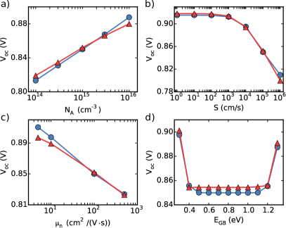
The results given by Eq. (35) provide insight into the precise role of grain boundaries in determining . For example, in all cases we consider, decreases logarithmically with the grain size . For the hotspot case, is independent of grain boundary defect energy level, seen in the saturation of for in Fig. 9(d), and is independent of the grain boundary length in the -direction. On the contrary, increases linearly with the grain boundary defect energy level in the regimes and , which implies that higher and lower defect energy levels increase the open-circuit voltage. Interestingly, in the hotspot regime, is increased with decreasing electron mobility (Fig. 9(c)). This is because a stronger electrostatic potential drop along the grain boundary is required to drive the current for lower electron mobility, and this leads to more suppression of hole density and recombination.
In Fig. 9(b), we reduce to values which correspond to capture cross sections which are unphysical (given the assumption of high ). However, we present these results for the purposes of validating the mathematical analysis of the model. We note that for small enough , bulk recombination dominates. More precisely, the junction depletion region and the neutral grain interior determine . Indeed, for the grain boundary energy level presented here, the grain boundary is in the hotpot regime for and the recombination of the grain interior depletion region is negligible (see insets of Fig. 8).
While Eq. (35) offers insight into how the different parameters controlling a grain boundary affect , an experimental verification is not straightforward. Indeed Eq. (35) does not encompass the diversity of grain boundaries contained in actual devices (grain boundary types, orientations, defect energy levels). Further work is necessary to examine more complex configurations than the one considered here. It should also be noted that our assumption of flat hole quasi-Fermi level depends on temperature (see Eq. (14)), so that our results are only applicable at sufficiently high temperatures. Generalizing the present analysis for grain boundaries with multiple defect levels and arbitrary orientations is the subject of ongoing work.
VI Conclusion
This work investigates the influence of grain boundaries on the efficiency of polycrystalline thin films solar cells. To this end we derived analytic expressions for the grain boundary dark recombination current and provided physical pictures for the charge carrier transport, both supported by numerical simulations. Within reasonable approximations we found that our analytic results give the proper functional dependence of the grain boundary recombination current on the parameters , and . We showed that for realistic surface recombination velocities, the grain boundary recombination dominates over the bulk recombination, and reduces the open-circuit voltage. We believe the physical pictures of charged grain boundaries, and the corresponding analytic results given here are not limited to CdTe and . Other materials such as polycrystalline Si, and GaAs bicrystals Grovenor (1985) exhibit grain boundary built-in potentials of several hundred . Our analysis could be extended to these materials as well. Further theoretical work with more complex grain boundary configurations is needed for experimental validation to be possible.
Acknowledgements.
B. G. acknowledges support under the Cooperative Research Agreement between the University of Maryland and the National Institute of Standards and Technology Center for Nanoscale Science and Technology, Award 70NANB10H193, through the University of Maryland.Appendix A Condition for Fermi level pinning at grain boundary defect energy level
We derive the critical defect density Eq. (5) that sets the pinning of the Fermi level to the grain boundary defect energy level. We consider the grain boundary at thermal equilibrium in the neutral region of the junction. The grain boundary electron and hole densities are related to their grain interior counterparts by the grain boundary built-in potential ,
| (36) | |||
| (37) |
where is the acceptor density, and . We assume the grain boundary core to be -type so that and are negligible. We define the difference between and , , which we will assume small compared to : , to rewrite Eq. (1) as
| (38) |
Using a depletion approximation and , the charge in the depleted regions surrounding the grain boundary is
| (39) |
We set the criterion to have close to the defect state, which yields the critical grain boundary defect density of states
| (40) |
We restrict the scope of this paper to defect densities larger than .
Appendix B Condition for nearly flat hole quasi-Fermi level
We specify the domain of validity of the assumption of flat hole quasi-Fermi level. In particular, we will consider when variations of across the grain boundary are smaller than . An expansion of across the grain boundary yields
| (41) |
where the gradient of at the grain boundary depends on whether we consider the linear regimes ( or ) or the hotspot regime.
For the regime , the gradient of is obtained by integrating the continuity equation for holes across the grain boundary over an infinitely small distance,
| (42) |
Assuming that the variation of across the grain boundary follows that of the electrostatic potential, the distance across the grain boundary where is given by a depletion approximation . The assumption of flat is therefore valid for
| (43) |
Replacing by in Eq. (43) gives the criterion for the regime .
In the hotspot regime, the same approach is used but the continuity equation is considered at the hotspot across the entire -direction. Because of the hotspot, the hole and electron currents integrated along the -direction are equal to half the recombination current. The gradient of across the grain boundary is therefore reduced by a factor
| (44) |
which leads to the criterion
| (45) |
for the assumption of flat hole quasi-Fermi level to be valid.
Appendix C Derivations for
Using the energy scale and definitions of Fig. 1(b), the carrier densities at the grain boundary are given by
| (46) | ||||
| (47) |
where is the electrostatic potential at the grain boundary. The reference of electrostatic potential is at the -contact away from the grain boundary. We now proceed to determine and .
Because of the pinning of the hole quasi-Fermi level to , the hole density is constant along the grain boundary () as shown in Fig. 4(b), and sets the electrostatic potential
| (48) |
shown in Fig. 10(a).
Within the depletion region and close to the -contact, electrons diffuse toward the grain boundary where they recombine, generating a hole current there. This occurs on a length corresponding to the point where electron and hole densities in the grain interior are equal. Using a depletion approximation in the depletion region of the junction in the grain interior, we find that at
| (49) |
where is the junction built-in potential (the dependence of on applied voltage is weak and can be neglected). Beyond this point we use the continuity equation for electrons to obtain ,
| (50) |
where the electron current component along the grain boundary is given by
| (51) |
In the above equation we assumed that the electron density across the grain boundary decays as , where
| (52) |
is the characteristic length associated with the electric field transverse to the grain boundary in the bulk region. This exponential decay assumes that is flat around the grain boundary, which coincides with the fact that the currents going to the grain boundary are small. The recombination term in Eq. (50) comprises the grain boundary recombination (first term) and the bulk recombination (second term). We used the fact that electrons are minority carriers at and around the grain boundary to obtain these simplified expressions. Integrating Eq. (50) in the -direction around the grain boundary leads to
| (53) |
where we neglected the currents in the -direction at the end of the grain boundary depletion region, and the bulk recombination. We introduce the effective diffusion length , where is the electron diffusion constant, and rewrite Eq. (53) as
| (54) |
Considering that at , and neglecting the diverging part of the solution of Eq. (54), we obtain
| (55) |
We verify the accuracy of Eq. (55) in Fig. 10(b) (blue dotted curve).
Inserting Eqs. (48) and (55) into Eq. (46) yields the electron density given in the main text
| (56) |
Because , the recombination at the grain boundary reads
| (57) |
which we integrate over the length of the grain boundary to obtain the recombination current
| (58) |
Equation (58) is the general result in the case .
Appendix D Derivations for
Here we provide the derivations of the analytical results presented in Sec. III.3. We start with the most general expression of the product , where and are given by Eqs. (46) and (47) respectively:
| (59) |
Assuming , the electron density at the grain boundary reads
| (60) |
From here on the derivation of follows the exact same steps as Appendix C starting with the continuity equation:
| (61) |
where . is the characteristic length associated with the electric field transverse to the grain boundary. Because the grain boundary built-in potential is not uniform in this regime, the transverse electric field depends on the location along the grain boundary. While does not correspond to a precise field, we find that it accurately determines the slopes of the electron quasi-Fermi level and the electrostatic potential along the grain boundary. The electron current is still given by Eq. (51) with the change of for . Integrating Eq. (61) around the grain boundary leads to
| (62) |
where we neglected the currents in the -direction at the end of the grain boundary depletion region, and the bulk recombination. We introduce the effective diffusion length , and assume that ††footnotemark: to rewrite Eq. (62) as
| (63) |
Considering that at we obtain
| (64) |
Since , we can equate Eqs. (46) and (47) to get
| (65) |
which yields the electrostatic potential along the grain boundary
| (66) |
Comparisons of Eq. (64) and Eq. (66) with numerical data are shown in Figs. 10(a) and 10(b) respectively (green solid curves). We see that the numerically computed potential and electron quasi-Fermi level are not linear over the entire length of the grain boundary, however the analytical results give a good approximation of the slopes near the depletion region.
Appendix E Bulk diffusive current Eq. (33)
Here we compute the integral Eq. (33) without assuming . We obtained the following results
| (68) |
for ,
| (69) |
for , and
| (70) |
for with
| (71) |
References
- Dharmadasa (2014) I. Dharmadasa, Coatings 4, 282 (2014).
- Kumar and Rao (2014) S. G. Kumar and K. K. Rao, Energy Environ. Sci. 7, 45 (2014).
- Geisthardt, Topič, and Sites (2015) R. M. Geisthardt, M. Topič, and J. R. Sites, IEEE J. Photovolt. 5, 1217 (2015).
- Topič, Geisthardt, and Sites (2015) M. Topič, R. M. Geisthardt, and J. R. Sites, IEEE J. Photovolt. 5, 360 (2015).
- Yoon et al. (2013) H. P. Yoon, P. M. Haney, D. Ruzmetov, H. Xu, M. S. Leite, B. H. Hamadani, A. A. Talin, and N. B. Zhitenev, Sol. Energ. Mat. Sol. Cells 117, 499 (2013).
- Zywitzki et al. (2013) O. Zywitzki, T. Modes, H. Morgner, C. Metzner, B. Siepchen, B. Späth, C. Drost, V. Krishnakumar, and S. Frauenstein, J. Appl. Phys. 114, 163518 (2013).
- Li et al. (2014) C. Li, Y. Wu, J. Poplawsky, T. J. Pennycook, N. Paudel, W. Yin, S. J. Haigh, M. P. Oxley, A. R. Lupini, M. Al-Jassim, S. J. Pennycook, and Y. Yan, Phys. Rev. Lett. 112, 156103 (2014).
- Visoly-Fisher, Cohen, and Cahen (2003) I. Visoly-Fisher, S. R. Cohen, and D. Cahen, Appl. Phys. Lett. 82, 556 (2003).
- Moutinho et al. (2010) H. Moutinho, R. Dhere, C.-S. Jiang, Y. Yan, D. Albin, and M. Al-Jassim, J. Appl. Phys. 108, 074503 (2010).
- Jiang et al. (2004a) C.-S. Jiang, R. Noufi, J. AbuShama, K. Ramanathan, H. Moutinho, J. Pankow, and M. Al-Jassim, Appl. Phys. Lett. 84, 3477 (2004a).
- Tuteja et al. (2016) M. Tuteja, P. Koirala, V. Palekis, S. MacLaren, C. S. Ferekides, R. W. Collins, and A. A. Rockett, J. Phys. Chem. C 120, 7020 (2016).
- Sadewasser et al. (2011) S. Sadewasser, D. Abou-Ras, D. Azulay, R. Baier, I. Balberg, D. Cahen, S. Cohen, K. Gartsman, K. Ganesan, J. Kavalakkatt, W. Li, O. Millo, T. Rissom, Y. Rosenwaks, H.-W. Schock, A. Schwarzman, and T. Unold, Thin Solid Films 519, 7341 (2011).
- Leite et al. (2014) M. S. Leite, M. Abashin, H. J. Lezec, A. Gianfrancesco, A. A. Talin, and N. B. Zhitenev, ACS Nano 8, 11883 (2014).
- Galloway, Edwards, and Durose (1999) S. Galloway, P. R. Edwards, and K. Durose, Sol. Energ. Mat. Sol. Cells 57, 61 (1999).
- Haney et al. (2016) P. M. Haney, H. P. Yoon, B. Gaury, and N. B. Zhitenev, J. Appl. Phys. 120, 095702 (2016).
- Gloeckler, Sites, and Metzger (2005) M. Gloeckler, J. R. Sites, and W. K. Metzger, J. Appl. Phys. 98, 113704 (2005).
- Taretto and Rau (2008) K. Taretto and U. Rau, J. Appl. Phys. 103, 094523 (2008).
- Rau, Taretto, and Siebentritt (2009) U. Rau, K. Taretto, and S. Siebentritt, Appl. Phys. A 96, 221 (2009).
- Troni et al. (2013) F. Troni, R. Menozzi, E. Colegrove, and C. Buurma, J. Electron. Mater. 42, 3175 (2013).
- Fossum and Lindholm (1980) J. G. Fossum and F. A. Lindholm, IEEE Trans. Electron Devices 27, 692 (1980).
- Green (1996) M. A. Green, J. Appl. Phys. 80, 1515 (1996).
- Edmiston et al. (1996) S. Edmiston, G. Heiser, A. Sproul, and M. Green, J. Appl. Phys. 80, 6783 (1996).
- Thorpe, Fahrenbruch, and Bube (1986) T. P. Thorpe, A. L. Fahrenbruch, and R. H. Bube, J. of Appl. Phys. 60, 3622 (1986).
- Jiang et al. (2004b) C.-S. Jiang, R. Noufi, K. Ramanathan, J. A. AbuShama, H. R. Moutinho, and M. M. Al-Jassim, Applied Physics Letters 85, 2625 (2004b).
- Jiang et al. (2013) C. S. Jiang, H. R. Moutinho, R. G. Dhere, and M. M. Al-Jassim, IEEE J. Photovolt. 3, 1383 (2013).
- Yang (1978) E. S. Yang, Fundamentals of semiconductor devices (McGraw-Hill Companies, 1978).
- Moseley et al. (2015) J. Moseley, W. K. Metzger, H. R. Moutinho, N. Paudel, H. L. Guthrey, Y. Yan, R. K. Ahrenkiel, and M. M. Al-Jassim, J. Appl. Phys. 118, 025702 (2015).
- Note (1) Because holes are majority carriers in the bulk of the absorber, the hole quasi-Fermi level is flat equal to there. We derived in Appendix B a criterion under which the hole quasi-Fermi level is flat across the grain boundary, so that the bulk quasi-Fermi level extends to the grain boundary core.
- Neugroschel and Mazer (1982) A. Neugroschel and J. Mazer, IEEE Trans. Electron Devices 29, 225 (1982).
- Metzger and Gloeckler (2005) W. Metzger and M. Gloeckler, J. Appl. Phys. 98, 063701 (2005).
- Fonash (1981) S. J. Fonash, Solar cell device physics (Academic Press, 1981).
- Tarr and Pulfrey (1980) N. G. Tarr and D. L. Pulfrey, IEEE Trans. on Electron Devices 27, 771 (1980).
- Grovenor (1985) C. R. M. Grovenor, J. Phys. C: Solid St. Phys. 18, 4079 (1985).