A Scanning Quantum Cryogenic Atom Microscope
Abstract
Microscopic imaging of local magnetic fields provides a window into the organizing principles of complex and technologically relevant condensed matter materials. However, a wide variety of intriguing strongly correlated and topologically nontrivial materials exhibit poorly understood phenomena outside the detection capability of state-of-the-art high-sensitivity, high-resolution scanning probe magnetometers. We introduce a quantum-noise-limited scanning probe magnetometer that can operate from room–to–cryogenic temperatures with unprecedented DC-field sensitivity and micron-scale resolution. The Scanning Quantum Cryogenic Atom Microscope (SQCRAMscope) employs a magnetically levitated atomic Bose-Einstein condensate (BEC), thereby providing immunity to conductive and blackbody radiative heating. The SQCRAMscope has a field sensitivity of 1.4 nT per resolution-limited point (2 m), or 6 nT/ per point at its duty cycle. Compared to point-by-point sensors, the long length of the BEC provides a naturally parallel measurement, allowing one to measure nearly one-hundred points with an effective field sensitivity of 600 pT for each point during the same time as a point-by-point scanner would measure these points sequentially. Moreover, it has a noise floor of 300 pT and provides nearly two orders of magnitude improvement in magnetic flux sensitivity (down to ) over previous atomic probe magnetometers capable of scanning near samples. These capabilities are, for the first time, carefully benchmarked by imaging magnetic fields arising from microfabricated wire patterns, in a system where samples may be scanned, cryogenically cooled, and easily exchanged. We anticipate the SQCRAMscope will provide charge transport images at temperatures from room–to–4 K in unconventional superconductors and topologically nontrivial materials.
I Introduction
Quantum sensors comprised of nitrogen-vacancy (NV) color centers in diamond have joined scanning Superconducting Quantum Interference Devices (SQUIDs) in advancing high-sensitivity magnetometry into the nanoscale regime Grinolds et al. (2013); Vasyukov et al. (2013); Kirtley et al. (2016). BECs have also been used for magnetometry Estève et al. (2004); Günther et al. (2005); Wildermuth et al. (2005, 2006); Aigner et al. (2008). We add to this quantum metrology toolbox a carefully calibrated cryogenic scanning magnetometer that exploits the extreme sensitivity of these quantum gases to external fields. The SQCRAMscope operating principle is sketched in Fig. 1. Inhomogeneous magnetic fields from a nearby source exert a Zeeman force on atoms Bose-condensed in a smoothly varying harmonic trap. The atoms move in response, distorting the otherwise smooth wavefunction of the BEC. The BEC density is then imaged by recording the absorption of resonant light using a CCD camera. The local density may be related to field through the BEC equation of state. A 2D-field map is created by raster-scanning the relative position of the BEC and the source with a duty cycle limited by the time needed to recreate the BEC after the destructive absorption imaging process. Assuming no -dependence of the source, application of the Biot-Savart law, conservation of current, and a measurement of the distance between BEC and sample allows one to convert an - map of the field component into a 2D map of the current flow (or magnetic domains) in the source Estève et al. (2004); Günther et al. (2005); Wildermuth et al. (2005, 2006); Aigner et al. (2008).
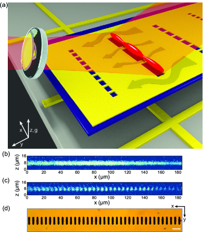
The BEC is confined in a high-aspect-ratio, cigar-shaped trap formed using an atom chip-based magnetic microtrap Fortágh and Zimmermann (2007); Naides et al. (2013) (see Appendix A). This quasi-1D Bose gas lies within the quasicondensate regime because the transverse trap frequency is 157 larger than the longitudinal trap frequency , the chemical potential is similar in magnitude to , and the gas temperature is 2.6 lower than . As such, density fluctuations are suppressed below the quantum shot-noise limit Gerbier (2004); Bloch et al. (2008); Jacqmin et al. (2011), enhancing field sensitivity (see Appendix C). The equation of state in the quasicondensate regime we employ is given by , where is the 3D -wave scattering length, is the line density, and is the total potential 111We actually employ the full expression given in Ref. Gerbier (2004); see also Ref. Krüger et al. (2010).. This potential is the sum of the well-characterized trapping potential and the magnetic potential to be measured. For the employed atomic state and at the small fields that are measured, the magnetic potential is linearly proportional to field, i.e., . Small inhomogeneous fields primarily perturb the trap potential only along the weakly trapped axis because . Thus, the atomic position can only move a minuscule amount in response to weak transverse fields. Imaging perturbations to the BEC density along therefore provides a measurement of a vector component of the magnetic potential along . The spatial density modulation is measured by absorption imaging with a resonant laser at an intensity well above saturation and reflected at shallow angle from the reflective sample surface. Much care is taken to account for the presence of the standing wave intensity pattern of the reflecting beam. See Appendix B.
The responsivity of the magnetometer is given by . In the limit of low atom number, the equation of state can be approximated by , and the responsivity becomes , where is the effective 1D-interaction strength . We employ two different traps in this work, one whose trap frequencies are optimized for high sensitivity, and the other for extended dynamic range.
In the following, we benchmark a number of the SQCRAMscope’s attributes. These include: 1) The responsivity [nT/(atom/m)] of the atomic density to magnetic field variations. 2) The field sensitivity (minimum detectable field). This is quoted in several forms depending on operation modality: field sensitivity [nT] in a single-shot per resolution-limited point size (RLP), field sensitivity [nT/Hz1/2] per RLP, and field sensitivity [nT/Hz1/2] over a finite scan area (to be explained below). 3) Magnetic flux sensitivity [/Hz1/2] both per RLP and over a finite scan area, where is the magnetic flux quantum. 4) The magnetic field noise floor [pT] via Allan deviation measurements, which determines the minimum detectable field provided by averaging. 5) Spatial resolutions [m] of both the field at the BEC and the current in the sample a distance away. These resolutions are given according to the Rayleigh criterion, which determines the RLP. 6) Current density resolution [nA/m], which is the current density resolvable by measuring the field a distance from the surface. 7) The accuracy [%], which measures the ability to determine a known field within a certain percentage error. 8) The repeatability [nT] quantifies the ability to measure the same field in successive runs and is defined as the average standard deviation in the data. 9) The dynamic range [nT] is the range in field in which the sensor has a linear response .
To determine these specifications, several other quantities required careful calibrations, including the absorption imaging magnification, the BEC–to–surface distance , the per-pixel photon shot noise at our CCD camera, the atomic density noise per pixel, and contributions from patch fields. Information regarding these are reported in the appendices, along with details of the BEC production, the calibration sample, imaging theory, and cryogenic scan results.
The SQCRAMscope will enable the high-sensitivity study of strongly correlated and topologically nontrivial materials in unexplored regimes of high temperature and low frequency. For example, domain structure and transport near twin boundary interfaces in underdoped Fe-arsinide superconductors can be explored as the –150 K nematic transition is crossed Chu et al. (2010). Other unconventional superconductors and complex oxide interfaces (e.g., LAO/STO) Bert et al. (2011) may be explored at high temperatures, as well as the metal-to-insulator transition in VO2 Qazilbash et al. (2007). Both transport and static magnetization at the 100-K ferromagnetic-metallic and antiferromagnetic-insulating transition in colossal magnetoresistive systems may be imaged. Investigations of topologically protected transport should be possible Dellabetta et al. (2012); Nowack et al. (2013), as should investigation of the electronic hydrodynamic flow in graphene above LN2 temperatures Zaanen (2016). Lastly, the SQCRAMscope will also find use in engineering hybrid quantum systems, in coupling BECs to photonic topological metamaterials, and in studying the Casimir-Polder force Lin et al. (2004); Obrecht et al. (2007a).
II Experimental Results
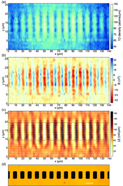
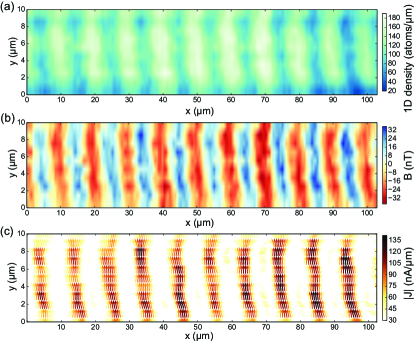
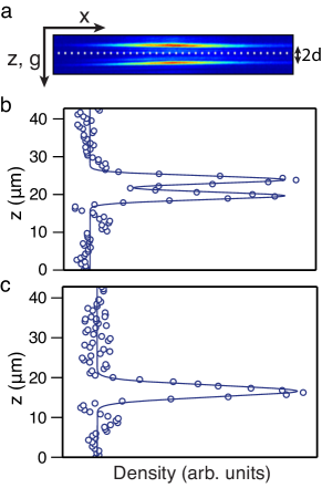
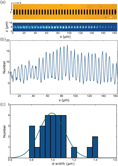
Figure 2 shows a typical magnetic field scan above a room-temperature microwire array, and the resulting image of the current density flowing through the wires. The FWHM point-spread resolution of the atomic density and magnetic field is 2.2(1) m, and can be improved in the future by more than a factor of two using a custom-tailored lens system. The current density map has a lower spatial resolution than the field maps, stemming from the convolution of the field resolution with the typical distance m between the atoms and sample. Distances as short as 0.8(1) m, shown in Fig. 1(c), may be used, providing a source resolution of 2.3(1) m. Current flow through the microwires is clearly visible in Fig. 2(c), as is the fanning out of current into the bulk. Patches of lower current density may result from higher-resistance grains in the polycrystalline film, as measured in Ref. Aigner et al. (2008). (See Appendices A and B for resolution measurements, distance calibration, and scan done with sample at cryogenic temperature.)
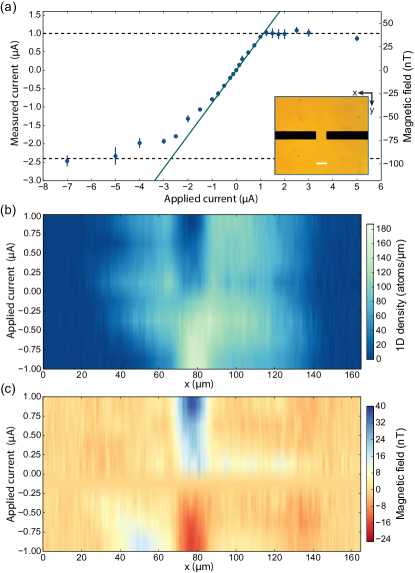
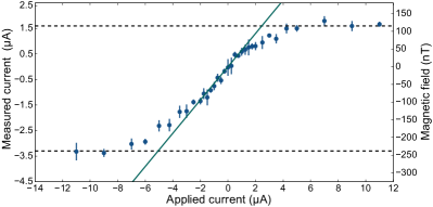
The accuracy, repeatability, linearity, and dynamic range of the magnetometer are shown in Fig. 3. The green line is a fit to the linear region of the measured versus applied current data and has a slope of 0.88(2). This implies an accuracy of 11(2)% and a responsivity only 11(2)% lower than that predicted for the high-sensitivity trap, nT/(atom/m). The fields and current densities reported in Fig. 3 correspond to those calculated with a finite-element solver for the employed gold microwire dimensions to within 10%.
The linear part of the dynamic range is between approximately A ( nT). The upper limit arises due to lack of atoms in the high-field regions, while the lower limit arises due to all the atoms pooling into the low-field regions, as may be seen in panel b. The extended-dynamic-range trap provided a 3-larger linear dynamic range, though with a responsivity 3 worse (see Appendix C). We have employed a thermal gas to increase the dynamic range by 50, though at worse resolution and with 100-fold-worse responsivity, as also noted in Refs. Wildermuth et al. (2006); Aigner et al. (2008).
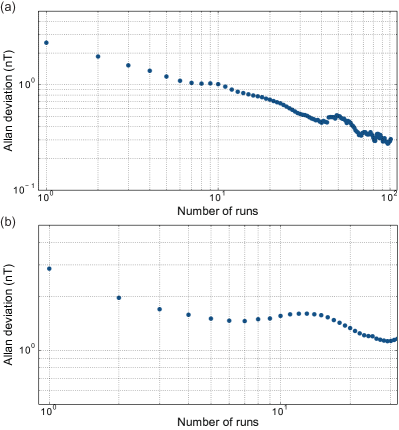
The repeatability, or average standard deviation in the data about the linear fit, is 2.3(3) nT per pixel, and the stability of the field measurement, measured as Allan deviation, is 1.1(1) nT after 30 experimental runs. To calculate repeatability and Allan deviation, we extract the (shot-to-shot) deviations of the measured total current in the 12 m wire by averaging the difference between the measured field profile and the predicted field profile (of the 12 m wire); repeatability and Allan deviation are spatial averages over the width of the calibration wire.
With no current applied to sample, we measure a single-shot minimum sensitivity of 2.8(5) nT per pixel. (No spatial averaging is performed for this measurement.) This value is consistent with two independently measured quantum-noise-limited sources: photon shot noise accounts for 2.5(4) nT per pixel, while atom density noise is 1.7(7) nT per pixel. Due to the quasicondensate nature of the gas, this noise is a factor of 2 below that expected for shot noise in the higher density regions of the BEC; hence the use of “Quantum” in the name of the scanning microscope. (See Appendix C for Allan deviation and noise measurements.)
The noise floor is measured also by Allan deviation, and the result is 300 pT per pixel after 100 runs. (No spatial averaging is performed for this measurement.) This noise floor translates into a 2-nA minimum detectable current from an infinitely thin wire or 80 horizontally oriented 1- dipoles, when the BEC is located m from these sources.
Since the particular pixel sizes are not intrinsic to the sensor itself, we now convert these ‘per pixel’ values to field sensitivities per our resolution-limited point (RLP) size of 2.2 m. The RLP is set by our spatial resolution for field measurements. There are 4.1(2) pixels per RLP for our lens system, and so the single-shot field sensitivity per RLP is a factor of lower, or 1.4(1) nT. This is equivalent to 6.1(1) nT/Hz1/2 per RLP when considering the s duty cycle.
The magnetometer simultaneously provides independent RLPs of information because the quasi-1D BEC may be several hundred microns in length while the imaging resolution is on the micron scale. This provides an advantage over point-by-point scanning magnetometers such as SQUIDs because the SQCRAMscope can repeatedly measure these points during the time it takes the scanning SQUID to sequentially measure the points once. is the integration time per point. That is, if , then the SQCRAMscope has enough time to average the signal of each RLP times during the same time it would take the SQUID to record a single scan of the points. This lowers the field sensitivity by a factor of . In terms of sensitivity per root Hz, the enhancement factor is . This results in a field sensitivity of 590(80) pT/ per RLP for a line scan, given our and . Thus, high-sensitivity, high-resolution, and wide-area scans of condensed-matter samples can be made within a few hours. Future improvements can expedite this by reducing the duty cycle and elongating the usable BEC length. In Fig. 4, we include this parallel measurement-based sensitivity in addition to the single-shot sensitivity to properly account for the parallel-scanning advantage of our sensor: that is, what one cares about for comparing a parallel scanning probe microscope is the sensitivity per point in the same time it would take a comparable point-by-point sensor to scan the same number of points.
III Comparison to other techniques
We now highlight other demonstrated features of the SQCRAMscope. Because the samples are physically detached from the chip, we can rapidly replace the sample without disturbing the BEC production apparatus in five days. This is much faster than the up to several months of current systems whose samples are attached directly to the atom chip. Secondly, the sample temperature may be independently controlled and stabilized, in contrast to samples attached to an atom chip, where trapping wire currents can uncontrollably heat the sample. In the case of superconducting atom chip experiments such as in Refs. Nirrengarten et al. (2006); Mukai et al. (2007); Roux et al. (2008); Müller et al. (2010); Reichel and Vuletic (2010); Cano et al. (2008); Jessen et al. (2013); Minniberger et al. (2014); Chan et al. (2014), the sample temperature would be fixed to that of the superconducting chip and not tunable. The SQCRAMscope allows any 1-cm2 area, 150-m-thin sample made of UHV-compatible material to be imaged from room–to–cryogenic temperatures. We have demonstrated here the functionality of the SQCRAMscope at room temperature and 35 K (see Appendix A) and believe operation down to 4 K will soon be possible with the addition of a heat shield Naides et al. (2013). Lastly, we mention that because what the SQCRAMscope measures are nT-strength, short-wavelength deviations in the mean field along the trap axis, the microscope is insensitive to much larger—up to hundreds of Gauss—background or long-wavelength fluctuating fields along this axis. This feature obviates the need for careful magnetic field shielding of the apparatus.
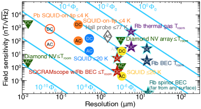
In the following, we compare the scanning magnetometry capability of the SQCRAMscope to other high-source-resolution, high-sensitivity scanning probe magnetometers relying on field sensing of arbitrary sources rather than magnetic resonance of spins. (For the latter, see Refs. Rugar et al. (2004); Lovchinsky et al. (2016) for nanoscale diamond NV and magnetic force microscope-based techniques). See Fig. 4. Imaging the Larmor precession of spinor BECs has been used to measure magnetic fields with high sensitivity Vengalattore et al. (2007), though the technique has yet to be demonstrated near any surface and so the technique’s sensitivity limit near a sample is unclear.
By contrast, spin-polarized BECs have been used to image the field from and current flow through nearby room-temperature gold wires using the technique discussed here Günther et al. (2005); Wildermuth et al. (2005, 2006); Aigner et al. (2008); Ockeloen et al. (2013). These works employed a BEC (thermal gas) (3.5) m from the room-temperature wires, resulting in a field sensitivity of 4 (42) nT/ per RLP at a current density resolution of 11 (5) m to simultaneously measure 67 (200) RLPs. We note that Refs. Wildermuth et al. (2005, 2006); Aigner et al. (2008) do not include extensive calibration data and so best-case estimates are used for comparison; i.e., we assume the reported resolution is FWHM rather than, e.g., 1-, and that the reported calculated sensitivities are realized in their experiments (our calculated values are better than what we measure). As for our parallel sensor, the field sensitivity is obtained by multiplying their calculated minimum field by the square root of the ratio of duty cycle to number of simultaneously measured RLPs (obtained from Refs. Wildermuth (2005); Aigner (2007)). Again, the latter are defined as the usable length of the cloud divided by the spatial resolution, and is included because this instrument is intended as a scanning probe and what matters is the entire time it takes to scan an area, not a point. To facilitate comparisons to SQUIDs below, we estimate their magnetic flux sensitivity to be by multiplying the minimum field sensitivity by the square of the current density resolution.
By comparison, our present work has lowered the minimum achieved field sensitivity to 0.6(1) nT per RLP for simultaneously measuring 91 points at a superior resolution of 2.3(1) m (Rayleigh criterion). Moreover, we rigorously calibrated this from the use of a known test source in the form of gold microwires at both room and cryogenic temperatures. This results in nearly a 100-fold magnetic flux sensitivity improvement to . Lastly, unlike these previous experiments, our result derives from a true sample, one not part of the atom chip itself and so may be scanned for wide-area imaging, cryogenically cooled (to a temperature different than the chip temperature), and easily exchanged. All these features make our SQCRAMscope a uniquely versatile scanning probe atom microscope for condensed matter materials.
The point-by-point scanning technique of SQUID magnetometers Kirtley et al. (2012); Vasyukov et al. (2013); Kirtley et al. (2016) provides high-AC-sensitivity (10–100 worse at DC) imaging at length scales from a few-microns Kirtley et al. (2012) to 100-nm Vasyukov et al. (2013); Kirtley et al. (2016) and down to dilution refrigerator temperatures. (New SQUIDs-on-a-tip have achieved AC flux sensitivities of below (DC, ) Vasyukov et al. (2013), though with the use of fragile Pb-based superconductors.) The superior low-temperature and high-frequency imaging abilities of these scanning SQUIDs is complemented by the higher DC sensitivity and high-temperature compatibility of the SQCRAMscope. Specifically, these high-resolution SQUIDs lose sensitivity above sample temperatures of 20 K due to weak thermal links to the sample, bringing the SQUID close to its superconducting critical temperature Iranmanesh et al. (2014). (High-Tc SQUIDs provide less sensitivity.) Moreover, SQUID sensitivity decreases by roughly two orders of magnitude at DC due to 1/ noise below 100 Hz. We also note that while SQUIDs must often employ large fields to function, the SQCRAMscope is minimally invasive, because the field at the trap bottom—and at the nearby sample—can be as small as 1 G. Conversely, however, our current SQCRAMscope is incompatible with the application of large fields perpendicular to the sample, though fields up to nearly a kG can be applied along the trap axis, in the plane of the sample.
Nanoscale scanning NV diamond magnetometers are also compatible with samples from room–to–cryogenic temperatures Pelliccione et al. (2016), but are additionally operable outside ultrahigh vacuum. They provide a field sensitivity of a few nT/ with resolution down to a few nm near surfaces at frequencies above 10 kHz Grinolds et al. (2013); Shields et al. (2015); Lovchinsky et al. (2016) and 2-T at DC, with more than ten-fold improvements predicted Taylor et al. (2008). Arrays of NV sensors have been used for parallel, wide-area imaging of AC fields Pham et al. (2011). In Fig. 4, the three green-triangle markers denote the sensitivity and resolution for these NV arrays for single-point measurements (light-blue outline), at higher effective AC sensitivity (15 nT/ per RLP) with respect to the time it would take to integrate the same area as the raster line-scanned SQCRAMcope (shown with blue outline), and at still higher effective AC sensitivity (1 nT/ per RLP) with respect to point-by-point sensors (no outline). The SQCRAMscope complements this probe with its nearly 1000-fold higher DC-sensitivity to fields that cannot be rapidly modulated. While the present 2-micron-scale SQCRAMscope resolution is far worse than single-NV probes, a SQCRAMscope with sub-micron resolution is possible as well as with AC sensitivity at bandwidths up to 10 kHz via dispersive imaging Vengalattore et al. (2007) and up to MHz using Rabi spectroscopy Treutlein et al. (2004).
IV Outlook
The unprecedentedly low DC-field sensitivity and wide temperature compatibility of the SQCRAMscope will provide the ability to investigate phenomena in materials outside the reach of the current capabilities of, e.g., scanning SQUIDs. We highlight here one such application for which the SQCRAMscope is uniquely suited. The possible emergence of the unconventional pair-density-wave superfluid state in cuprate, high-T superconductors and the theory of striped superconductors is the subject of much interest and speculation Berg et al. (2007, 2009). A key signature of such a state would be the spontaneous generation of DC currents around domains of the emerging chiral superconductor as the temperature is tuned below 30 K. Imaging transport may reveal these spontaneously generated current loops. However, while the length scale of current loops may be on the few micron scale and thus within our detection range, it is not theoretically known what might be the magnitude of the currents and detection has been elusive Kivelson (2016). Thus, one requires a sensor of highest DC sensitivity to maximize one’s chances of observation and to bound this magnitude if no signal is observed. The SQCRAMscope is uniquely positioned to tackle this important measurement: its DC sensitivity is two–to–three orders of magnitude greater than SQUIDs and NV diamonds, and scanning a wide field-of-view will be necessary to hunt for the chiral currents as they emerge, a task appropriate for the SQCRAMscope with its parallel sensing capability. Moreover, the high AC sensitivity of those sensors is not relevant since the spontaneously generated currents cannot be modulated, and SQUIDs become less sensitive at the elevated temperature at which the transition is predicted to occur. In summary, the SQCRAMscope will enable the study of strongly correlated and topologically nontrivial materials in regimes of parameter space unamenable to any other current technique.
Acknowledgements.
We thank M. Naides, J. DiSciacca, S. Qiao, and J. Straquadine for experimental assistance, and P. Abbamonte, J. Analytis, S. L. Cooper, I. Fisher, J. Kirtley, S. Kivelson, M. Lukin, K. Moler, R. Walsworth, and A. Yacoby for stimulating discussions. This work was supported by the U.S. Department of Energy (DOE), Office of Science, Basic Energy Sciences (BES), under Award #DE-SC0012338 (equipment and materials, and support for B.L.L.). R.W.T., A.J.K. and B.L.L. acknowledge support from the Gordon and Betty Moore Foundation through Grant GBMF3502.Appendix A Experimental Methods
A.1 Cryogenic scan
The cryogenic capability of the trapping apparatus was demonstrated in Ref. Naides et al. (2013). While the majority of the data shown here were taken at room temperature, we performed a magnetometry scan, shown in Fig. 5, at 35 K with no discernible loss in capability, other than the observation of a horizontal drift in the relative BEC–sample position. This is likely due to the slow settling of thermally contracting parts of the apparatus, and can be mitigated by waiting longer before imaging. Temperature is measured with in-vacuum thermometers contacted to the cold head and calibrated to the temperature at the sample tip Naides et al. (2013).
A.2 Calibration sample
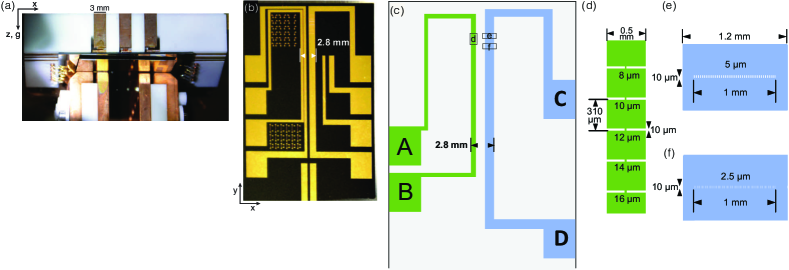
The sample substrate is a 150-m thick wafer of oxidized intrinsic silicon. The gold calibration wires are fabricated directly onto the sample substrate using photolithography, as shown in Fig. 6(a), and positioned, using a three-axis translation stage, such that the calibration wires are 300 m below the atom chip. See Ref. Naides et al. (2013) for more details. We have verified that the quasi-1D BEC, located below the calibration wires, is not fragmented by meandering currents in the atom chip’s microwires at this far distance. The stage can move the sample substrate 3.8 mm in and 5.4 mm in allowing any sample feature within this area to be placed in proximity to the BEC. (Future improvements will increase this area by 5.) Coarse positioning of the BEC with respect to the microwire arrays on the calibration sample is made by fluorescence imaging from below the sample. Fine positioning is performed by fitting magnetic field profiles obtained from magnetometry of current flowing through sample calibration features. Microwire centers are found to within 1 m.
Vertical vibrations of the cantilevered calibration sample at frequencies larger than 1 Hz are 150 nm RMS, much less than our imaging resolution, and may be ignored Naides et al. (2013). Thermal expansion of the atom chip and the sample mount assemblies cause small drifts of sample position relative to the BEC on a time scale much slower than the duty cycle. However, these are easily measured via imaging and cancelled via feedforward to the bias field that controls the atom chip trap height between each run. More difficult to cancel are vertical drifts at the time scale of the duty cycle. These cause 0.5-m shot-to-shot fluctuations of the BEC position relative to the sample. Fortunately, these may be accounted for in the data analysis on a shot-to-shot basis since is imagined at the same time as the atomic density. The BEC scan data and accuracy calibrations reveal that the horizontal movements of sample stage with respect to the imaging system is less than 0.5 m shot-to-shot at room temperature.
The data for Figs. 1–3 were taken using the sample shown in Fig. 6(b). We used e-beam evaporation, photolithography, and ion-milling to fabricate the 400-nm-thick gold calibration wire patterns. The calibration sample contains two 1.2-mm-wide strips of gold, as sketched in Fig. 6(c). Gaps in the gold of these strips define microwires and microwire arrays of different sizes and spacings, as shown in Fig. 6(d)–(f). Current flowing through the constricted regions provides the signal for all measurements. The microwire arrays in panels e and f are periodic with equal wire width and spacing. The magnification calibration in Fig. 7 and resolution calibration in Fig. 12(b)-(d) was taken with a different calibration sample (not shown), which contained an array of microwires of width 2.0(1) m and length 10 m spaced by 20.0(2) m from each other.
A.3 Quasi-1D BEC production
Atom chip trapping of ultracold gases of 87Rb atoms proceeds in a manner similar to that described in Ref. Naides et al. (2013). Briefly, atoms in the ground state at 30 K are loaded into an optical dipole trap (ODT). (The -factor is in this weak-field seeking state.) These atoms are then transported 33 cm by moving the lens focusing the ODT. The atoms pass through a gate valve into a science chamber. The gate valve allows samples within the science chamber to be exchanged without breaking the ultrahigh vacuum of the production chamber. The room-temperature vacuum of the science chamber is below Torr, sufficient for BEC production using the atom chip; see Refs. Fortágh and Zimmermann (2007); Reichel and Vuletic (2010) for details on BEC production using atom chips. This pressure decreases upon the cryogenic cooling of the sample Naides et al. (2013).
The ODT is located 3.5-mm below the atom chip so as not to heat the sample and chip with scattered light. To bring the atoms closer to the sample, the atoms are transferred from the ODT to a magnetostatic harmonic trap formed by an H-shaped Cu-wire and an homogeneous field. The wire is mounted just above the atom chip, which faces downwards. See Fig. 6(a) and Ref. Naides et al. (2013). This macrowire magnetic trap is moved upwards to within a few hundred microns of the chip. Atoms are then transferred to an atom-chip-based trap. The trap in the - plane is formed with three wires: a bias magnetic field along is created by macrowires on either side of a 150-m-wide wire whose current flows opposite to the macrowires; all current in these wires can be rapidly shut off to drop the atoms for short time-of-flight (TOF) imaging. Weak confinement along the axis of the quasi-1D BEC is provided by independently controlled orthogonal end-cap wires. RF evaporation produces BECs with up to a few atoms. The entire procedure is typically repeated every 20 s, though 16-s cycle times can be used.
We create BECs in two different traps. The first, the high-sensitivity trap, is optimized to minimize single-shot repeatability and detectable field. (Lower transverse trap frequency leads to higher sensitivity through the minimization of mean-field energy, but also reduces the dynamic range due to lower density.) The trap frequencies are Hz and Hz, and we create quasi-1D BECs of atoms at temperature 12(1) nK. (Larger BECs are possible, but the lower population ensures operation within the quasicondensate regime.) This temperature is far below the quasidegeneracy temperature 1.5(1) K—the critical temperature for phase fluctuations is 9.0(5) nK—and 2.8-below the temperature associated with , 33.7(6) nK Gerbier (2004); Bloch et al. (2008); Jacqmin et al. (2011). (See Appendix C for discussion of temperature measurement.) The chemical potential is 32(1) nK, similar to and sufficiently low for the quasicondensate equation of state to hold to high accuracy Gerbier (2004). Shot-to-shot temperature and number fluctuations do not affect the magnetometry because they are not sufficiently large to change the applicable equation of state for the gas and are recorded and accounted for on a shot-by-shot basis. The second trap, with frequencies Hz and Hz, is optimized to extend the dynamic range while also providing 1D-Bose gases within the quasicondensate regime.
After quasicondensate preparation, the current in the calibration wire is adiabatically ramped-up in 300 ms. The BEC is then raised to a distance 1.7(2)-m below the sample surface for the high-sensitivity trap and 1.3(4)-m below the sample for the extended dynamic range trap. Lifetime within the trap is greater than 700 ms at m; the attractive Casimir-Polder potential does not pose a severe lifetime limit at this distance Lin et al. (2004).
Appendix B Imaging Calibration
B.1 Imaging
BECs are held in the magnetic field of the calibration sample for 250 ms before the trap and sample fields are rapidly removed for BEC imaging. This is much longer than the density response time of 0.5 ms, the time atoms take to move 1 m at the speed of sound in the BEC Ketterle et al. (1999). We allow the atoms to fall for 150 s. The imaging beam is on for 20 s, during which the atoms diffuse by 500-nm RMS, much less than our imaging resolution (see below). During this brief TOF, the atoms fall 1 m due to gravity and an initial velocity imparted from magnetic gradients when the trapping fields are turned off. The imaging takes place when the atoms are 2.5 m from the sample (see below). Ballistic expansion during this time is approximately 200 nm and also small compared to the imaging resolution.
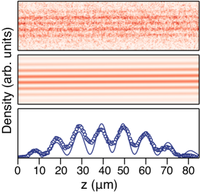
Accurate measurement of the imaging magnification via rate-of-fall-under-gravity is problematic due to the small field-of-view in the vertical direction. This is the result of our high magnification and the use of only a small fraction of our CCD array so that fast kinetics mode can be used for fringe suppression. We therefore measure the magnification by imprinting a density modulation of known periodicity onto the gas and imaging its density in situ with no TOF. See Fig. 7. The density modulation is created by using the magnetic fields from a microfabricated microwire array on a calibration sample. Error in the spatial frequency measurement, combined with uncertainty in the microwire dimensions, leads to a 0.8% uncertainty in magnification.
Imaging the BEC near a surface is complicated by the presence of diffraction fringes from the sample edge. Reflecting the absorption imaging beam at a small angle removes the fringes from the field of interest Smith et al. (2011), but it introduces a standing wave intensity pattern perpendicular to the chip. (Non-reflective samples may be coated with a thin insulator before mirroring with gold; a gold mirror and insulating layer need only be a few hundred nm, far thinner than our optical resolution.) This complicates the usually simple technique of absorption imaging commonly employed in free space, away from reflective surfaces. Moreover, due to the reflection, the polarization of the imaging beam must be linear and parallel to the sample surface to prevent polarization imperfections at the position of the atoms. To define the quantization axis during imaging, we maintain a small B-field along this polarization direction. The light drives -transitions, resulting in non-closed-cycle transitions. However, we have used numerical simulations of the optical Bloch equations to account for the optical pumping out of the trapped state during the imaging time; we use in our calculations the effective cross section obtained from these simulations. (This also accounts for the term in Ref. Reinaudi et al. (2007).) We now describe how to perform absorption imaging in the presence of the standing wave pattern. Fig. 8 depicts the imaging geometry.
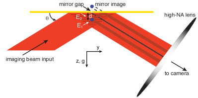
The main points that must be considered are: 1) The atoms appear in two images on the CCD, a mirror image from field , and a real image from the reflected field , as shown in Fig. 8. By mirror image we mean that the light scatters first from the atoms before reflecting off the mirror into the imaging system. We use the average of the mirror image and the real image for the data in this work. 2) The mirror is finite in extent and therefore acts as a Fourier filter for shallow-angle components that are not reflected into the imaging system Smith et al. (2011). That is, the upward scattering fields from and are not imaged onto the CCD since their negative components do not get reflected from the mirrored sample. While this can lead to image distortion, it is a negligible perturbation for mirrors as long and ’s as small as ours. 3) Angular aliasing: for narrow gases of atoms imaged at small , light scattered away from the mirror at angles larger than will not be represented in the imaging system as having come from the actual gas location (see Ref. Smith et al. (2011)). This effect blurs the lower half of the gas image in and the atom number can be miscounted for a gas much narrower than imaging resolution such as ours. However, this aliasing is not an issue for our system because for the high-saturation imaging we employ, summing over the apparent density in counts all the atoms due to the linearity of the solution to Beer’s law in this limit (see below). 4) The standing wave intensity pattern changes the local rate of scattering. For example, atoms located at the node of the standing wave do not register on the camera. 5) The interference pattern is not present at the CCD plane because and from the imaging beam are recorded on separate areas of the CCD. As a consequence, there are field components recorded by the CCD camera that are not present at the atoms.
The effects of points 4 and 5 are non-negligible and must be taken into account to obtain an accurate measurement of atom density. We do so by modifying Beer’s law for the case of absorption imaging an optically dense gas near a reflective surface with high optical resolution. We present a thorough discussion of this derivation because it has not been presented in the literature, as far as we are aware, but is crucial to the high accuracy achieved by the SQCRAMscope.
In order to measure the atomic density, we take three images 1.5-ms apart. In the first image, the atoms are illuminated by the probe beam and this casts a shadow on the imaging system with intensity profile . The second image is taken without the atoms present, yielding at the imaging system. Finally, a third background image is taken in the absence of both the probe beam and the atoms to measure any stray light incident on the camera. This background image is then subtracted from the first two images.
Traditional absorption imaging is performed well below atomic saturation intensity, , so that power scattered by the atoms is proportional to the probe intensity. In this regime, the atomic scattering rate is given by , where is the effective atomic cross section and is the volume density of the cloud. This leads to Beer’s law, a differential equation that describes the evolution of the probe beam intensity. It supports an exponentially decaying solution resulting in , where is the atomic column density, is the incoming intensity, and is the intensity after passing through the gas. For free-space imaging, the measured intensities are directly related to the intensities at the atomic position: and .
This simple, low-intensity imaging method, found sufficient for other atom chip systems Smith et al. (2011), cannot be used in our high-magnification, high-optical-depth system: the large magnification of our high-resolution imaging system means that low probe intensities correspond to very low count levels on the camera, while the high optical density (OD) of our nearly in situ BEC means that almost all of these few photons are absorbed. The atomic response is saturated, resulting in low dynamic range. Detuning off resonance reduces OD, but at the expense of image distortions due to the dispersive atomic medium. We therefore choose to operate in the opposite regime of large probe intensity to completely saturate the atomic response Reinaudi et al. (2007). In this regime, a new term must be included in the equation for . In the case of resonant imaging with a single traveling-wave beam in free space, the relation becomes
| (1) |
For the probe intensities used here, the second, linear term is the dominant contribution, rather than the first, nonlinear term, as in low-intensity imaging. This is advantageous for systems, such as ours, in which large variations in the column density can occur on length scales smaller than the imaging resolution. Specifically, such effects cause to differ from , with the result that Eq. 1 does not yield the actual in situ density. The discrepancy can be large in the direction transverse to the BEC axis where the gas is smaller than the imaging resolution. But since the measured magnetic field depends only on , the integral along of the column density , it is sufficient to determine the total column density integrated along the direction. That this integral accurately counts the atoms is due to the linearity of Eq. 1 in the high-intensity imaging limit.
The intensity pattern at the atoms consists of two interfering traveling waves, due to the portion of the imaging beam that passes through the atoms before reflecting off the sample, and due to the portion that reflects before passing through the atoms (see Fig. 8). Restricting our attention to the region of the interference pattern near the atoms and assuming equal intensities in both beams, the magnitudes are related by in the limits that the angle of incidence to the sample is small and that the gas size is small compared to the wavelength of the standing wave. These conditions are well satisfied in our system. Specifically, the two fields take the form
| (2) | |||||
| (3) |
where is the projection of the wavevector onto the direction parallel to the sample, is the projection of the wavevector onto the direction perpendicular to the sample, and the minus sign accounts for the phase shift imparted by reflection off the sample. The total electric field takes the form
| (4) |
which gives rise to the interference pattern in the intensity at the atoms of
| (5) |
To calculate the measured intensities from the ’s, we now must relate , which is the field that forms the upper, mirror image on the camera, to , which sets the atomic scattering rate. One must contend with the fact that the two fields and propagate in different directions and so are imaged without interference at separate locations on the CCD. The analog of Beer’s law is, therefore, two coupled differential equations whose solutions describe the evolution of the field from to and from to . These equations are coupled by an atomic scattering term, though a change in notation decouples them. Dropping the coordinate arguments for notational ease, we write for the initial fields
| (6) | |||||
| (7) |
where
| (8) | |||
| (9) |
By contrast,
| (10) | |||
| (11) |
Note that the ’s are proportional to since they are not attenuated by the atoms. This is because the field components cancel in the interference region. The intensity of the standing wave before the atoms is simply
| (12) |
while after the atoms it is
| (13) |
We now relate the intensities immediately before and after the atomic position to the intensities (without atoms) and (with atoms) at the imaging system where the fields and no longer overlap. We now focus our attention on the mirror image, the case for the real image is analogous. Because and are out of phase,
| (14) |
while
| (15) |
By eliminating and , we arrive at the relations
| (16) | |||||
| (17) |
and the solution to the modified Beer’s law in terms of the measured intensities becomes
| (18) | |||||
The last relation is valid under the assumption that we are operating in the high-intensity regime defined by . As discussed above, this provides larger dynamic range in the photon detection, while also providing the ability to accurately determine atom density in the presence of a finite imaging resolution due to the linearity of this expression. Whether this criterion applies depends on the distance of the BEC from the sample since atomic clouds near the nodes of the standing wave experience lower incident probe intensities. That this criterion is satisfied is ensured by our short TOF which places the BEC close-enough to the first antinode of the standing wave below the mirrored sample for , while also providing a nearly in situ measurement of the atomic density. Satisfying the criterion also depends on the peak column density, because for high-OD gases it is possible for even if . While our quasi-1D BEC has a high OD at short TOF, care is taken to employ sufficiently high probe intensity to satisfy the high-intensity criterion for all ODs encountered.
B.2 Distance from sample
All distance measurements rely on knowing the angle that the imaging beam makes with the sample. The periodicity of the interference pattern is measured by scattering the reflected beam off a large gas of thermal atoms located within the interference region. The resulting periodic modulation of the absorption of the atoms reveals the intensity modulation of the inference fringes. See Fig. 9. A sinusoidal fit provides the periodicity of these fringes , which is related to the angle of incidence through , where is the 87Rb D2-transition wavelength. The angle for our measurements is .
At this shallow angle of incidence, the distance of the gas from the sample surface is half the distance between the mirror and real images of the atoms. See Figs. 8 and 10. Below the two images merge, where is the apparent transverse width of the gas (either physical or imaging resolution limited). The height can be determined by fitting the images to two Gaussians of fixed width (known from images with ) and choosing the center separation which best reproduces the observed total width. This results in a 10-fold increase in height uncertainty to 13% when imaging gases below m.
Our data are taken at a short TOF such that the distance to the sample at the time of imaging is closer to the first antinode of the imaging light standing wave and is in the regime of two discernible Gaussians. Fits to the resulting images provide an uncertainty on of 60 nm. To find the uncertainty of we combine in quadrature this fit uncertainty with the uncertainty of inferring the height difference between the in situ and . We determine this error using two methods: The first from repeated, sequential measurements of the atoms at and , and the second from the time needed for free-fall with an initial velocity imparted onto the atoms from the magnetic field gradients produced during trap release. The first method yields an error on of 50 nm (60 nm) for the high-sensitivity (extended-dynamic-range) trap. For the second method, we need to measure the time of free fall and the initial velocity . The time between trap release and imaging is s, which has contributions from the time needed to turn off the wire currents, the programmed TOF time, and the imaging duration. The velocity is measured by a series images of the atoms just after release, and yields a (9.9(2)) m/ms for the high-sensitivity (extended-dynamic-range) trap. Together these result in errors on of 60 nm for both traps, roughly consistent with the first method. We assign an error of 60 nm to both traps’ , resulting in a total error on of 80 nm.
The microwires used to perform all measurements are 10 m in length, with gaps in the gold-coated surface on either side. These gaps in the mirror surface result in shadows in the interference pattern above the sample. However, this region extends only 180-nm below the region of the microwires, and therefore the shadow is not cast onto the gas trapped 1-m below. See Fig. 8. The microwire arrays are spaced 300-m apart so that the shadow from neighboring microwire arrays passes well below the BEC.
B.3 Resolution
The first lens of the imaging system is an off-the-shelf 31.25-mm focal length, aspheric lens. This is followed by a 24 telescope chosen such that each pixel of the CCD camera is 542(5)-nm wide in the object plane and well below our imaging resolution. Future work will employ a custom lens system for improved resolution.
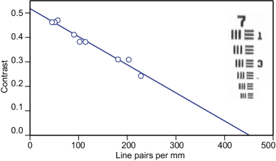
The resolution of the current imaging system is measured in four ways. First, we imaged the 1951 Air Force Test Target out of vacuum, but through an identical bucket window to the one used for the science chamber. The window was tilted at 2.5∘ to approximate the angle of the absorption beam reflected off the mirrored sample. Figure 11 shows a measurement of contrast versus line pairs/mm, from which we determine a minimum observable line width of m, and a line pair resolution of 2.2(1) m. This is 20% larger than the geometrically determined 1.8-m diffraction limit (Rayleigh-criterion) of the lens system.
We perform three in vacuo measurements. The first, shown in Fig. 12(b), is a measurement of the transverse width in of the quasi-1D BEC. The 1- width is 0.8(1) m, indicating a FWHM resolution of 1.9(1) m. Assuming a cylindrically symmetric trap, the resolution in is at least 1.9(1) m for single-shot measurements, but from knowledge of trap parameters and density, we believe the -resolution is closer to the FWHM width of the BEC, 950 nm, convolved with . (The stepping resolution the translation stage is 10 nm.)
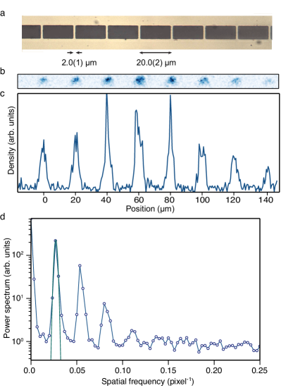
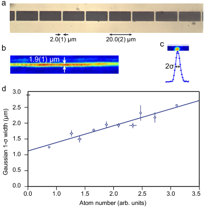
The next two methods measure the in situ resolution in . First we utilize a dimple trap formed by running current in the 2-m-wide microwire array shown in Fig. 12(a). The BEC above these sparsely spaced wires fragments into a chain of dots, the width of one of which, shown in Fig. 12(c), we measure as a function of atom number. Figure 12(d) shows the 1- radius of the dot of Bose-condensed atoms as repulsive mean field energy is reduced by trapping fewer atoms in the initial condensate. The trap population is controlled by changing the RF evaporation cooling time. Extrapolating to zero atoms, we obtain a Gaussian point-spread-function width of m, for a FWHM resolution of 2.6(2) m.
The last method, shown in Fig. 13, uses an array of 2.5-m-wide wires spaced 2.5-m apart and finds the mean 1- width of the dots of atoms in each of the microtraps. The mean 1- width is 1.0(1) m, implying a FWHM resolution of 2.4(2) m. All of these methods are consistent with one another within less than 2. We choose to take the adjusted weighted averages Paule and Mandel (1982) of the measurements to obtain the SQCRAMscope atom density and field FWHM resolvability of 2.2(1) m.
The resolvability of current sources a distance away from the in situ gas position is reduced by the convolution of the field resolvability with the field propagation transfer function, i.e., the Biot-Savart Green’s function to be described below. For a wire with transverse dimensions much smaller than , the current path resolvability is m for a BEC distance m, or 2.8(1) m at -m away.
Appendix C Field sensing calibrations
C.1 Field-to-current mapping
The mapping from measured field to inferred current distribution is performed using the procedure outlined in Ref. Roth et al. (1989) and also employed in Refs. Wildermuth et al. (2005, 2006); Della Pietra et al. (2007); Aigner et al. (2008). Using a Green’s function that accounts for the finite thickness of the source wires, the Biot-Savart mapping between field and current is
| (19) | |||||
| (20) |
where is the current density in a wire of thickness , and is the spatial wavenumber. The measured -field map taken at is first Fourier-transformed with a spatial FFT algorithm. Then, is filtered with the Green’s function effecting the Biot-Savart mapping from field-to-source current at a distance , i.e., applying Eq. 19. A Hanning window is numerically applied to the current density to remove spurious high spatial frequencies. Equation 20 yields , and finally an inverse FFT algorithm provides and .
C.2 Accuracy of extended-dynamic-range trap
We measured the accuracy, linearity, and dynamic range of the extended-dynamic-range trap in a manner similar to that presented in Fig. 3. The data are plotted in Fig. 14, where the green line is fit to the linear region and has slope 0.65(5). This implies a 3-worse accuracy than the high-sensitivity trap, possibly because it operates closer to the limit of the quasicondensate regime. As for the data in Fig. 3, we use a calibrated current source for generating the microwire current. From this slope we find that the responsivity is 35(5)% lower than the expected nT/(atom/m) for this trap.
C.3 Imaging noise
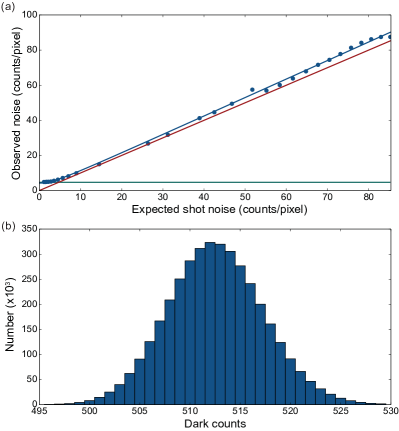
Noise contributions in the three images arise from the noise of the resonant laser beam as well as electronic readout and dark counts from the CCD camera. We measure the per-pixel noise by performing absorption imaging without atoms present. We care about the noise in a single image, and so rather than record the shot-by-shot statistics of counts in one pixel, which would include an irrelevant contribution from laser intensity noise, we use the inhomogeneous imaging light intensity across the pixel array to measure the statistics of a single-shot image. Each pixel of the image is binned by mean photon number, and the variance versus mean of the number of counts in each bin is plotted in Fig. 15a. The line of unity slope represents the photon shot-noise-limit. For short exposure times, the chilled CCD camera exhibits only 0.07 counts/pixel/s of dark count noise, but readout contributes counts/pixel during our imaging time, as measured by examining the count statistics of the dark image taken during absorption imaging; see Fig. 15(b). This readout noise dominates over shot noise below 5 counts per pixel. We observe that the imaging system is shot-noise-limited between approximately 100–3600 counts-per-pixel. The high-sensitivity trap is operated at 3000 counts-per-pixel, contributing to an equivalent field noise of 2.5(4) nT, which is consistent with the expected photon shot noise of 2.2 nT. In order to stay within the strongly saturated regime of atomic scattering, the extended-dynamic-range trap, which confines atoms at higher peak atomic density, is operated at 4500 counts-per-pixel.
C.4 Atom noise
Images of the BECs contain atomic density noise in addition to photon shot noise, and the atomic density noise can come from both shot-to-shot variance in the total trapped atom number as well as intrinsic atomic density fluctuations from position-to-position along the quasicondensate. The variance in total atom number is recorded in each shot and accurately accounted for in each run’s density–to–field mapping as long as the quasicondensate equation of state remains valid. However, the pixel-by-pixel density fluctuation does contribute to the noise floor. To eliminate the contribution of total trap population fluctuations to the measurement of the intrinsic atom density noise, we compare the pixel-by-pixel density of a single-shot image to the mean density in each pixel expected for the gas, where we define a pixel to mean the -integrated atomic density. This is accomplished by fitting the imaged density profile to a quasicondensate profile Gerbier (2004) for the same total atom number and trap parameters. This provides a mean and residual atom number for each pixel of this image, and we repeat this procedure for many such images. We then bin the means and find the residual variance for each mean. These are plotted in Fig. 16, where the black lines are the atom shot-noise limits for two imaging resolutions. The green line is the fit to the data using expressions from Ref. Gerbier (2004) for a quasicondensate. The fit allows us to measure the temperature of the gas Gerbier (2004); Jacqmin et al. (2011), which is otherwise difficult to do given the short TOF permitted by our imaging system and the small number of atoms in the thermal wings at this temperature.
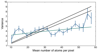
We see that the atom noise is sub-Poissonian for atom numbers-per-pixel above . The sub-shot-noise atom noise statistics are indicative of a quasicondensate, as discussed in Ref. Jacqmin et al. (2011). We operate the experiment such that the majority of pixels contain atoms in the 30–50 per-pixel range. Mean atom numbers below 10 correspond to regions of the gas not described by the quasi-1D equation of state, either because these are thermal atoms pushed out from the center of the gas in to the wings Griffin et al. (2009) and/or because this is the region in which the validity of Thomas-Fermi approximation breaks down. As such, these regions are not used for magnetometry, while numbers above 57 correspond to small regions around the centers of unusually dense BECs, leading to worse statistics in the figure. The average atom noise is 1.7(7) nT, slightly less than that from photon shot noise.
The atom shot-noise limits differ from unity slope due to the artificial averaging of fluctuations Hung et al. (2011). This is caused by the blurring due to finite imaging resolution, expansion during the short TOF, and atom diffusion arising from the random recoil imparted during imaging. The diffusion spot size is known to be accurately modeled by the diffusion equation , where is the number of photons scattered and mm/s is the recoil velocity on the imaging transition Ketterle et al. (1999). The value of is 530 nm for our parameters. This is included in the measurements of the imaging resolution. Accounting for these effects, we obtain the two shot-noise limits in Fig. 16 associated with imaging resolutions between 2.2–2.5 m.
C.5 Allan deviation
We measure the stability of the magnetometer using two methods. In Fig. 17a, we present a measurement of the Allan deviation of the minimum detectable field above the same 12-m-wide wire used for the accuracy measurements in Fig. 3 without current running in the wire. This field has a noise floor of 300 pT per pixel (no averaging) after 100 runs of the experiment, which takes roughly half an hour, though we collect information on 100 pixels during this time and thus spend less than 20 s per pixel. In the second measurement, we investigate the Allan deviation of the repeatability of the measurements of the 30-nT field created by flowing 750 nA through the 12-m wide wire with the atoms trapped 1.2-m above. The stability of the field is 1.1 nT after 30 runs. Factors that may contribute to this minimum stability level are the residual sloshing of the motion of the BEC within the trap and the drift of the position of the BEC relative to the sample.
C.6 Patch fields
Our SQCRAMscope is sensitive to other forces from the sample surface besides magnetic fields. With BECs trapped in atom chips near surfaces, Casimir-Polder forces have been detected Lin et al. (2004); Obrecht et al. (2007a) and used to determine the position of carbon nanotubes Gierling et al. (2011). Electric fields from surface charges can be detected Wildermuth et al. (2006). Such fields may arise from adsorbed Rb atoms, which can pose a difficulty for various applications McGuirk et al. (2004); Obrecht et al. (2007b); Hattermann et al. (2012); Carter et al. (2012); Chan et al. (2014); Fan et al. (2015); Thiele et al. (2015); Sedlacek et al. (2016); Naber et al. (2016). The electric field is due to an induced dipole whose magnitude varies depending on surface properties. The force increases as more atoms are absorbed onto the surface, which may occur as atoms escape the atom chip trap during loading, RF evaporation, or during TOF expansion.
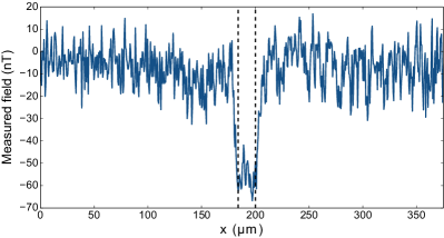
Indeed, we observe an electric force on the atoms once we have created a BEC below a particular place below the calibration chip more than a thousand times. The effects vanish once we move the BEC a few tens of microns to a fresh location. Figure 18 shows this effect after 1000 repetitions with a BEC positioned 1 m from a room-temperature, 16-m-wide gold wire. The wire is 400-nm taller than the surrounding silicon substrate, and so the electric field from the adatoms on the surface of the wire dominates that from the substrate to either side.
The electric field from the adsorbed atoms creates a local potential above the wire. This is due to several effects: 1) The closer proximity of the Au to the atoms than the Si; 2) The different polarizabilities of Rb on Au versus Si; and 3) The potentially different adhesion characteristics of Rb to Au vs Si. This potential reduces the magnetometer’s dynamic range and increases its sensitivity to sample height fluctuations. While the per-atom Rb electric dipole has been measured for several materials McGuirk et al. (2004); Obrecht et al. (2007b), we are unaware of any measurement for Au.
We do not expect this patch-field effect play a deleterious role in future SQCRAMscope magnetometry experiments because: 1) Most samples will have a smooth surface of a homogeneous material, reducing the force on the atoms from electric field gradients to a negligible level; 2) Samples can be on the mm-scale, allowing the use of fresh portions of the sample when needed; and 3) Fresh samples may be introduced with minimal downtime. Nevertheless, we can investigate the efficacy of various methods for adatom removal that have been tried by other groups, including sample heating, laser ablation and UV-light desorption McGuirk et al. (2004); Obrecht et al. (2007b); Hattermann et al. (2012); Carter et al. (2012); Chan et al. (2014); Fan et al. (2015); Thiele et al. (2015); Sedlacek et al. (2016); Naber et al. (2016).
References
- Grinolds et al. (2013) M. S. Grinolds, S. Hong, P. Maletinsky, L. Luan, M. D. Lukin, R. L. Walsworth, and A Yacoby, “Nanoscale magnetic imaging of a single electron spin under ambient conditions,” Nat. Phys. 9, 215 (2013).
- Vasyukov et al. (2013) D. Vasyukov, Y. Anahory, L. Embon, D. Halbertal, J. Cuppens, L. Neeman, A. Finkler, Y. Segev, Y. Myasoedov, M. L. Rappaport, M. E. Huber, and E. Zeldov, “A scanning superconducting quantum interference device with single electron spin sensitivity,” Nat. Nanotechnol. 8, 639 (2013).
- Kirtley et al. (2016) J. R. Kirtley, L. Paulius, A. J Rosenberg, J. C. Palmstrom, C. M. Holland, E. M. Spanton, D. Schiessl, C. L. Jermain, J. Gibbons, Y. K. K. Fung, M. E. Huber, D. C. Ralph, M. B. Ketchen, G. W. Gibson Jr., and K. A. Moler, “Scanning SQUID susceptometers with sub-micron spatial resolution,” Rev. Sci. Instrum. 87, 093702 (2016).
- Estève et al. (2004) J. Estève, C. Aussibal, T. Schumm, C. Figl, D. Mailly, I. Bouchoule, C. I. Westbrook, and A. Aspect, “Role of wire imperfections in micromagnetic traps for atoms,” Phys. Rev. A 70, 043629 (2004).
- Günther et al. (2005) A. Günther, M. Kemmler, S. Kraft, C. J. Vale, C. Zimmermann, and J. Fortágh, “Combined chips for atom optics,” Phys. Rev. A 71, 063619 (2005).
- Wildermuth et al. (2005) S. Wildermuth, S. Hofferberth, I. Lesanovsky, E. Haller, L. Mauritz Andersson, S. Groth, I. Bar-Joseph, P. Krüger, and J. Schmiedmayer, “Bose-Einstein condensates—Microscopic magnetic-field imaging,” Nature 435, 440 (2005).
- Wildermuth et al. (2006) S. Wildermuth, S. Hofferberth, I. Lesanovsky, S. Groth, P. Krüger, J. Schmiedmayer, and I. Bar-Joseph, “Sensing electric and magnetic fields with Bose-Einstein condensates,” Appl. Phys. Lett. 88, 264103 (2006).
- Aigner et al. (2008) S. Aigner, L. Della Pietra, Y. Japha, O. Entin-Wohlman, T. David, R. Salem, R. Folman, and J. Schmiedmayer, “Long-range order in electronic transport through disordered metal films,” Science 319, 1226 (2008).
- Fortágh and Zimmermann (2007) J. Fortágh and C. Zimmermann, “Magnetic microtraps for ultracold atoms,” Rev. Mod. Phys. 79, 235 (2007).
- Naides et al. (2013) M. A. Naides, R. W. Turner, R. A. Lai, J. M. DiSciacca, and B. L. Lev, “Trapping ultracold gases near cryogenic materials with rapid reconfigurability,” Appl. Phys. Lett. 103, 251112 (2013).
- Gerbier (2004) F. Gerbier, “Quasi-1D Bose-Einstein condensates in the dimensional crossover regime,” EPL 66, 771 (2004).
- Bloch et al. (2008) I. Bloch, J. Dalibard, and W. Zwerger, “Many-body physics with ultracold gases,” Rev. Mod. Phys. 80, 885–964 (2008).
- Jacqmin et al. (2011) T. Jacqmin, J. Armijo, T. Berrada, K. V. Kheruntsyan, and I. Bouchoule, “Sub-Poissonian fluctuations in a 1D Bose gas: From the quantum quasicondensate to the strongly interacting regime,” Phys. Rev. Lett. 106, 230405 (2011).
- Note (1) We actually employ the full expression given in Ref. Gerbier (2004); see also Ref. Krüger et al. (2010).
- Chu et al. (2010) J.-H. Chu, J. G. Analytis, K. De Greve, P. L. McMahon, Z. Islam, Y. Yamamoto, and I. R. Fisher, “In-plane resistivity anisotropy in an underdoped iron arsenide superconductor,” Science 329, 824 (2010).
- Bert et al. (2011) J. A. Bert, B. Kalisky, C. Bell, M. Kim, Y. Hikita, H. Y. Hwang, and K. A. Moler, “Direct imaging of the coexistence of ferromagnetism and superconductivity at the LaAlO3/SrTiO3 interface,” Nat. Phys. 7, 767 (2011).
- Qazilbash et al. (2007) M. M. Qazilbash, M. Brehm, B.-G. Chae, P. C. Ho, G. O. Andreev, B.-J. Kim, S. J. Yun, A. V. Balatsky, M. B. Maple, F. Keilmann, H.-T. Kim, and D. N. Basov, “Mott transition in VO2 revealed by infrared spectroscopy and nano-imaging,” Science 318, 1750 (2007).
- Dellabetta et al. (2012) B. Dellabetta, T. L. Hughes, M. J. Gilbert, and B. L. Lev, “Imaging topologically protected transport with quantum degenerate gases,” Phys. Rev. B 85, 205442 (2012).
- Nowack et al. (2013) K. C. Nowack, E. M. Spanton, M. Baenninger, M. König, J. R. Kirtley, B. Kalisky, C. Ames, P. Leubner, C. Brüne, H. Buhmann, L. W. Molenkamp, D. Goldhaber-Gordon, and K. A. Moler, “Imaging currents in HgTe quantum wells in the quantum spin Hall regime,” Nat. Mater. 12, 787 (2013).
- Zaanen (2016) J. Zaanen, “Electrons go with the flow in exotic material systems,” Science 351, 1026 (2016).
- Lin et al. (2004) Y.-j. Lin, I. Teper, C. Chin, and V. Vuletić, “Impact of the Casimir-Polder potential and Johnson noise on Bose-Einstein condensate stability near surfaces,” Phys. Rev. Lett. 92, 050404 (2004).
- Obrecht et al. (2007a) J. M. Obrecht, R. J. Wild, M. Antezza, L. P. Pitaevskii, S. Stringari, and E. A. Cornell, “Measurement of the temperature dependence of the Casimir-Polder force,” Phys. Rev. Lett. 98, 063201 (2007a).
- Kirtley et al. (2012) J. R. Kirtley, B. Kalisky, J. A. Bert, C. Bell, M. Kim, Y. Hikita, H. Y. Hwang, J. H. Ngai, Y. Segal, F. J. Walker, C. H. Ahn, and K. A. Moler, “Scanning SQUID susceptometry of a paramagnetic superconductor,” Phys. Rev. B 85, 224518 (2012).
- Iranmanesh et al. (2014) M. Iranmanesh, M. Stir, J. R. Kirtley, and J. Hulliger, “Scanning SQUID microscopy of local superconductivity in inhomogeneous combinatorial ceramics,” Chem. Eur. J. 20, 15816 (2014).
- Pham et al. (2011) L. M. Pham, D. Le Sage, P. L. Stanwix, T. K. Yeung, D. Glenn, A. Trifonov, P. Cappellaro, P. R. Hemmer, M. D. Lukin, H. Park, A. Yacoby, and R. L. Walsworth, “Magnetic field imaging with nitrogen-vacancy ensembles,” New J. Phys. 13, 045021 (2011).
- Shields et al. (2015) B. J. Shields, Q. P. Unterreithmeier, N. P. de Leon, H. Park, and M. D. Lukin, “Efficient readout of a single spin state in diamond via spin-to-charge conversion,” Phys. Rev. Lett. 114, 136402 (2015).
- Lovchinsky et al. (2016) I. Lovchinsky, A. O. Sushkov, E. Urbach, N. P. de Leon, S. Choi, K. De Greve, R. Evans, R. Gertner, E. Bersin, C. Müller, L. McGuinness, F. Jelezko, R. L. Walsworth, H. Park, and M. D. Lukin, “Nuclear magnetic resonance detection and spectroscopy of single proteins using quantum logic,” Science 351, 836 (2016).
- Vengalattore et al. (2007) M. Vengalattore, J. M. Higbie, S. R. Leslie, J. Guzman, L. E. Sadler, and D. M. Stamper-Kurn, “High-resolution magnetometry with a spinor Bose-Einstein condensate,” Phys. Rev. Lett. 98, 200801 (2007).
- Brook et al. (2003) A. J. Brook, S. J. Bending, J. Pinto, A. Oral, D. Ritchie, H. Beere, M. Henini, and A. Springthorpe, “Integrated piezoresistive sensors for atomic force-guided scanning Hall probe microscopy,” Appl. Phys. Lett. 82, 3538 (2003).
- Nirrengarten et al. (2006) T. Nirrengarten, A. Qarry, C. Roux, A. Emmert, G. Nogues, M. Brune, J. M. Raimond, and S. Haroche, “Realization of a superconducting atom chip,” Phys. Rev. Lett. 97, 200405 (2006).
- Mukai et al. (2007) T. Mukai, C. Hufnagel, A. Kasper, T. Meno, A. Tsukada, K. Semba, and F. Shimizu, “Persistent supercurrent atom chip,” Phys. Rev. Lett. 98, 260407 (2007).
- Roux et al. (2008) C. Roux, A. Emmert, A. Lupascu, T. Nirrengarten, G. Nogues, M. Brune, J. M. Raimond, and S Haroche, “Bose-Einstein condensation on a superconducting atom chip,” EPL 81, 56004 (2008).
- Müller et al. (2010) T. Müller, B. Zhang, R. Fermani, K. S. Chan, Z. W. Wang, C. B. Zhang, M. J. Lim, and R. Dumke, “Trapping of ultra-cold atoms with the magnetic field of vortices in a thin-film superconducting micro-structure,” New J. Phys. 12, 043016 (2010).
- Reichel and Vuletic (2010) J. Reichel and V. Vuletic, Atom Chips (Wiley, 2010).
- Cano et al. (2008) D Cano, B Kasch, H Hattermann, R Kleiner, C Zimmermann, D Koelle, and J Fortágh, “Meissner Effect in Superconducting Microtraps,” Phys. Rev. Lett. 101, 183006–4 (2008).
- Jessen et al. (2013) F. Jessen, M. Knufinke, S. C. Bell, P. Vergien, H. Hattermann, P. Weiss, M. Rudolph, M. Reinschmidt, K. Meyer, T. Gaber, D. Cano, A. Günther, S. Bernon, D. Koelle, R. Kleiner, and J. Fortágh, “Trapping of ultracold atoms in a 3He/4He dilution refrigerator,” Appl. Phys. B 116, 665 (2013).
- Minniberger et al. (2014) S. Minniberger, F. Diorico, S. Haslinger, C. Hufnagel, C. Novotny, N. Lippok, J. Majer, C. Koller, S. Schneider, and J. Schmiedmayer, “Magnetic conveyor belt transport of ultracold atoms to a superconducting atomchip,” Appl. Phys. B 116, 1017 (2014).
- Chan et al. (2014) K. S. Chan, M. Siercke, C. Hufnagel, and R. Dumke, “Adsorbate electric fields on a cryogenic atom chip,” Phys. Rev. Lett. 112, 026101 (2014).
- Rugar et al. (2004) D. Rugar, R. Budakian, H. J. Mamin, and B. W. Chui, “Single spin detection by magnetic resonance force microscopy,” Nature 430, 329 (2004).
- Ockeloen et al. (2013) C. F. Ockeloen, R. Schmied, M. F. Riedel, and P. Treutlein, “Quantum metrology with a scanning probe atom interferometer,” Phys. Rev. Lett. 111, 143001 (2013).
- Wildermuth (2005) S. Wildermuth, One-dimensional Bose-Einstein condensates in micro-traps, Ph.D. thesis, U. Heidelberg (2005).
- Aigner (2007) S. Aigner, Magnetic Field Microscopy using Ultracold Atoms, Ph.D. thesis, U. Heidelberg (2007).
- Pelliccione et al. (2016) M. Pelliccione, A. Jenkins, P. Ovartchaiyapong, C. Reetz, E. Emmanouilidou, N. Ni, and A. C. Bleszynski Jayich, “Scanned probe imaging of nanoscale magnetism at cryogenic temperatures with a single-spin quantum sensor,” Nat. Nanotechnol. 11, 700 (2016).
- Taylor et al. (2008) J. M. Taylor, P. Cappellaro, L. Childress, L. Jiang, D. Budker, P. R. Hemmer, A. Yacoby, R. Walsworth, and M. D. Lukin, “High-sensitivity diamond magnetometer with nanoscale resolution,” Nat. Phys. 4, 810 (2008).
- Treutlein et al. (2004) P. Treutlein, P. Hommelhoff, T. Steinmetz, T. W. Hänsch, and J. Reichel, “Coherence in microchip traps,” Phys. Rev. Lett. 92, 203005 (2004).
- Berg et al. (2007) E. Berg, E. Fradkin, E. A. Kim, S. A. Kivelson, V. Oganesyan, J. M. Tranquada, and S. C. Zhang, “Dynamical layer decoupling in a stripe-ordered high- superconductor,” Phys. Rev. Lett. 99, 127003 (2007).
- Berg et al. (2009) E. Berg, E. Fradkin, and S. A. Kivelson, “Theory of the striped superconductor,” Phys. Rev. B 79, 064515 (2009).
- Kivelson (2016) S. Kivelson, (2016), private communication.
- Ketterle et al. (1999) W. Ketterle, D. S. Durfee, and D. M. Stamper-Kurn, “Making, probing and understanding Bose-Einstein condensates,” in Proceeedings of the International School of Physics “Enrico Fermi,” course CXL, edited by M. Inguscio, S. Stringari, and C. E. Wieman (IOS) (Press, 1999) p. 67.
- Smith et al. (2011) D. A. Smith, S. Aigner, S. Hofferberth, M. Gring, M. Andersson, S. Wildermuth, P. Krüger, S. Schneider, T. Schumm, and J. Schmiedmayer, “Absorption imaging of ultracold atoms on atom chips,” Opt. Express 19, 8471 (2011).
- Reinaudi et al. (2007) G. Reinaudi, T. Lahaye, .Z Wang, and D. Guéry-Odelin, “Strong saturation absorption imaging of dense clouds of ultracold atoms,” Opt. Lett. 32, 3143 (2007).
- Paule and Mandel (1982) R. C. Paule and J. Mandel, “Consensus values and weighting factors,” J. Res. Nat. Bur. Stand 87, 377 (1982).
- Roth et al. (1989) B. J. Roth, N. G. Sepulveda, and J. P. Wikswo Jr., “Using a magnetometer to image a two-dimensional current distribution,” J. Appl. Phys. 65, 361 (1989).
- Della Pietra et al. (2007) L. Della Pietra, S. Aigner, C. vom Hagen, S. Groth, I. Bar-Joseph, H. J. Lezec, and J. Schmiedmayer, “Designing potentials by sculpturing wires,” Phys. Rev. A 75, 063604 (2007).
- Griffin et al. (2009) A. Griffin, T. Nikuni, and E. Zaremba, Bose-Condensed Gases at Finite Temperatures (Cambridge University Press, 2009).
- Hung et al. (2011) C.-L. Hung, X. Zhang, L.-C. Ha, S.-K. Tung, N. Gemelke, and C. Chin, “Extracting density–density correlations from in situ images of atomic quantum gases,” New J. Phys. 13, 075019 (2011).
- Gierling et al. (2011) M. Gierling, P. Schneeweiss, G. Visanescu, P. Federsel, M. Häffner, D. P. Kern, T. E. Judd, A. Günther, and J. Fortágh, “Cold-atom scanning probe microscopy,” Nat. Nanotechnol. 6, 446 (2011).
- McGuirk et al. (2004) J. M. McGuirk, D. M. Harber, J. M. Obrecht, and E. A. Cornell, “Alkali-metal adsorbate polarization on conducting and insulating surfaces probed with bose-einstein condensates,” Phys. Rev. A 69, 062905 (2004).
- Obrecht et al. (2007b) J. M. Obrecht, R. J. Wild, and E. A. Cornell, “Measuring electric fields from surface contaminants with neutral atoms,” Phys. Rev. A 75, 062903 (2007b).
- Hattermann et al. (2012) H. Hattermann, M. Mack, F. Karlewski, F. Jessen, D. Cano, and J. Fortágh, “Detrimental adsorbate fields in experiments with cold Rydberg gases near surfaces,” Phys. Rev. A 86, 022511 (2012).
- Carter et al. (2012) J. D. Carter, O. Cherry, and J. D. D. Martin, “Electric-field sensing near the surface microstructure of an atom chip using cold Rydberg atoms,” Phys. Rev. A 86, 053401 (2012).
- Fan et al. (2015) H. Fan, S. Kumar, J. Sedlacek, H. Kübler, S. Karimkashi, and J. P. Shaffer, “Atom based RF electric field sensing,” J. Phys. B 48, 202001 (2015).
- Thiele et al. (2015) T. Thiele, J. Deiglmayr, M. Stammeier, J. A. Agner, H. Schmutz, F. Merkt, and A. Wallraff, “Imaging electric fields in the vicinity of cryogenic surfaces using Rydberg atoms,” Phys. Rev. A 92, 063425 (2015).
- Sedlacek et al. (2016) J. A. Sedlacek, E. Kim, S. T. Rittenhouse, P. F. Weck, H. R. Sadeghpour, and J. P. Shaffer, “Electric field cancellation on quartz by Rb adsorbate-induced negative electron affinity,” Phys. Rev. Lett. 116, 133201 (2016).
- Naber et al. (2016) J. Naber, S. Machluf, L. Torralbo-Campo, M. L. Soudijn, N. J. van Druten, H. B. van Linden van den Heuvell, and R. J. C. Spreeuw, “Adsorbate dynamics on a silica-coated gold surface measured by Rydberg Stark spectroscopy,” J. Phys. B 49, 094005 (2016).
- Krüger et al. (2010) P. Krüger, S. Hofferberth, I. E. Mazets, I. Lesanovsky, and J. Schmiedmayer, “Weakly interacting Bose gas in the one-dimensional limit,” Phys. Rev. Lett. 105, 265302 (2010).