Apparent rippling with honeycomb symmetry and tunable periodicity observed by scanning tunneling microscopy on suspended graphene
Abstract
Suspended graphene is difficult to image by scanning probe microscopy due to the inherent van-der-Waals and dielectric forces exerted by the tip which are not counteracted by a substrate. Here, we report scanning tunneling microscopy data of suspended monolayer graphene in constant-current mode revealing a surprising honeycomb structure with amplitude of 50200 pm and lattice constant of 10-40 nm. The apparent lattice constant is reduced by increasing the tunneling current , but does not depend systematically on tunneling voltage or scan speed . The honeycomb lattice of the rippling is aligned with the atomic structure observed on supported areas, while no atomic corrugation is found on suspended areas down to the resolution of about pm. We rule out that the honeycomb structure is induced by the feedback loop using a changing , that it is a simple enlargement effect of the atomic lattice as well as models predicting frozen phonons or standing phonon waves induced by the tunneling current. Albeit we currently do not have a convincing explanation for the observed effect, we expect that our intriguing results will inspire further research related to suspended graphene.
I Introduction
Two-dimensional (2D) materials such as graphene can be stabilized by an anharmonic coupling of in-plane and out-of plane phonons leading to a rippled 2D layer.Katsnelson
Transmission electron microscopy (TEM) probing the suspended areas of partly supported graphene has found such a rippling on length scales of about 10 nm with amplitudes of about 1 nm by analyzing the tilt dependence of local diffraction patterns.Meyer The length scales are in nice agreement with predictions from molecular dynamics (MD) simulations for freely suspended graphene.Vozmedanio Experimentally, rippling can also be induced by the substrate,Ishigami ; Stolyarova ; Cullen by a non-conformal transfer of graphene onto a support material,Geringer ; Mashoff ; Morgenstern ; Calado ; Lanza by heating and cooling Bao ; Tapaszto ; Bai due to the negative thermal expansion coefficient of graphene,NTA
by compressive edge stress,Shenoy or by stress around defects.Warner This has been recently reviewed in detail.Deng
Probing the detailed topography of the rippling on suspended graphene is difficult. TEM suffers from a low contrast of monolayer graphene and its intrinsic low sensitivity to the vertical displacements,Meyer2 ; Wang ; Warner ; Bangert while scanning probe microscopy modifies the structure due to the attractive van-der-Waals force exerted onto the graphene by the tip, which can be accompanied by attractive dielectric forces depending on the local tip potential.Mashoff ; Stroscio ; Xu1 This leads to a strong pulling of the graphene membrane by the tip, e.g., within constant-current mode imaging by a scanning tunneling microscope (STM). The pulling height was measured to be about nm on suspended areas, if the tip is m apart from the support.Stroscio ; Xu1 Resulting lateral modifications of the graphene morphology by the tip forces have been observed rather directly within a dual tip STM.Eder
Nevertheless, interesting effects have been found using STM on suspended graphene. For example, the tip forces induce an inhomogeneous pseudomagnetic field of about 10 T directly below the tip.Stroscio ; Stroscio1 This leads to confinement of electronic states, which exhibit Coulomb blockade and orbital splittings in tunneling transport.Stroscio
Atomic resolution and static ripples of 5-10 nm length scale have also been observed in suspended areas, if measured slowly and on small length scales.Zan ; Stroscio ; Xu1 ; Zhao
In some experiments, it has been found that the amplitude of the atomic corrugation depends on scan speed and can be up to 1 nm, much larger than for supported samples.Xu1
Moreover, the membrane retracts by up to 20 nm while increasing the current, which is claimed to be related to local heating,Xu2 albeit quantitatively not compatible with the large heat conductivity of graphene (see below).Pop Time series in constant current mode revealed a current dependence of the sub-Hz-frequency spectrum of the vertical tip movement Xu3 as well as occasional jumps up to 40 nm attributed to unbuckling processes of the membrane.Neek
These results have recently been described by two power laws distinguishing vibrational motion and unbuckling processes.Peeters
Here, we report a surprising effect that we observed occasionally on suspended graphene, namely an apparent rippling with honeycomb symmetry, aligned with the atomic lattice as observed on the supported areas, but with much larger period. Keeping the tunneling current constant, the rippling pattern is reproducibly observed on the identical area independently on scan speed or scan direction of the tip. Furthermore, the period is increased from 10 nm to 40 nm by decreasing the tunneling current from 500 pA to 100 pA.
The effect has not been reported in previous publications, maybe since these experiments are mostly performed on smaller membranes with diameters of 1 m only and provide much smaller STM image sizes below nm2.Stroscio ; Stroscio1 ; Zan ; Xu1 ; Xu2 ; Neek ; Zhao
Excluding several possible explanations, we could not come up with a convincing description of the apparent rippling, thus, hoping to stimulate further successful theoretical work.
II Experiment
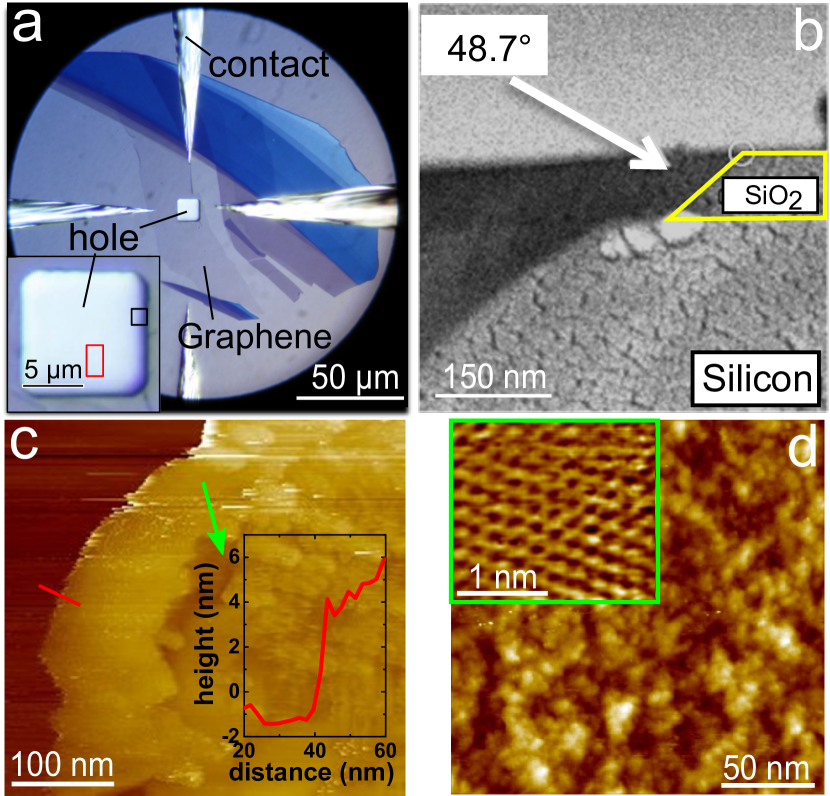
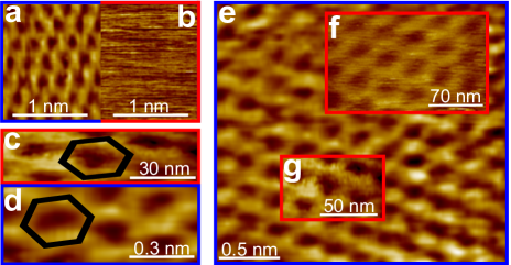
Graphene is exfoliated on 90 nm thick SiO2 on Si(001) using adhesive tape.Novoselov The substrate includes rectangular holes (m2) fabricated by reactive ion etching. By chance, a monolayer of graphene was deposited partly on such a hole (Fig. 1a), i.e., it is suspended across m2. The hole edge exhibits a declining slope of with respect to the surface due to the etching process (Fig. 1b). Atomic force microscopy (AFM) reveals additionally that some sections of the rim exhibit an outer area with a slope of only . Previous AFM measurements found that the graphene sticks to the edges of such holes.Lee2008 Thereby it gains adhesion energy while being increasingly strained before eventually getting fully suspended within the center of large enough holes. The largest part of our graphene flake (Fig. 1a) resides on the substrate fully encircling the suspended area. At its edges, it is surrounded by thicker graphite areas (dark blue areas in Fig. 1a) .
Raman spectroscopy is used to verify that the suspended graphene is a monolayer.Ferrari Afterwards, the graphene is electrically contacted by microsoldering with indium while at C in ambient environment.Girit ; Geringer2
After transfering into a home-built ultrahigh vacuum STM operating at a temperature of K, the STM tip was aligned to the graphene flake using an optical microscope with a focal range up to 20 cm and a resolution of m Geringer2 . During this process, the clearly visible In leads act as additional cross hairs. The tip approach is then performed on the supported areas in order to avoid destruction of the suspended areas by tip forces. Afterwards we manoeuvered the tip to the suspended areas without loosing tunneling current. Later, we also approached on the suspended areas, but starting from smaller tip-sample distances.
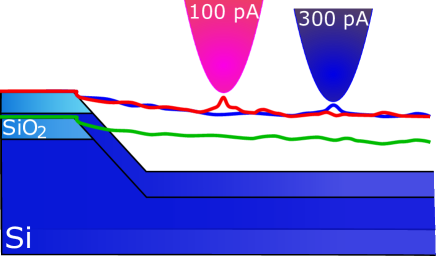
STM images were measured in constant-current mode at scan speed , current , and sample voltage . In order to avoid dielectric forces during imaging we operate at mV close to the contact potential. This compensates work function differences between tip and sample. The contact potential can be determined by relating curves on suspended and supported areas as described elsewhere.Mashoff curves (: vertical distance of tip) are recorded with feedback off after stabilizing the tip at current and voltage .
III Results
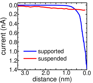
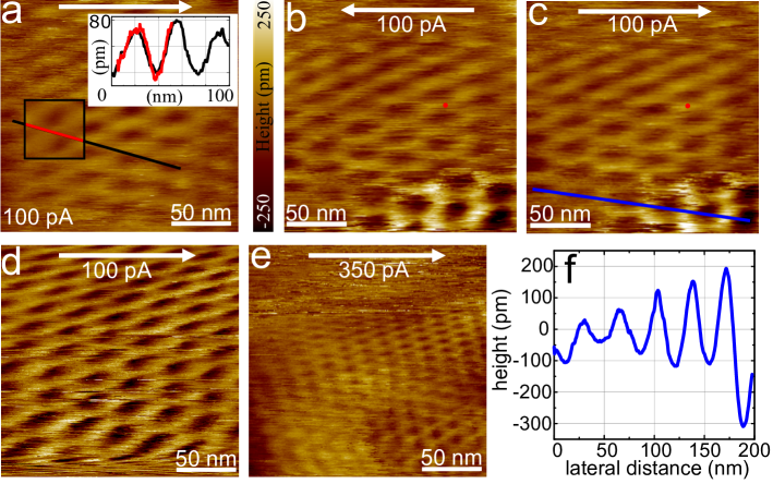
Figure 1a shows an optical image of the graphene flake completely covering the marker hole.
The colored frames in the inset mark the areas where STM measurements have been pursued. The slope of the marker hole is mostly about 50∘ (Fig. 1b), while the slope of the graphene as measured by STM on the suspended regions is typically 4∘ revealing that the graphene is indeed suspended above the marker hole. Figure 1c shows an STM image obtained close to the edge of the marker hole while scanning from left to right. It exhibits a sharp step of 4 nm height.
On the right side of the step, the graphene appears relatively flat (rms roughness: nm on 50 nm length scales, nm on larger length scales) until we observe an additional hole-like area (green arrow) followed by an area of stronger corrugation also on smaller length scales (rms roughness: nm). The later value of is much larger than the roughness observed far away from the marker hole edge. The latter is nm (Fig. 1d) being in good agreement with earlier results of graphene on SiO2.Geringer ; Cullen ; Stolyarova ; Ishigami The large roughness is most likely induced by a rougher substrate around the marker hole caused by the etching process. The sharp step is not observed while scanning from right to left, while the area to the right of the step is imaged identically (not shown). We assume that the step marks an abrupt delaminating of the graphene from the edges of the hole due to the attractive van-der-Waals forces of the tip, while the increased corrugation marks the onset of supported graphene.
Most importantly, the transition from supported to suspended graphene as marked by the green arrow can be determined with a precision of, at least, 100 nm.
A much weaker decay of curves is observed on the suspended areas (Fig. 2). The current decays nearly linearly by about 25 pA/nm starting from 100 pA at closest distance. This indicates that the membrane is pulled with the tip (see below). We find featureless curves on both areas with minima around mV (not shown).
Figure 1d shows STM images on the supported areas. They are recorded more than 1 m away from the edge of the marker hole. They exhibit the well known rippling of graphene down to 10 nm length scales with an rms roughness of 0.25 nm.Geringer ; Cullen ; Stolyarova ; Ishigami Atomic resolution with the typical honeycomb lattice and a corrugation of about pm is observed on smaller length scales (inset).
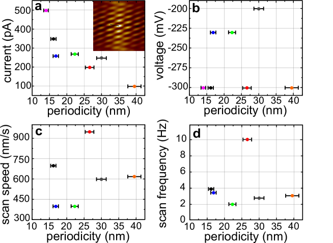
Figure 3 shows STM images obtained on the suspended areas more than 1 m away from the edges of the marker hole. STM images recorded closer to the edge exhibit rather irregular structures and are quite unstable, i.e. the image appearance changes rapidly during scanning. But far away from the edges, we reproducibly observe a regular honeycomb structure.
Figure 3a-c show subsequently obtained images on the same area revealing the reproducibility of the pattern. The inset enframed in black in Fig. 3a is a zoom into that area recorded at much smaller revealing that the pattern is rather exactly reproduced independent of , if tip, and are not changed (see also profile lines in the upper inset). Also the direction of scanning does not change the pattern except minor details (Fig. 3b and c). We find a small relative offset of the patterns in the fast scan direction of about 10 nm, but no offset in the slow scan direction. An offset of nm in the fast scan direction is also observed on supported areas using the same image size and the same nm/s and is traced back to the piezo creep of the tube scanner. Thus, most of the offset between Fig. 3b and c is due to creep, but there might be an additional offset due to lateral drag of the graphene membrane by the tip of about 5 nm.
Finally, retracting the tip from the membrane in -direction by more than 100 nm, thereby, completely loosing the tunneling current, and reapproaching, does barely changes the observed pattern. Figure 3d shows an image of the same area as recorded in Fig. 3ac after such a new approach.
The fact that the very same tip revealed reasonable corrugation and atomic resolution images on supported areas (Fig. 1d) prior, in between, and after the imaging of the large scale corrugation on the suspended areas excludes that the observed pattern is an artifact of the measurement equipment. We also carefully checked the error signal of the feedback loop being typically below 2 % during imaging of the structures in Fig. 3. Moreover, the tube scanner did not operate in its extreme positions during the imaging. Thus, we conclude that the observed patterns represent the real -movement of the tunneling tip in constant-current mode, exhibiting a large scale corrugation with honeycomb symmetry.
The amplitude of the corrugation is changing within an image and also in between images by up to a factor of three (see e.g. line scan in Fig. 3f) without any systematic dependence on measurement parameters. We believe that it is related to details of the tip shape, which are known to rapidly change at room temperature.
Most surprisingly, the periodicity of the apparent honeycomb lattice changes dramatically, if the tunneling current is changed. Figure 3e is measured on the identical area as Fig. 3ad, but at a current of pA instead of pA, while maintaining and . The period of the honeycomb lattice decreases from 40 nm to about 15 nm, while the amplitude barely changes being on average 100 pm at pA and 150 pm at pA.
Figure 4 shows this trend quantitatively for images recorded at slightly different positions within the red rectangle of the inset of Fig. 1a. For these images, also and are slightly changed. The periodicity is deduced using autocorrelation maps of the constant current images as shown in the inset of Fig. 4a. It is chosen as the distance between the central peak and the neighboring peaks closest to the direction of fast scanning (black line in inset of Fig. 4a). These peaks are selected, since they are the least influenced by thermal drift or piezocreep. A clear trend of increasing period of the honeycomb lattice with decreasing current is found (Fig. 4a), but no systematic dependence on voltage, scan speed, or scan frequency, i.e. the number of lines recorded per second (Fig. 4bd, see also Fig. 3a for a more extreme case of changing ). The amplitude of the honeycomb corrugation varies between 50 pm and 200 pm, but again without a trend with respect to , , and .
Interestingly, the orientation of the long-range corrugation is quite similar to the orientation of the atomic lattice observed on supported areas with the same tip. In addition, the suspended areas do not exhibit atomic resolution. These results are emphasized in Fig. 5. Figure 5a and b compare STM images on supported and suspended areas using the same lateral magnification and the same color scale for the height information. While an obvious honeycomb lattice with the period expected from the atomic lattice of graphene is visible on the supported areas (corrugation amplitude: 30 pm), there is no honeycomb pattern apparent on the suspended areas down to the noise level of 5 pm. Even after removing the noise by adequate filtering we do not observe any signs of an atomic scale honeycomb pattern, such that we can exclude it down to amplitudes of 34 pm. Figure 5c and d compare the large scale corrugation on suspended areas (c) with the atomic resolution on supported areas (d) by adjusting the magnification and the height contrast. The patterns are quite similar albeit the long range corrugation appears more strongly distorted, i.e. the lattice constant in horizontal direction is significantly larger than in vertical direction. If we symmetrize the honeycomb structure on suspended areas by stretching the images vertically, in order to compensate for likely effects of thermal drift, remaining piezocreep or drag, and overlap the resulting images (Fig. 5f and g) on an atomic resolution image (Fig. 5e), the similarity becomes even more striking.
IV Discussion
Albeit, we do not have an explanation for the observed effect, we will present the arguments against the most obvious possible scenarios.
IV.1 Instrumental artifacts
First, we should exclude that the observed corrugation is an artifact of the measurement equipment, i.e., we simply measure the atomic corrugation on the wrong lateral scale. Such a scenario appears appealing since other authors find atomic resolution on suspended graphene with relatively large amplitudes of 0.11 nm.Zan ; Stroscio ; Xu1 ; Zhao These amplitudes are similar to the amplitudes of our large scale corrugation. However, firstly we observed the large scale corrugation with different microtips (up to 3 month in between) on different areas of the suspended region, e.g., within the red rectangle but also at the left edge of the black rectangle of the inset of Fig. 1a. Moreover, we find it reproducibly prior and after moving to the substrate area, where we obtain normal STM images of graphene with atomic resolution as in Fig. 1d. We also took care that the tube scanner has operated in its intermediate low voltage position with respect to movement and movement. Coming from the substrate, we had to follow a 4∘ downwards slope towards the center of the membrane indicating a remaining attraction of the graphene by the substrate most likely of van-der Waals type. Thus, the tube scanner has been extended by about 200 nm for the measurements on the membrane, still being well apart from the maximum extraction of 600 nm. Indeed, the tip was only extracted by nm with respect to its equilibrium position during all measurements on the membrane. Thus, we can safely exclude a wrong operation of our instrument exclusively on the suspended areas.
IV.2 Model of the membrane during tunneling
In order to discuss further possible explanations of the found apparent rippling, we need a description of the membrane during tunneling. Our model is sketched in Fig. 6. It is largely based on previous, partly coarse grained MD simulations of a freely suspended membrane in presence of a tip.Mashoff ; Stroscio ; Stroscio1 ; Nemes These calculations revealed, that an Ir sphere (representing the tip) on top of a graphene membrane without a substrate below, but with a counteracting gate force, leads to a Gaussian bump within the graphene directly below the tip. The bump is surrounded by a concave shape of the membrane.Stroscio ; Stroscio1 Below, we argue that the intrinsic rippling of the membrane is barely changed by the tip forces. We sketch this situation by the red and blue line in Fig. 6. According to the experiments, we have to assume that the stretched area gets pulled with the tip, while lowering , which is displayed by the difference between red and blue line.
We now describe the arguments leading to Fig. 6 in detail.
Firstly, the fact, that the tip used on the membrane reveals an exponential increase of the tunneling current up to nA on supported areas (Fig. 2), implies that we operate in tunneling distance at nA on suspended areas, too.
It excludes, in particular, the presence of an oxide barrier at the front of the tip, which would lead to tunneling even if tip and graphene are in contact, but would result in a saturation of .
It is very unlikely that the resistance of the graphene membrane itself increases up to 1-2 G at 300 K due to stretching by the tip, while the tip is in ohmic contact with the membrane. In particular, such a high membrane resistance would lead to instabilities of the transport due to local charging by the tip electrons,Bindel which was not observed in the experiment in agreement with earlier results.Stroscio
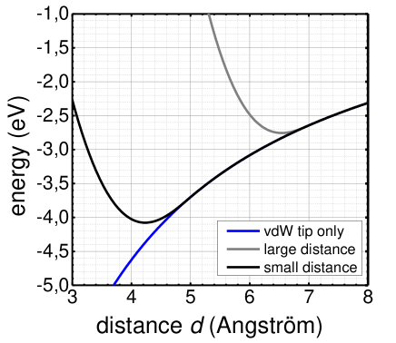
In favor of the tunneling model without contact, one can easily show that the graphene membrane can reside in an energy minimum at tunneling distance of Å. One firstly estimates the van-der-Waals energy between tip and graphene by the Hamaker approximation. We use a sphere with radius as tip in distance above a plane representing the graphene,Israel
which reveals for :
| (1) |
The required parameters to calculate the coefficient and the atomic densities and of the W tip and graphene, respectively, are taken from the literature.parameters
A sphere of nm matches the strength of the van-der-Waals energies revealed from MD simulations within the LAMMPS code,LAMMPS thereby, using a W pyramid with (110) axis as tip. With this sphere, we obtain eVÅ/ [Å].
There are a number of possible errors in this estimate. Firstly, the experimentally based Hamaker constants between graphene and W vary by up to a factor of two.parameters Secondly, the tip radius could be different. It is bound by the fact that we observe atomic resolution, i.e., nm, but we cannot exclude that the tip is effectively sharper than the W pyramid leading to an effective radius down to nm. This reveals another factor of 2.5 of possibly larger van-der-Waals interactions. Thirdly, the model neglects details of the change of the polarizibility functions by the atomic environment.Tkatchenko1 The adapted values result on the one hand from polarizability measurements of a W tip parameters which should mimic the experimental situation well. On the other hand, the used values for C origin from Hartree-Fock calculations of Graphite adsorption energies parameters and, thus, might also be close to the experimental ones. Corresponding errors are probably in the range of several 10 %. Fourthly, screening is neglected, which reduces the van-der-Waals forces, again in the range of a few 10 %.Tkatchenko2 Fifthly, Casimir-Polder forces caused by retardation are neglected, but they start to be of relevance at distances of more than 10 nm between the interacting materials only.Israel ; Casimir Finally and most importantly, long-range excitations can lead to an even qualitatively different behavior. The interaction can be significantly enhanced and has been found theoretically to vary by up to a factor of seven between different C structures notably exhibiting the largest effective, atomic value for graphene. Tkatchenko3 An increase of atomic values for C based molecules with molecular size by up to 20 % is found experimentally, which confirms such a scenario.Tautz Density functional theory based calculations even predict that decay exponents are changed due to the long range excitations, e.g. two graphene layers at about 1 nm distance exhibit an exponent of instead of .Ambrosetti
Unfortunately, accurate AFM measurements of force-distance curves absorb varying exponents in the unknown shape of the tip apex.AFM
Thus, without detailed calculations, the resulting error can barely be estimated. However, due to the fact that our parameters are based on experimental values of a W tip and Hartree-Fock calculations of graphite make us confident that the corresponding error is not too large. So, we expect errors in the van-der-Waals forces between tip and graphene by up to a factor of five, which is the largest error in all the estimated forces in this manuscript.
The elastic strain energy within the graphene membrane due to stretching by the tip forces is also estimated by LAMMPS calculations. Therefore, we simulate graphene on
SiO2 in presence of the pyramidal W tip. We use the adaptive imtermolecular reactive bond order (AIREBO) potential for the interatomic forces in graphene.AIREBO It is crosschecked by continuum plate mechanics calculations using the known Lam parameters of graphene.Lame
The calculations confirm that the pyramidal W-tip induces a Gaussian bump within the graphene directly below the tip (even on the substrate).
This bump exhibits a -width of 5-7 Å.Nemes
A similar width of the Gaussian within the concave areas has been found by MD simulations of a free membrane in presence of a tip.Stroscio ; Stroscio1
The corresponding strain energy as a function of the height of the Gaussian is well fitted by [Å]2.7 for typical Å.
It is now straightforward to determine the potential energy for different as shown in Fig. 7. We find pronounced metastable minima, e.g., at Å or Å. The energy barrier towards the global minimum, where the graphene is attached to the tip, amounts to 10 eV and 60 eV, respectively. Consequently, the tunneling position is quite stable even at room temperature and even considering the large error bar of the tip-graphene van-der Waals forces.
We conclude that the huge elastic modulus of graphene ( N/m)Lee2008 allows stable tunneling on suspended graphene, which in turn requires that the membrane below the tip is stretched during tunneling. Corresponding maximum strains amount to about 1 % according to the MD simulations.Nemes ; Stroscio ; Stroscio1
Notice that the equilibrium graphene-tip distance in Fig. 7 changes by Å , when changes by only 2 Å. This implies for the experiment, that the membrane moves towards the tip by 0.3 Å, when the tip is approaching by 2 Å, such that the curve on the membrane must be steeper than on supported areas.Mashoff This is in obvious contrast to the experiment in Fig. 2 and will be discussed below.
Secondly, we discuss the van-der-Waals forces of the substrate. The Si substrate is at a distance of m below the membrane as determined by AFM. The energy density of its interaction with the graphene can be estimatedIsrael using with taken from the literature,parameters revealing meV/m2. Thus, is irrelevant with respect to and . The resulting total van-der-Waals energy across the membrane of eV leads to minimal stretching of flat graphene. The strain amounts to less than 1 Å across the 10 m of the membrane. However, in case that the membrane is larger than the hole, e.g., due to the heat treatment during sample preparation,NTA the membrane could be bent downwards to the substrate due to the size mismatch and . We believe that this explains the about downwards movement of the tip towards the center of the membrane.
Notice that the thermal energy of the out-of plane movement of the graphene, being close to meV/atom (: Boltzmann constant) at room temperature,ZPA is much larger than . Consequently, the graphene will be additionally dynamically rippled.Vozmedanio
The tip will easily pull the graphene upwards against . However, since the tip has typically a conical shape on larger scales with angles of about with respect to the axis of the tip wire, there will be large areas of the suspended graphene where the substrate is closer to the graphene than any tip area (see Fig. 6). Thus, we expect that the graphene still globally hangs downwards, while only pulled upwards within an area of about m2 below the tip. This explains that we have to move downwards by about towards the center of the membrane.
Of course, there are also errors in the determination of the van-der-Waals forces between graphene and the substrate. However, since the parameters are matched to experiments, they are probably not too large, such that the general conclusions are not modified.
Thirdly, the thermal energy density of the out-of plane movement of the graphene is larger than the van-der Waals energy density provided by the tip, if the tip atoms are more than 5 nm apart from the graphene (see eq.1). Thus, only a very small area of the graphene directly below the tip apex will be smoothed and stretched by . We note in passing that previous MD simulations at K using a sphere for the representation of the tip found that only the inner 20 nm below the tip exhibit an inhomogeneous strain. This result was independent of the size of the sphere and the size of the membrane, if larger in radius than 20 nm or 200 nm, respectively. Thus, the exerted strain by the tip will appear on a rather reduced lateral size only.
Fourthly, we find experimentally that decays much weaker on suspended areas than on supported areas (Fig. 2).
This contradicts the one-dimensional model displayed in Fig. 7. There, an increased distance between tip and graphene results in reduced , which implies a retraction of the membrane due to the unchanged retracting . This would inevitably lead to a stronger decay of with vertical tip position than for a graphene layer fixed to the substrate, as observed, e.g., while lifting originally supported graphene.Mashoff
However, the van-der-Waals forces of the tip are strongly inhomogeneous in the tip area. One could imagine that the curvature of the Gaussian bump changes while retracting the tip. Consequently, the Gaussian gets smaller, and,thus, counterintuitively, the tunneling atom of the graphene could be moved towards the direction of the retracting tip. The low bending rigidity of graphene ( eV according to theoryWei in agreement with experimentTapaszto ) allows such a behavior in principle. We found a hint towards such a behavior by MD calculations of graphene on a SiO2 substrate. The width of the pulled-up Gaussian indeed decreases from 7 Å to 6 Å , if the tip is moved away from the graphene by 0.5 Å.Nemes The Gaussian height does not get larger by retracting the tip, but it remains unchanged, which already contradicts the naive expectation that the Gaussian height decreases when retracting the tip. This surprising behavior was only found at tip-graphene distances of 3.5 Å for the graphene on the substrate, which is unreasonably small for nA. But a scenario with increased Gaussian height at retracting tip might appear at larger distance on suspended graphene due to the more flexible boundary conditions on the membrane. Eventually, extensive MD simulations using large suspended samples with adequate boundaries are required to confirm such a scenario.
At the moment, we take it as the only scenario compatible with the experimental data.
These four arguments led us to the model sketched in Fig. 6. The Gaussian bump with dynamically rippled, concave tails is then moved with the tip across the sample.
IV.3 Enlarged atomic resolution by drag
Coming back to the measured apparent rippling, we should exclude that the interaction of the tip with the graphene membrane results in an extended lateral scale of the normal atomic corrugation. This is an appealing scenario since we do not observe atomic resolution at the correct scale on the membrane areas (Fig. 5b).
To test this scenario, we have performed numerical simulations using pairwise interaction potentials of Lennard-Jones type between graphene atoms and W atoms of a pyramidal tip with (110) axis. This allows to estimate the lateral corrugation of the strength of the van-der-Waals interaction between tip and graphene during scanning.Nemes It firstly turns out that eV at a typical tip-graphene distance of Å in reasonable agreement with the estimates above. More importantly, the lateral corrugation of is less than 1 meV, and, thus, well below .Nemes Consequently, the atomic lattice can not be dragged with the tip in tunneling distance at 300 K.
In addition, we discuss, if an unlikely mechanical contact between tip and graphene can explain an enlarged image of atomic resolution. This resembles the situation of contact AFM, which exhibits apparent atomic resolution known to be caused by dragging the substrate atoms with the tip, until the lateral tension is large enough to overcome the favorable commensurate adaption between tip atoms and sample atoms.Hoelscher However, the subsequent periodic relaxation and build up of the lateral stress always eventually leads to a force map reproducing the atomic lattice symmetry and length scale.Hoelscher STM can probe the periodically changing force map in contact, too, if the tip touches the sample by an insulating layer. Then, the periodically changing force changes the tunneling barrier periodically.Klijn However, even in such an unlikely case (see above), the periodicity would still reveal the atomic lattice period, but not an enlarged one. If the lateral scan size, which is required to achieve the critical lateral tension for periodic force imaging, is large, strong differences between different scan directions would appearHoelscher in contrast to the experiment (Fig.3b and c).
Thus, we do not find any reasonable scenario leading to a simple magnification of the atomic lattice by a factor up to 150.
IV.4 Frozen phonons by negative tension
Xu et al. provided a different scenario for a possible large wavelength corrugation on suspended graphene via frozen flexural phonons.Xu2 ; Xu3 It starts with a different explanation for the slow decay of curves, which are observed similarly in their measurements on suspended graphene as in ours (Fig. 2).Xu2 ; Xu3 They argued that an increased current locally heats the graphene below the tip, which consequently contracts.NTA Thus, the tip has to get closer to the graphene in order to maintain a tunneling current. However, the thermal conductivity of suspended graphene has been measured to be more than W/mK at room temperature and can be additionally increased by nuclear purification.Pop
This corresponds to a 2D heat conductivity W/K ( nm: effective thickness of graphene). Assuming a circular geometry
of heat flow below the tip and a complete transformation of the maximum power of the tunneling electrons in our experiments ( nA, V) into heat, i.e., an exerted heat power of W, we obtain a maximum temperature increase of mK independent on the temperature relaxation length .
This is far below the temperature stability of the experiment and would lead to a negligible local contraction of the graphene regarding the thermal expansion coefficient at 300 K of /K.NTA Taking a typical aspect ratio of the bump below the tip of width/height = 10, we would require a contraction of about 30 nm within an area of a few nm below the tip in order to explain the curve in Fig. 2. This would require local temperatures far above the melting temperature of graphene. Of course, could be decreased due to the stretching, which hardens the flexural phonons responsible for the large , but surely not by the required more than eight orders of magnitude. Recall that the stretching appears only on a length scale of 5 nm. Moreover, the negative is also based on the increased flexural movement with temperatureNTA , thus, being suppressed by stiffening the stretched membrane.
Consequently, we can safely exclude the local heating model for our measurements.
This is important, since an appealing explanation for a static rippling has been provided by partly the same authors.Xu3 By an analysis of a continuum model of an elastic membrane under heat load from the tip, they find a slow-down of flexural phonon frequencies towards a critical one. They use an elastic model which includes the contraction due to heating by the tunneling current. This reveals a negative surface tension favoring static ripples.
Since the negative tension increases with current, the critical wave length decreases with current being estimated to be 26, 18, and 8 nm at locally increased temperatures of 10 K, 20 K and 100 K, respectively. This would reproduce the trend of our experiments including the correct length scales. However, as pointed out above, it is extremely unlikely that such a huge temperature difference is induced by the tunneling current. Moreover, we believe that the model is inconsistent. A contraction of graphene by a temperature increase must stiffen the membrane and cannot lead to a weakening of the membrane eventually leading to frozen phonons.
IV.5 Standing phonon waves
As a final scenario, we discuss the possibility of exciting a standing phonon wave. The tunneling current might stochastically excite flexural phonons by the force between the tunneling electron and its image charge. The excitation leads to oscillations of the membrane changing the tunneling probability periodically. If the period fits to the frequency of the tunneling electrons (), the phonon frequency will be amplified such that the corresponding phonon will be finally selectively induced. Reflection of the phonon at the marker hole boundary might lead to a standing wave of that phonon such that the oscillation amplitude varies periodically in real space by (: wave length of phonon). The non-linearity of naturally leads to a stronger DC current in areas of larger oscillation amplitudeMashoff and, thus, to a slight retraction of the tip in the antinodal areas of the standing wave. The model is appealing since it reveals a decreasing wavelength with increasing current as found in experiment.
The largely isotropic dispersion of the large wavelength flexural phonons at 300 K (: frequency, : wave vector) has been deduced from Monte-Carlo simulations in reasonable agreement with indirect experiments (heat conductivity).Ramirez It consists of a largely
temperature-independent quadratic term and a strongly temperature-dependent linear term describing the anharmonic coupling to in-plane phonons:
| (2) |
Using room temperature values of bending rigidity eV, density kg/m2 and stress parameter eV/Å2,Ramirez
we straightforwardly find the wave vector corresponding to . They turn out to be /m and /m at nA and nA, respectively. This leads to nm and nm, respectively, being about an order of magnitude too large (see Fig. 4a). Even neglecting the linear term in the phonon dispersion reveals slightly too large values of nm (17 nm). We expect, moreover, that the membrane is additionally stiffened and not weakened by the interactions with substrate and tip, which increases the resulting wavelengths further such that it gets even more incompatible with the experiment.
Thus, we have to conclude that there is currently no quantitatively correct scenario which can explain our data. The analysis is, of course, based on parameters, which are partly not completely settled experimentally, e.g., the low energy dispersion of the flexural phonons has not been measured directly. However, they might serve as an excellent starting point for further experiments and analysis. We hope that our preliminary analysis, also showing that temperature induced dynamical forces are decisive for the total energy balance, stimulates further experiments and theoretical modeling including large scale Monte-Carlo simulations eventually leading to a convincing explanation of this intriguing result. Experimentally, it would be desirable to use a controlled shape and chemistry of the tip crosschecked, e.g., by electron microscopy. Alternatively, one could stiffen the graphene membrane, e.g., by creation of vacanciesGuinea , by strongly reducing the distance between graphene and substrate, or by applying a backgate voltage.
V Summary
In summary, by STM on suspended graphene more than 1 m away from the supporting edges, we have observed an apparent large scale corrugation with honeycomb symmetry and amplitude of about 100 pm changing in periodicity from 40 nm to 15 nm, if the tunneling current is increased from nA to nA. The appearance is independent of scan speed and scan direction and observed reproducibly after retracting the tip and reapproaching the membrane or after moving the tip to the supported areas, where usual STM images are recorded, and back onto the membrane. We argue that the observed pattern can neither be induced by an instrumental artifact nor by a measurement induced magnification of the atomic lattice, e.g., due to drag of the graphene by the tip. We also rule out that the local heating by the tunneling current is of importance. Finally, we discuss the induction of standing phonon waves by the tunneling current, which, however, appear to be larger in wavelength than found in the experiment. Without a convincing explanation, we hope that this intriguing result stimulates further STM work on and modeling of suspended graphene.
Acknowledgement
We acknowledge helpful discussions with F. Guinea and F. Libisch as well as financial support by the Graphene Flagship (Contract No. NECTICT-696656) and the German Science foundation (Li 1050-2/2 through SPP-1459).
References
- (1) M. I. Katsnelson, Graphene, Cambridge University Press, Cambridge 2012.
- (2) J. C. Meyer, A. K. Geim, M. I. Katsnelson, K. S. Novoselov, T. J. Booth, and S. Roth, Nature 446, 60 (2007).
- (3) A. Fasolino, J. H. Los, and M. I. Katsnelson, Nature Mat. 6, 858 (2007).
- (4) E. Stolyarova, K. T. Rim , S. Ryu, J. Maultzsch, P. Kim P, L. E. Brus, T. F. Heinz, M. S. Hybertsen, and G. W. Flynn, Proc. Natl. Acad. Sci. U.S.A. 104, 9209 (2007).
- (5) M. Ishigami, J. H. Chen, W. G. Cullen, M. S. Fuhrer, and E. D. Williams, Nano Lett. 7, 1643 (2007).
- (6) W. G. Cullen, M. Yamamoto, K. M. Burson, J. H. Chen, C. Jang, L. Li, M. S. Fuhrer, and E. D. Williams, Phys. Rev. Lett. 105, 215504 (2010).
- (7) V. Geringer, M. Liebmann, T. Echtermeyer, S. Runte, M. Schmidt, R. Ruckamp, M. Lemme, and M. Morgenstern, Phys. Rev. Lett. 102, 076102 (2009).
- (8) T. Mashoff, M. Pratzer, M. Liebmann, T. Echtermeyer, M. Lemme, and M. Morgenstern, Nano Lett. 10, 461 (2010).
- (9) M. Morgenstern, Phys. Stat. Sol. (b) 248, 2423 (2011).
- (10) V. E. Calado, G. F. Schneider, A. M. M. G. Theulings, C. Dekker, and L. M. K. Vandersypen, Appl. Phys. Lett. 101, 103116 (2012).
- (11) M. Lanza, Y. Wang, A. Bayerl, T. Gao, M. Porti, M. Nafria, H. Liang, G. Jing, Z. Liu, Y. Zhang, Y. Tong, and H. Duan, J. Appl. Phys. 113, 104301 (2013).
- (12) W. Bao, F. Miao, Z. Chen, H. Zhang, W. Jang, C. Dames, and C. N. Lau, Nat. Nanotechnol. 4, 562 (2009).
- (13) L. Tapaszto, T. Dumitrica, S. J. Kim, P. Nemes-Incze, C. Hwang, and L. P. Biro, Nat. Phys. 8, 739 (2012).
- (14) K.-K. Bai, Y. Zhou, H. Zheng, L. Meng, H. Peng, Z. Liu, J.-C. Nie, and L. He, Phys. Rev. Lett. 113, 086102 (2014)
- (15) J. P. Nelson, D. P. Riley, Proc. Phys. Soc. London 57, 477 (1945); N. Mounet and N. Marzari, Phys. Rev. B 71, 205214 (2005); D. Yoon, Y.-W. Son, and H. Cheong, Nano Lett. 11, 3227 (2011).
- (16) V. B. Shenoy, C. D. Reddy, A. Ramasubramaniam, and Y. W. Zhang, Phys. Rev. Lett. 101, 245501 (2008).
- (17) J. H. Warner, Y. Fan, A. W. Robertson, K. He, E. Yoon, and G. D. Lee, Nano Lett. 13, 4937 (2013).
- (18) S. Deng and V. Berry, Mat. Today 19, 197 (2016).
- (19) J.C. Meyer, A.K. Geim, M.I. Katsnelson, K.S. Novoselov, D. Obergfell, S. Roth, C. Girit, and A. Zettl, Sol. State. Com. 143, 101 (2007).
- (20) W. L. Wang, S. Bhandari, W. Yi, D. C. Bell, R. Westervelt, and E. Kaxiras, Nano Lett. 12, 2278 (2013).
- (21) U. Bangert, M. H. Gass, A. L. Bleloch, R. R. Nair, and A. K. Geim, Phys. Stat. Sol. A 206, 1117 (2009).
- (22) N. N. Klimov, S. Jung, S. Zhu, T. Li, C. A. Wright, S. D. Solares, D. B. Newell, N. B. Zhitenev, and J. A. Stroscio, Science 336, 1557 (2012).
- (23) S. Zhu, Y. Huang, N. N. Klimov, D. B. Newell, N. B. Zhitenev, J. A. Stroscio, S. D. Solares, and T. Li, Phys. Rev. B 90, 075426 (2014).
- (24) P. Xu, Y. Yang, S. D. Barber, M. L. Ackerman, J. K. Schoelz, D. Qi, I. A. Kornev, L. Dong, L. Bellaiche, S. Barraza-Lopez, and P. M. Thibado, Phys. Rev. B 85, 121406 (2012); P. Xu, J. K. Schoelz, S. D. Barber, M. L. Ackerman, P. M. Thibado, J. Appl. Phys. 112, 124317 (2012).
- (25) F. R. Eder, J. Kotakoski, K. Holzweber, C. Mangler, V. Skakalova, and J. C. Meyer, Nano Lett. 13, 1934 (2013).
- (26) R. Zan, C. Muryn, U. Bangert, P. Mattocks, P. Wincott, D. Vaughan, X. Li, L. Colombo, R. S. Ruoff, B. Hamilton, and K. S. Novoselov, Nanoscale 4, 3065 (2012).
- (27) X. Zhao, X. Zhai, A. Zhao, B. Wang, and J. G. Hou, Appl. Phys. Lett. 102, 201602 (2013).
- (28) P. Xu, S. D. Barber, M. L. Ackerman, J. K. Schoelz, and P. M. Thibado, J. Vac. Sci. Technol. B 31, 04D103 (2013).
- (29) E. Pop, V. Varshney, and A. K. Roy, MRS Bull. 37, 1273 (2012); S. Chen, Q. Wu, C. Mishra, J. Kang, H. Zhang, K. Cho, W. Cai, A.A. Balandin, R.S. Ruoff, Nat. Mater. 11, 203 (2012).
- (30) P. Xu, M. Neek-Amal, S.D. Barber, J.K. Schoelz, M.L. Ackerman, P.M. Thibado, A. Sadeghi, and F.M. Peeters, Nature Com. 5, 3720 (2014).
- (31) M. Neek-Amal, P. Xu, J.K. Schoelz, M.L. Ackerman, S.D. Barber, P.M. Thibado, A. Sadeghi, and F.M. Peeters, Nature Com. 5, 4962 (2014).
- (32) M. L. Ackerman, P. Kumar, M. Neek-Amal, P. M. Thibado, F. M. Peeters, and S. Singh, Phys. Rev. Lett. 117, 126801 (2016).
- (33) K. S. Novoselov, A. K. Geim, S. V. Morozov, D. Jiang, M. I. Katsnelson, I. V. Grigorieva, S. V. Dubonos, A. A. Firsov, Nature 438, 197 (2005); K. S. Novoselov, D. Jiang, F. Schedin, T. J. Booth, V. V. Khotkevich, S. V. Morozov, and A. K. Geim, Proc. Natl Acad. Sci. 102, 10451 (2005).
- (34) C. Lee, X. Wei, J. W. Kysar, and J. Hone, Science 321, 385 (2008).
- (35) A. C. Ferrari, J. C. Meyer, V. Scardaci, C. Casiraghi, M. Lazzeri, F. Mauri, S. Piscanec, D. Jiang, K. S. Novoselov, S. Roth, and A. K. Geim, Phys. Rev. Lett. 97, 187401 (2006).
- (36) C. Girit and A. Zettl, Appl. Phys. Lett. 91, 193512 (2007).
- (37) J. N. Israelachvili, Intermolecular and surface forces, Academic Press, 2nd edition (1992).
- (38) V. Geringer, D. Subramaniam, A. K. Michel, B. Szafranek, D. Schall, A. Georgi, T. Mashoff, D. Neumaier, M. Liebmann, and M. Morgenstern, Appl. Phys. Lett. 96, 082114 (2010).
- (39) A. Georgi, P. Nemes-Incze, R. Carrillo-Bastos, M. Schneider, D. Subramaninam, T. Mashoff, D. Faria, S. V. Kusminskiy, D. Zhai, M. Liebmann, M. Pratzer, L. Wirtz, N. Sandler, and M. Morgenstern, submitted.
- (40) J. R. Bindel, M. Pezzotta, J. Ulrich, M. Liebmann, E. Y. Sherman, and M. Morgenstern, Nature Phys. 12, 920 (2016).
- (41) A. K. Rappe, C. J. Casewit, K. S. Colwell, W. A. Goddard, and W. M. Skiff, J. Am. Chem. Soc. 114, 10024 (1992); S. C. Wang and T. T. Tsong, Phys. Rev. B 26, 6470 (1982); T. T. Tsong, J. Chem. Phys. 54, 4205 (1971); E. Bichoutskaia and N. C. Pyper, J. Chem. Phys. 128, 024709 (2008).
- (42) A. Tkatchenko, Phys. Rev. Lett 102, 073005 (2009).
- (43) A. Tkatchenko, R. A. DiStasio, Jr., R. Car, and M. Scheffler, Phys. Rev. Lett. 108, 236402 (2012).
- (44) H. B. G. Casimir and D. Polder, Phys. Rev. 73, 360 (1948); U. Hartmann in Scanning tunneling microscopy III, ed. by R. Wiesendanger and H. J. Guentherodt, 2nd ed., Springer, Berlin (1996).
- (45) V. V. Gobre and A. Tkatchenko, Nature Com. 4, 2341 (2013).
- (46) C. Wagner, N. Fournier, V. G. Ruiz, C. Li, K. Muellen, M. Rohlfing, A. Tkatchenko, R. Temirov, and F. S. Tautz, Nature Com. 5, 5568 (2013).
- (47) A. Ambrosetti, N. Ferri, R. A. DiStasio Jr., and A. Tkatchenko, Science 351, 1171 (2016)
- (48) F. J. Giessibl, Phys. Rev. B 56, 16010 (1997); Rev. Mod. Phys. 75, 949 (2003); H. Hoelscher, A. Schwarz, W. Allers, U. D. Schwarz, and R. Wiesendanger, Phys. Rev. B 61, 12678 (2000).
- (49) S. Plimpton, J. Comput. Phys. 117, 1 (1995).
- (50) S. J. Stuart, A. B. Tutein, and J. A. Harrison, J. Chem. Phys. 112, 6472 (2000).
- (51) K. V. Zakharchenko, M. I. Katsnelson, and A. Fasolino, Phys. Rev. Lett. 102, 046808 (2009).
- (52) J.-W. Jiang, B.-S. Wang, J.-S. Wang, and H. S. Park, J. Phys.: Condens. Matter 27, 083001 (2015).
- (53) Y. Wei, B. Wang, J. Wu, R. Yang, and M. L. Dunn, Nano Lett. 13, 26 (2013); D.-B. Zhang, E. Akatyeva, and T. Dumitrica, Phys. Rev. Lett. 106, 255503 (2011).
- (54) H. Hölscher, U. D. Schwarz, O. Zwörner, and R. Wiesendanger, Phys. Rev. B 57, 2477 (1998).
- (55) J. Klijn, L. Sacharow, C. Meyer, S. Blügel, M. Morgenstern, and R. Wiesendanger. Phys. Rev. B 68, 205327 (2003).
- (56) R. Ramirez, E. Chacon, and C. P. Herrero, Phys. Rev. B 93, 235419 (2016) and references therein.
- (57) G. Lopez-Polin, C. Gomez-Navarro, V. Parente, F. Guinea, M. I. Katsnelson, F. Perez-Murano, and J. Gomez-Herrero, Nature Phys. 11, 26 (2015); S. Just, S. Zimmermann, V. Kataev, B. Buechner, M. Pratzer, and M. Morgenstern, Phys. Rev. B 90, 125449 (2014).