/SET_team/Neil/other peoples documents/Culcer/valleys 14_5/manuscript/text/Culcer_valley_phase_v_5.tex
Abstract
With any roughness at the interface of an indirect-bandgap semiconducting dot, the phase of the valley-orbit coupling can take on a random value. This random value, in double quantum dots, causes a large change in the exchange splitting. We demonstrate a simple analytical method to calculate the phase, and thus the exchange splitting and singlet-triplet qubit frequency, for an arbitrary interface. We then show that, with lateral control of the position of a quantum dot using a gate voltage, the valley-orbit phase can be controlled over a wide range, so that variations in the exchange splitting can be controlled for individual devices. Finally, we suggest experiments to measure the valley phase and the concomitant gate voltage control.
The physics of valleys in Si is complicated, both theoretically and experimentally. On the theory side, calculations of the effects of valleys, especially with rough interfaces, often requires very large atomistic simulations; those simulations can sometimes make it more difficult to achieve a simple, intuitive understanding of the underlying physics. In this paper, we present a very simple and intuitively-appealing framework to understand and calculate the effect of the phase of the complex valley-orbit coupling in devices with rough interfaces. On the experimental side, the effects of the valleys can be bound up with spin and orbital effects, thus making effective classical and coherent control of the devices more challenging. We propose a simple experimental method (lateral gate voltages) to both analyze and to control these confounding experimental effects when they arise from the complex phase.
Quantum coherent manipulation of electrons in Si has been a very active field of study recentlyZwanenburg et al. (2013)Morton et al. (2011). The advantages of Si include low spin-orbit coupling and the ability to isotopically enrich 28Si, both of which will tend to reduce the decoherence of spin qubits. In addition, the integration with CMOS classical circuitry holds the potential for monolithically integrating qubits with control circuitsMorton et al. (2011). Very recent advances in demonstrating quantum coherence include driving single spins in SiGe quantum dots with micromagnetsScarlino et al. (2015)Kawakami et al. (2014), single spins in Si/SiO2 quantum dots including Stark-shifted addressabilityVeldhorst et al. (2014), and a two-qubit gate in Si/SiO2 quantum dotsVeldhorst et al. (2015).
One complication for quantum control in Si is engendered by the valley degree of freedom; there are six equivalent positions in the three-dimensional band structureZwanenburg et al. (2013). Because there is no external control of the valley quantum number, complications include difficulty in well-defined initialization and enhanced spin decoherence at valley relaxation “hotspots”Yang et al. (2013). Experimental measurements of the magnitude of the valley splitting between the lowest two valley states include spin-valley ”hotspots”Hao et al. (2014) and valley splitting magnitude tunable with electric fieldYang et al. (2013)Goswami et al. (2007). The experimental work most relevant for our study is Shi et alShi et al. (2011), which showed experimentally a shift in the single-triplet splitting for two electrons on a single dot, where is dominated by the energy difference between single-particle ground and excited valley-orbit states in Si/SiGe. In particular, they measured as a function of lateral shift using gate voltages; they showed about a 20 % shift, and interpreted it as coming from the change in single-particle valley-orbit energies arising from a rough interface (they solved this for the toy model of a single atomic step).
In the vicinity of an interface, the lowest energy valleys are typically perpendicular to the interface, and are split by the valley-orbit coupling, which is defined as
| (1) |
where, are the bare valley states centered at , is the interfacial potential energy, is the applied electric field, and is lattice constant; this leads to eigenstates which are symmetric superpositions of and (see text above Eqn 7), split by . We note that, by virtue of the definition, the coupling is a complex quantity .
Theoretical predictions of the valley-orbit coupling include predictions of magnitude in perfect SiGeBoykin et al. (2004a)Boykin et al. (2004b)Boykin et al. (2008)Friesen and Coppersmith (2010) and SiO2Saraiva et al. (2009)Saraiva et al. (2011), magnitude in disordered interfacesSrinivasan et al. (2008)Gamble et al. (2013)Culcer et al. (2010a), effects of valley phase on magnitudeFriesen et al. (2007)Friesen et al. (2006)Wu and Culcer (2012), spin-valley interactionsCulcer et al. (2010b)Huang et al. (2017) and intervalley dynamics at interface stepsBoross et al. (2016).
In contrast to the magnitude, there has been somewhat less consideration of the complex phaseFriesen et al. (2007)Friesen et al. (2006)Wu and Culcer (2012)Saraiva et al. (2009) . In terms of the effect of interface roughness on tunneling, Shiau et al yuan Shiau et al. (2007) used an atomistic tight-binding model to calculate, among other quantities, the intra- and intervalley tunneling matrix elements, between lead and dot, as a function of atomic step position and miscut angle; they also briefly discussed the significance of the valley phase in preserving valley index under tunneling. Similarly, Gamble et al Gamble et al. (2013) used a semianalytical expansion in disorder matrix elements to calculate, among other quantities, the intervalley matrix element, between two dots, as a function of atomic step position.
Although the global phase for a single quantum dot or donor has no physical consequence, the phase difference between two quantum dots or donors has great significance, because matrix elements (such as exchange splittingWu and Culcer (2012) and preservation of valley index yuan Shiau et al. (2007)) between the two dots depend on . As in studies of the magnitude of the valley splitting, the roughness of the interface is the crucial device feature; this is because the Bloch wavefunction is tied to the Si lattice, while the envelope of the electron wavefunction follows the rough interface. With the thickness of a single terrace step, [refFriesen et al. (2007)]. Thus, not only is the value of large, it is also incommensurate with ; this basic fact is the origin of the large effects discussed in this paper.
The main point of this paper is to present a simple analytic approach to estimating the effects of interface roughness on qubit gate operation frequencies through and . We do this by focussing on the valley phase as an intermediary to calculate the exchange energy for two electrons in two quantum dots. This occurs because, as we will show, the exchange splitting . Thus, the large value of manifests itself as a large effect on the rotation frequency () for both two electrons on two dots (2e2d) singlet-triplet qubits and the two-qubit gate coupling frequency () for 2e2d single spin qubits; as we will show, these effects are present for both interfaces with steps (corresponding to Si/SiGe) and with random fluctuations (Si/SiO2).
In this paper, we will show (within the effective mass approximation) i) the derivations of based on interface roughness and the dependence of on , ii) results of simulations of for both step and random interfaces, and iii) the ability to control the coupling phase with applied gate voltage, by laterally shifting quantum dots. We emphasize that, in contrast to previous resultsyuan Shiau et al. (2007)Gamble et al. (2013) where tunneling matrix elements have been obtained for some particular interface roughnesses, the power of the present work is combining the focus on the valley phase with the resulting very simple analytical method to calculate the effect on tunneling and valley index preservation of any arbitrary interface roughness. For comparison, we note that a full atomistic calculation for a single dot typically requires 1 million atoms and at least 10 orbitals per atomRahman et al. (2012); in addition, for multiple dots, the number of atoms would increase substantially to take into account both the additional dots and the large volume between the dots.
We consider two electrons, one in each of two quantum dots (L and R denote the two lateral locations of the quantum dots), localized in the z-direction by the combination of interface and accumulation gate voltage, and localized in the x-, y-directions by lateral gates. For each dot, the potential is then
| (2) |
and similarly for position R. The QD has a Fock-Darwin radius , with the Si in-plane effective mass. The effective mass (EMA) single-electron wavefunction for a multi-valley system (left dot L and valley z) is
| (3) |
and similarly for position R and valley ; here, is the envelope function for the -direction and has the periodicity of the lattice. Then, in the absence of valley-orbit coupling, the lowest orbital state is
| (4) |
and similarly for position R.
Finally, the interface potential is
| (5) |
where is the height of the rough interface. With this interface, we make the assumption that the center-of-charge of the wavefunction follows exactly: . This assumption is justified when the variation of with respect to is not too large (see Supplement). Combining this with Equations 1, 3, 5, we obtain
| (6) |
where is the valley splitting in the absence of interface roughness. Equation 6 is simple and appealing: It shows a simple analytical connection between the interface roughness and the valley phaseFriesen et al. (2007). This simple result depends crucially on only two assumptions: i) the electron wavefunction locally follows the rough interface (Supplement A. through C., including particularly an analysis based on comparing kinetic energy cost to potential energy gain) ); ii) the electron wavefunction contains approximately only the ground orbital state (Supplement D).
Finally we define and . We note that the assumption of pure position states L and R is equivalent to assuming the Coulomb repulsion energy is large compared to the tunneling energy, which is generally experimentally valid. A simple consequence of Equation 6: If we consider a flat interface with one step of height located between the two dots, because is defined with respect to the underlying Si lattice, , as discussed above.
We now turn to the dependence of exchange energy on valley phase: After mixing and through the valley splitting, the single-particle states are , and similarly for R. Thus, the tunneling matrix element between lowest-lying states is
| (7) |
where and are the tunneling Hamiltonian and the tunneling matrix element in the absence of valley effects, respectively. Similarly, . The exchange energy , where is the on-site repulsion energy, is thus
| (8) |
where is the exchange energy in the absence of valley phase.
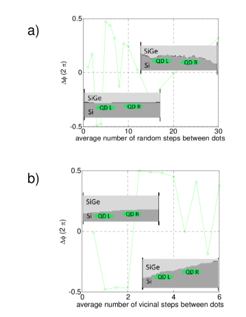
Figure 1 shows the results for simulated SiGe interfaces (horizontal sections separated by vertical steps) for both random (approximately equal numbers of upgoing and downgoing steps) and for vicinal (all steps are upgoing) interfaces. The interfaces were generated by assigning steps at random lateral positions so as to get a particular average lateral density, as indicated in the graphs. As shown, for any roughness, is of large magnitude compared to , and has no systematic dependence on tilt or randomness; these facts both occur because, as discussed above, is large for a single terrace step.
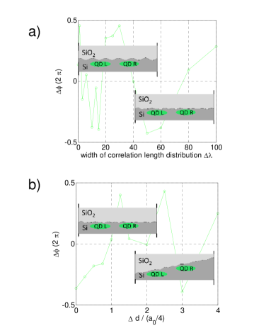
Similar to Figure 1, Figure 2 shows the calculation for appropriate for a Si/SiO2 interface without and with vicinal tilt. We generated this interface by i) first generating a random Fourier transform of variable width , ii) inverse Fourier transforming, and then iii) scaling to give a total vertical height of about 1.5 nm (equivalent to the height of 10 random steps in Figure 1a). In Figure 2a), zero width corresponds to a single correlation length of 20 nm (sinusoidal roughness), and the largest width corresponds to a range of correlation lengths between two and 20 nm. Previous high resolution TEM and weak localization studies of the Si/SiO2 interface have yielded a range of correlation lengths from a few nmIkarashi and Watanabe (2000) up to 100 nmKrivanek and Mazur (1980)Anderson et al. (1993). We see that, as for the SiGe interface, vicinal and non-vicinal randomness with a variety of correlation lengths all lead to large values of .
We now turn to considering an experimental control of and , using gate voltages. Since the valley phase in Equation 6 arises from the vertical height of the interface, at first glance one might think that moving the dot vertically into the Si substrate might have a strong effect on ; although a vertical electric field has strong effect on the magnitude of the coupling[9]-[21], it has a small effect on Saraiva et al. (2009), at least for a flat interface. However, due to the strong dependence of the valley phase on the exact local realization of the interface roughness, using a gate voltage to shift the dot laterally can have a large effect.
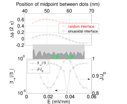
Overall, Figure 3 shows this possibility: the upper panel shows the effect on of using a lateral gate voltage to move both dots laterally with a constant separation, for both a sinusoidal interface () and random interface (). Clearly, the phase difference and the concomitant energies are strong functions of the lateral position; this is simply because moving a dot changes the local interface height, and thus the phase factor in Equation 6. The lower panel shows the concomitant effect on the tunneling matrix elements and on the exchange energy. While the specific gate voltage dependence is likely impossible to predict in advance, this Figure shows that there is the hope of operationally controlling qubit gate frequencies; this experimental control does not depend on our simple analytical frameworkyuan Shiau et al. (2007)Gamble et al. (2013). In comparing Figure 3 to Figures 1 and 2, we note that the systematic appearance of Figure 3 relies on the fact that the interface in that Figure has a correlation length approximately equal to the total range of 20 nm, so that the random structure in apparent in Figures 1 and 2 only appears over the total range of separation in Figure 3.
How can we test the complex valley phase experimentally? First of all, it appears that the global phase (i.e., ) is not measurable, because there is no physical realizable corresponding to it. We suggest two possible experiments for testing directly: i) Measurements of the exchange energy splitting (references Weber et al. (2014)Petta et al. (2005)) in a DQD could be done as a function of multiple lateral gate voltages in the same way as described above. If changes in a systematic way with the lateral position of both dots, this would indicate the likelihood of valley phase-mediated modulation of ; ii) Very recently, valley blockade in a double quantum dot (DQD), exactly analogous to Pauli spin blockadeLai et al. (2011)Shaji et al. (2008)Weber et al. (2014)), has been reportedPerron et al. (2016). In this work, an asymmetry in the size of the bias triangles in a DQD is attributed to blockade in one bias direction due to the impossibility of inter-valley tunneling. Such valley blockade depends on , and thus the leakage current in the blockaded region . Thus, we suggest examining the leakage current magnitude as a function of lateral gate voltage.
Also, we estimate as insignificant the magnitude of spin dephasing (through the dependence of on ) due to charge noise which would modulate the lateral position of one or both dots: From Figure 3, (10 nm), lateral motion (1 nm/10 mV), and a voltage noise magnitude V, we obtain the noise magnitude . Finally, one way of suppressing the complex valley phase effects and of increasing the valley splitting magnitude, would be to make devices with perfectly flat atomically sharp terraces as large as mLi et al. (2011)Tanaka et al. (1996). However, it is likely that subsequent growth of SiO2 or SiGe will lead to substantial roughening of such terraces, and thus it appears likely that these valley phase effects will still be present in typical quantum coherent devices.
It is a pleasure to acknowledge useful discussions with Josh Pomeroy, Mark Stiles, Michael Stewart Jr (all of NIST), Andras Palyi (BUTE), John Gamble (Sandia) and Chris Richardson (LPS).
References
- Zwanenburg et al. (2013) F. A. Zwanenburg et al., Rev. Mod. Phys. 85, 961 (2013).
- Morton et al. (2011) J. J. L. Morton, D. R. McCamey, M. A. Eriksson, and S. A. Lyon, Nature 479, 345 (2011).
- Scarlino et al. (2015) P. Scarlino et al., Phys. Rev. Lett. 115, 106802 (2015).
- Kawakami et al. (2014) E. Kawakami et al., Nature Nanotech. 9, 666 (2014).
- Veldhorst et al. (2014) M. Veldhorst et al., Nature Nanotech. 9, 981 (2014).
- Veldhorst et al. (2015) M. Veldhorst et al., Nature 526, 410 (2015).
- Yang et al. (2013) C. H. Yang et al., Nature Comm. 4, 2069 (2013).
- Hao et al. (2014) X. Hao et al., Nature Comm. 5, 3860 (2014).
- Goswami et al. (2007) S. Goswami, K. A. Slinker, M. Friesen, L. M. McGuire, J. L. Truitt, C. Tahan, L. J. Klein, J. O. Chu, P. M. Mooney, V. W. van der Weide, et al., Nature Physics 3, 41 (2007).
- Shi et al. (2011) Z. Shi et al., Appl. Phys. Lett. 99, 233108 (2011).
- Boykin et al. (2004a) T. B. Boykin, G. Klimeck, M. A. Eriksson, M. Friesen, S. N. Coppersmith, P. von Allmen, F. Oyafuso, and S. Lee, Applied Physics Letters 84, 115 (2004a), URL http://scitation.aip.org/content/aip/journal/apl/84/1/10.1063/1.1637718;jsessionid=eQPbre3FvIyOPAdejAVTNIWa.x-aip-live-03.
- Boykin et al. (2004b) T. B. Boykin, G. Klimeck, M. Friesen, S. N. Coppersmith, P. von Allmen, F. Oyafuso, and S. Lee, Phys. Rev. B 70, 165325 (2004b), URL http://link.aps.org/doi/10.1103/PhysRevB.70.165325.
- Boykin et al. (2008) T. B. Boykin, N. Kharche, and G. Klimeck, Phys. Rev. B 77, 245320 (2008), URL http://link.aps.org/doi/10.1103/PhysRevB.77.245320.
- Friesen and Coppersmith (2010) M. Friesen and S. N. Coppersmith, Phys. Rev. B 81, 115324 (2010), URL http://link.aps.org/doi/10.1103/PhysRevB.81.115324.
- Saraiva et al. (2009) A. L. Saraiva, M. J. Calderón, X. Hu, S. Das Sarma, and B. Koiller, Phys. Rev. B 80, 081305 (2009), URL http://link.aps.org/doi/10.1103/PhysRevB.80.081305.
- Saraiva et al. (2011) A. L. Saraiva, M. J. Calderón, R. B. Capaz, X. Hu, S. Das Sarma, and B. Koiller, Phys. Rev. B 84, 155320 (2011), URL http://link.aps.org/doi/10.1103/PhysRevB.84.155320.
- Srinivasan et al. (2008) S. Srinivasan, G. Klimeck, and L. P. Rokhinson, Applied Physics Letters 93, 112102 (2008), URL http://scitation.aip.org/content/aip/journal/apl/93/11/10.1063/1.2981577;jsessionid=eQPbre3FvIyOPAdejAVTNIWa.x-aip-live-03.
- Gamble et al. (2013) J. K. Gamble, M. A. Eriksson, S. N. Coppersmith, and M. Friesen, Phys. Rev. B 88, 035310 (2013), URL http://link.aps.org/doi/10.1103/PhysRevB.88.035310.
- Culcer et al. (2010a) D. Culcer et al., Phys. Rev. B 82, 205315 (2010a).
- Friesen et al. (2007) M. Friesen, S. Chutia, C. Tahan, and S. N. Coppersmith, Phys. Rev. B 75, 115318 (2007), URL http://link.aps.org/doi/10.1103/PhysRevB.75.115318.
- Friesen et al. (2006) M. Friesen, M. A. Eriksson, and S. N. Coppersmith, Applied Physics Letters 89, 202106 (2006), URL http://scitation.aip.org/content/aip/journal/apl/89/20/10.1063/1.2387975;jsessionid=e8uHB9fAyj0HD4RgKZM7PzA+.x-aip-live-03.
- Wu and Culcer (2012) Y. Wu and D. Culcer, Phys. Rev. B 86, 035321 (2012), URL http://link.aps.org/doi/10.1103/PhysRevB.86.035321.
- Culcer et al. (2010b) D. Culcer et al., Phys. Rev. B 82, 155312 (2010b).
- Huang et al. (2017) W. Huang, M. Veldhorst, N. M. Zimmerman, A. S. Dzurak, and D. Culcer, Phys. Rev. B 95, 075403 (2017).
- Boross et al. (2016) P. Boross, G. Sz chenyi, D. Culcer, and A. P lyi, Phys. Rev. B 94, 035438 (2016).
- yuan Shiau et al. (2007) S. yuan Shiau, S. Chutia, and R. Joynt, Phys. Rev. B 75, 195345 (2007).
- Rahman et al. (2012) R. Rahman, E. Nielsen, R. P. Muller, and M. S. Carroll, Phys. Rev. B 85, 125423 (2012), voltage controlled exchange energies of a two-electron silicon double quantum dot with and without charge defects in the dielectric.
- Ikarashi and Watanabe (2000) N. Ikarashi and K. Watanabe, Jpn. J. Appl. Phys. 39, 1278 (2000).
- Krivanek and Mazur (1980) O. L. Krivanek and J. H. Mazur, Appl. Phys. Lett. 37, 392 (1980).
- Anderson et al. (1993) W. R. Anderson et al., Micro. Eng. 22, 43 (1993).
- Weber et al. (2014) B. Weber et al., Nature Nano. 9, 430 (2014).
- Petta et al. (2005) J. R. Petta et al., Science 309, 2180 (2005).
- Lai et al. (2011) N. S. Lai et al., Sci. Rep. 1, 110 (2011).
- Shaji et al. (2008) N. Shaji et al., Nature Physics 4, 540 (2008).
- Perron et al. (2016) J. K. Perron et al. (2016), unpublished.
- Li et al. (2011) K. Li et al., J. Vac. Sci. Technol. B 29, 041806 (2011).
- Tanaka et al. (1996) S. Tanaka et al., Appl. Phys. Lett. 69, 1235 (1996).
- Streetman (1995) B. G. Streetman, Solid State Electronic Devices (Prentice Hall, Englewood Cliffs, NJ, USA, 1995).
Supplementary Information on Whether the Electron Wavefunction Follows the Interface
In this Section, we will discuss this question as follows:
-
1.
We will give a formal analysis, based on symmetry arguments, that yields the result that the wavefunction follows the interface for any interface slope less than one. This analysis is relevant for the smooth (Si/SiO2) interfaces considered in this paper.
-
2.
We will give an estimate based on energy considerations, that yields the result that the wavefunction follows the interface for any interface roughness with correlation length greater than about 0.3 nm. This analysis is relevant for both step (Si/SiGe) and smooth (Si/SiO2) interfaces considered in this paper.
-
3.
Based on the two analyses, we will present a result from our simulations where we compare the valley phase for i) an interface with vertical steps to ii) an interface with sloped steps, and show that the valley phase is approximately the same for both interfaces. This result shows that the formal analysis (item 1. above) is thus also relevant for the step (Si/SiGe interfaces).
.1 Symmetry Arguments
The Schrodinger equation in the absence of interface roughness is
| (9) |
where is the total electron wavefunction (represented as ) in Equation 3 in the main text. The solution to this equation is , the solution for a flat interface.
We wish to examine the effect on when the interface becomes rough, and in particular on the amount by which the spatial derivatives change. We can define new coordinates
| (10) |
The differentials transform as
| (11) |
The second differentials become
| (12) |
Thus, the second derivatives in the original coordinate system are approximately the same as those in the new system, if . In this case, we can immediately see that . In summary, if the slope of any interface roughness is substantially less than one, the electron wavefunction will approximately follow the interface.
.2 Energy Considerations
Here, we consider the interplay between kinetic and potential energies. For a rough interface, since the accumulation gate produces a potential well in the z-direction at the interface and follows conformally the interface roughness, the electron potential energy will be lowered if the wavefunction follows the interface roughness exactly (Fig. S2). On the other hand, the more the wavefunction follows the interface roughness, the larger is the kinetic energy increase. For simplicity, we consider only one lateral direction .
Thus, we determine the approximate maximum bending of the electron wavefunction by the constraint
| (13) |
in the effective mass approximation (EMA). Note that, for this inequality, the normalization of the wavefunction is present on both sides, so we will suppress the normalization factor.
We define the following parameters:
-
Electron envelope wavefunction in the EMA.
- (x)
-
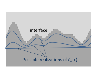
Height of center of electron wavefunction (as distinguished from the height of the interface ). [See Figure 4]
-
Amplitude of local bending of electron wavefunction (assumed to be quadratic).
-
Correlation length of electron wavefunction (as distinguished from the correlation length of the interface).
-
Band offset between Si and SiO2, as in Equation 5 of the main text.
-
Vertical thickness of electron 2DEG (inversion layer thickness).
-
Effective mass of transverse electron in Si; .
.2.1 Kinetic Energy
To approximate the left-hand side of Equation 13, we start by assuming that the wavefunction is locally quadratic:
| (14) |
Following Equation 3 in the main text, the EMA envelope wavefunction is
| (15) |
A good approximation to the z-dependence of the 2DEG is (ref Streetman (1995)). The contribution to the kinetic energy from the roughness of the 2DEG comes only from this part of the total wavefunction (x, z):
| (16) |
With the quadratic dependence of (x), and evaluating at , we obtain
| (17) |
With 5 nm / 0.5 nm,
| (18) |
Finally, the left hand side of Equation 13 is
| (19) |
.2.2 Potential Energy
We approximate the vertical potential well at the interface as triangular, with the sloped section having a slope of . The decrease in potential energy when the electron wavefunction is bent with a vertical change of approximately instead of flat is thus
| (20) |
.2.3 Summary
Combining Equations 13, 19, 20, we thus obtain a constraint on the minimum radius of curvature or correlation length of the electron wavefunction
| (21) |
using the values in this section ( 3 eV for Si/SiO2), we finally obtain 0.3 nm. Given that the typical amplitude of roughness is less than or of order 1 nm, this condition is quite similar to that in the previous argument based on symmetry considerations.
.3 Results from Simulations
Figure 5 shows two choices for (x), with the smoothed one obeying the approximate constraints derived in the last two sections. We simulated the phase difference, and got the result
| (22) |
Thus, the results of a combination of i) two theoretical constraints on the sharpness of the electron wavefunction as viewed through (x), and ii) the very small phase difference for the sharp versus smoothed electron wavefunctions, demonstrate that our assumption in the main text (that the electron wavefunction follows the interface roughness) does not present a significant offset in our results.
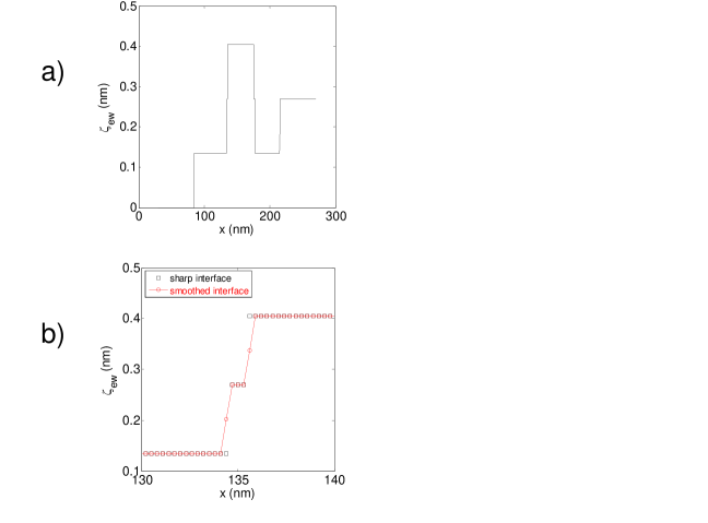
.4 Using only the Ground Orbital State
In this section, we give the assumption underlying the use of only the ground orbital state, and discuss the plausibility of this assumption.
For a flat interface, we can identify the eigenstates as , following Equation 3 in the main text. Here, is the orbital state index, and , are the two possible valley states.
For the full treatment of the rough interface, we would consider a potential , where is the potential in Equation 5 in the main text, and is a perturbation on the flat interface potential. In this case, in order to calculate the full eigenstates, we would consider Hamiltonian matrix elements , including intra-valley intra-orbital, intervalley intra-orbital, and intervalley inter-orbital terms. The first two types of terms, while leading to mixing of the orbital states, will not affect our results for the valley phase.
However, the last term (intervalley and inter-orbital) will affect, and in particular will likely make substantially smaller through statistical averaging, the valley phase. The relevant parameter that determines the level of intervalley interorbital mixing is .
Thus, the assumption underlying the use of only the ground orbital states is that . There are two arguments for believing that this approximation is justified:
-
1.
Theoretical estimate: The numerator of is apparently less than the valley splitting , where is the ground orbital state. Since the valley splitting gets smaller as the interface roughness increases, while the orbital energy splitting stays the same, it appears that will be substantially less than one for a rough interface.
- 2.
.5 Files
All pathnames are relative to L:/internal/SET_team/Neil/other peoples documents/Culcer/valleys 14_5
- Text:
-
/manuscript/text/Culcer_valley_phase_v_2.tex.
- All figures
-
/manuscript/figures/15_11 portrait Culcer phase figures.pptx.
- Fig 1
-
Main: /manuscript/figures/Delta phi plots/Step_NonVicinal.dat and Step_Vicinal.dat using do_plot_step_vicinal.m.
- Fig 2
-
Main: /manuscript/figures/Delta phi plots/Sin_NonVicinal.dat and Sin_Vicinal.dat using do_plot_sin_vicinal.m.
- Fig 3 both panels
-
manuscript/figures/voltage control/VoltageControl_XL10.dat and _XL0.dat using do_plot_voltage_control.m.
- Fig S1
-
/manuscript/figures/15_11 portrait Culcer phase figures.pptx.
- Fig S2
-
/manuscript/figures/smoothed for Supp/xi_x_steps_tilt_0_rand_1.dat, using do_plot_smoothed_unsmoothed.m, followed by xli, cla, plot(x, y, ’k-’)