FemtoDAQ: A Low-Cost Digitizer for SiPM-Based
Detector Studies
and its Application
to the HAWC Detector Upgrade
Abstract
The FemtoDAQ is a low-cost two channel data acquisition system which we have used to investigate the signal characteristics of silicon photomultipliers (SiPMs) coupled to fast scintilators. The FemtoDAQ system can also be used to instrument low cost moderate performance passive detectors, and is suitable for use in harsh environments (e.g., high altitude). The FemtoDAQ is being used as a SiPM test bench for the High Altitude Water Cherenkov (HAWC) Observatory, a TeV gamma ray detector located 4100 m above sea level. Planned upgrades to the HAWC array can benefit greatly from SiPMs, a robust, low-voltage, low-cost alternative to traditional vacuum photomultipliers. The FemtoDAQ is used to power the SiPM detector front end, bias the SiPM, and digitize the photosensor output in a single compact unit.
I Introduction
The capture, digitization, and postprocessing of waveforms from photosensors is among the most common measurements performed in nuclear and high-energy physics. Traditionally such measurements require a significant investment in space and equipment, with researchers custom designing test benches out of components found in the laboratory: benchtop or rack-mounted power supplies, amplifiers, digitizers, readout hardware and software, etc. While this kind of equipment is accessible to scientists and engineers in most professional settings, its cost (and the expertise needed to run it) is often beyond the capabilities of students and educators.
However, the continuing drop in the cost of computers and electronics now makes it possible to design powerful and compact data acquisition systems using commercial off-the-shelf components. In this paper we describe such a system, called the FemtoDAQ [1].
The FemtoDAQ is a two-channel data acquisition computer with signal processing capabilities. It is designed to power and read out silicon photomultipliers (SiPMs) but can interface with traditional photomultipliers (PMTs) and be used in a wide variety of experiments. Its compact size makes it easy to transport and well-suited for remote applications. In addition, a simple Python-based programming layer makes the unit easy to use in the classroom, but it is powerful enough to act as a drop-in replacement for a full-fledged laboratory test bench. We are currently using the FemtoDAQ to characterize silicon photomultipliers (SiPMs) for the High-Altitude Water Cherenkov (HAWC) Observatory, a US-Mexican facility built to observe astrophysical gamma rays [2].
This paper is organized as follows. In Section II we describe the components of the FemtoDAQ, the basics of its operation, and a simple example of its capabilities. In Section III we describe the HAWC detector and a study of SiPMs for use in HAWC. We summarize the status of our current work and discuss future directions and applications in Section IV.
II Description of the FemtoDAQ LV-2
The FemtoDAQ, shown in Fig. 1, is a commercial single-board BeagleBone Black computer [3] with two custom-designed mezzanine boards. The first mezzanine board is specifically designed to interface with silicon photomultipliers. SiPMs are being rapidly adopted in fields such as medical imaging, astronomy, and high-energy physics due to their low cost, low power and voltage requirements, high gain, and relative durability compared to PMTs.
The power board in the FemtoDAQ provides 10 V to 90 V DC bias voltage to the front-end electronics required to operate two SiPMs. This range makes the board compatible with commercially available SiPMs from manufacturers such as Hamamatsu [4] and SensL [5]. A ribbon cable connector is available for interfacing with external devices over SPI and I2C busses. The busses enable reading of remote temperature sensors to compensate the SiPM bias for temperature fluctuations and maintain a constant gain.
The second mezzanine board digitizes two analog inputs with 14-bit ADCs digitizing at 100 MSPS. An antialiasing Bessel filter is applied to the waveforms to suppress high-frequency noise and stretch very fast signals. An onboard field programmable gate array (FPGA) then performs pulse detection and extracts pulse characteristics using digital signal processing. The input section has a V range with selectable input impedance: 50 , 1 k, and 100 k. Four logic input/output signals (3.3 V CMOS) are provided for external triggering or external veto.
While the FemtoDAQ power/bias board has been designed with the testing of SiPMs in mind, the input board is agnostic to the type of input sensor. The only limitations are the input impedance levels and signal range. Hence, it can be used to test SiPMs and similar detectors such as PIN diodes and multi-pixel photon counters, as well as PMTs (with an appropriate external HV supply). The FemtoDAQ has been extensively tested with both SiPMs and PMTs.
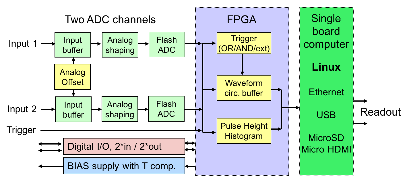
II-A Triggering, Data Capture, and Recording
The flow and control of data in the FemtoDAQ is shown in Fig. 2. After digitization, a trigger condition is applied by the onboard FPGA. The trigger thresholds are specified by the user and can be defined independently for the two input channels or as a coincidence trigger on both channels. One of the logic inputs also provides an optional external trigger.
Captured waveforms are stored in a circular buffer with a storage length of 81.92 s per waveform per channel. Users can read out individual triggered waveforms or instruct the FPGA to compute a pulse height histogram for all triggers captured on each channel within a user-defined time period. Histograms are stored with 12-bit resolution (4096 bins per channel). For histogramming in situ, the pulse height is analyzed by a rolling average with a selectable bin size. Other DSP filters, such as baseline subtraction, differentiation, etc. are also implemented in the FPGA.
The FemtoDAQ contains onboard flash storage with 4 GB capacity, shared with the Linux OS installed on the BeagleBone Black computer. The use of solid-state memory allows the device to be used in a variety of harsh environmental conditions, including very high altitudes.
Users interact with the FemtoDAQ via the BeagleBone, which is powered by a 1 GHz ARM processor with floating point hardware and ships with Debian Linux running on board. The FemtoDAQ can be run as a standalone computer; an HDMI connector is provided for connections to a local monitor, and a mouse and keyboard can be connected via a USB type A connector. A MicroSD socket is available for storing acquired waveforms, histograms, and event files. In addition, the network interface provided with the BeagleBone allows output to be written to NFS-mounted remote disks.
Alternatively, the FemtoDAQ can be mounted as a peripheral device on a host computer using available Ethernet or USB-2 connectors on the main board. Free device drivers available from BeagleBone are used to mount the FemtoDAQ on hosts running Windows, Linux, and Mac OS X; extensive tests have been performed using Windows 8 and 10, Ubuntu 15.10, and Mac OS 10.11.
II-B Programming and User Interface
The FemtoDAQ presents the user with several programming interfaces which can be customized for different applications. At the lowest level, users can control hardware settings in the FPGA and input channels using commands sent to the unit. These commands are used to adjust triggering and processing of waveforms such as trigger levels, baseline subtraction, boxcar averaging, coincidence conditions, etc. If the FemtoDAQ is powering one or two SiPMs, the command interface can also be used to remotely adjust the bias voltage supplied by the power board.
A Python module is provided to parse terminal input from the user and pass commands to the onboard FPGA. The module is open-source and can be customized or altered by the end user. This interface allows for a wide variety of scripting and automation: for example, automatic timed measurements with adjustments of bias voltage during the course of data taking.


While the FemtoDAQ is relatively easy to control via the command line, an intuitive high-level graphical user interface (GUI) based on the wxPython library is also provided. The GUI, shown in Fig. 3, allows users to change the SiPM bias, enable internal test pulses, adjust baseline correction and boxcar averaging, enable coincident triggers, and switch between waveform capture mode and pulse height histogram mode. Online plotting capabilities are also provided so that users can immediately view waveforms and histograms (Fig. 4).
For offline analysis, waveforms can be saved in one of several binary and text formats – e.g., comma-separated variable tables of ADC count versus clock – and analyzed on the BeagleBone or saved to network disks or host computers.
II-C Example Application: Energy Resolution of LYSO
To demonstrate the capabilities of the FemtoDAQ we provide data from two simple studies: a nuclear/particle counting application in which a SiPM is coupled to a LYSO scintillator, and a timing test of two SiPMs read out simultaneously in both channels.
LYSO is a high-density scintillator commonly used in PET due to its high efficiency for 511 keV photo-peak detection [6]. It is also of interest for National Security applications because of its high efficiency and good timing properties [7]. A challenge is its internal radioactivity caused by traces of 176Lu.
Energy histograms from a 1 cm3 LYSO scintillator are plotted in Fig. 5. The scintillator was optically coupled to a single 6x6 mm Series-C SiPM manufactured by SensL [9], and the output from the SiPM was amplified by a factor of using a custom-made carrier board. A 22Na source was placed on top of the crystal, and the resulting light signals observed by the SiPMs were used to self-trigger the FemtoDAQ and produce a pulse height histogram. A “free run” pulse height histogram due to the intrinsic 176Lu activity was then subtracted from the measurement of the 22Na source with the same crystal. Both histograms were produced using the in situ histogrammming capabilities of the firmware.
The 511 keV peak observed in the scintillator was fit offline using a Gaussian and determined to be 74.8 keV FWHM, or about 14.6%. This peak resolution is typical for LYSO [8].


II-D Example Application: SiPM Timing
The second demonstration of the capabilities of the FemtoDAQ is a measurement of the relative timing of two SiPMs observing a common light source.
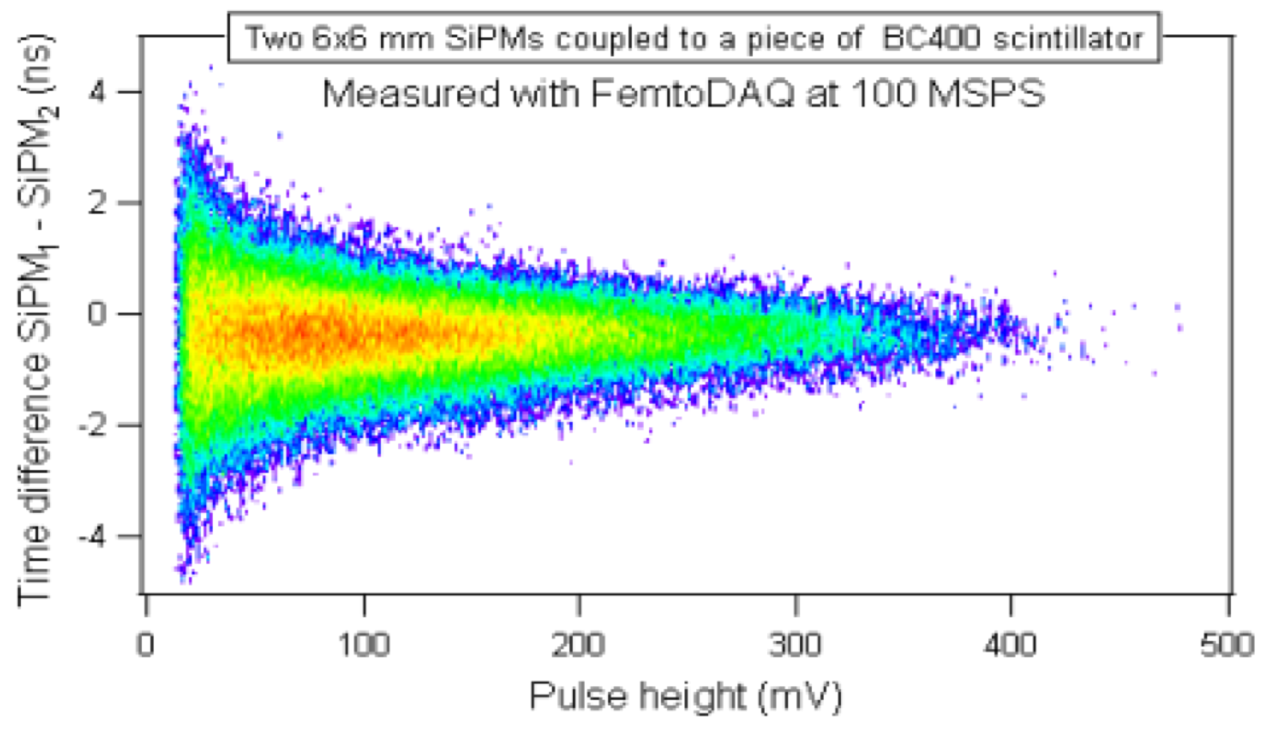
We measured the timing using digitized signals from two 66 mm SiPMs coupled to a single piece of BC400 irradiated with particles from a thick natural 232Th source. The 10 amplified signals were digitized with two FemtoDAQ channels in self-triggered mode. A total of events were recorded, each consisting of two correlated waveforms from both SiPMs. The event file was processed offline.
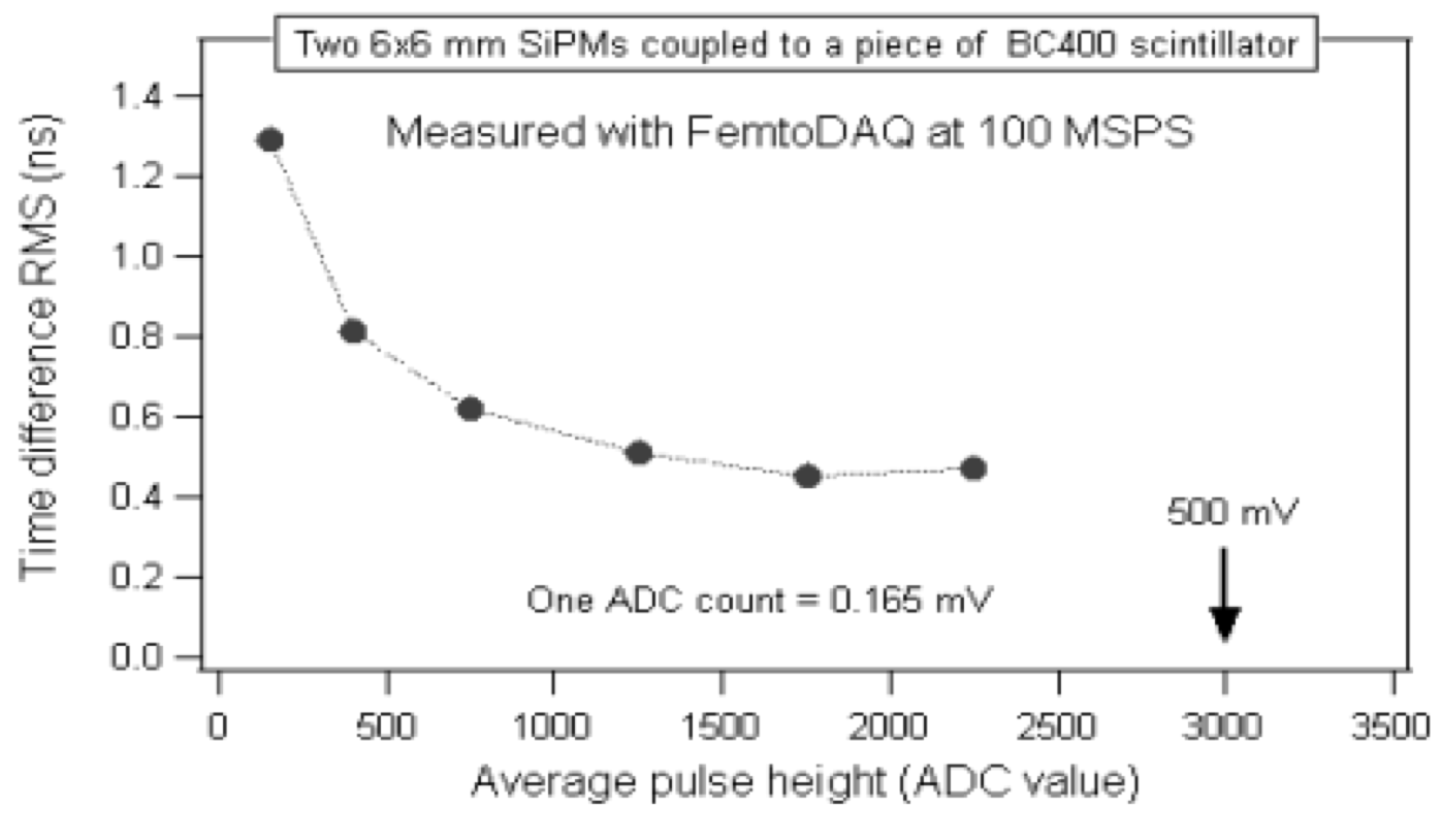
In Fig. 6 we show the time difference between SiPM1 and SiPM2 plotted versus the average pulse height . The lower part of the figure shows the RMS projections of the 2-dimensional distribution as a function of average pulse height. The largest pulse height corresponds to particles of about 6 MeV (in air) from 212Po decay in the source.
We observed an improvement in the relative timing as a function of pulse height; the highest amplitude events achieved 450 ps RMS, which is 4.5% of the sampling clock. The largest pulses correspond to about 15% of the full 14-bit ADC range of 16 384 ADC counts.
III The HAWC Gamma-Ray Observatory
The HAWC Observatory is designed to observe the extensive air showers produced when astrophysical rays and cosmic rays interact in the atmosphere and produce a high-energy particle cascade. HAWC is a collaboration of 30 academic institutions and national labs in the US, Mexico, and Europe. The detector is located 4100 m above sea level in Sierra Negra, Mexico, and is optimized to detect rays and cosmic rays between 100 GeV and 100 TeV.
The detector is a 20 000 m2 array of 300 close-packed water Cherenkov detectors (WCDs). Each WCD contains 200 kL of purified water. When relativistic charged particles from extensive air showers pass through the water they produce ultraviolet Cherenkov light. Three 8” hemispherical PMTs and one 10” PMT located at the bottom of each tank (for a total of 1200 PMTs in the full array) are used to detect the Cherenkov photons. By combining the timing information and spatial distribution of PMTs triggered by an air shower, the arrival direction, energy, and type of the primary particle can be identified. In this manner, air showers produced by cosmic rays can be filtered out of the data during offline processing, and the remaining rays are used to produce sky maps of -ray sources.
III-A High-Energy Upgrade
The construction of HAWC was completed in December 2014, and a high-energy upgrade to the detector is now underway. To increase the sensitivity of the observatory above 10 TeV, the collaboration will deploy 350 “outrigger” tanks in a sparse array surrounding the 300 WCDs already at the site [11].
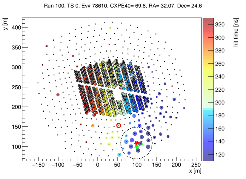
The purpose of the outriggers is to help localize high-energy air showers that impact just outside the central array. Currently these air showers are poorly reconstructed and must be removed from the analysis of cosmic-ray and -ray events. However, with the outrigger tanks in place, the “uncontained” showers currently lost to quality cuts can be recovered. An example of such an event is shown in Fig. 7.
The design of the outrigger stations and readout electronics is in progress and deployment of the outrigger stations will begin in late 2016. The outrigger upgrade is expected to increase the effective area of HAWC by a factor of four above TeV.
III-B Testing SiPM Detectors for Use in HAWC
The baseline design of an outrigger station calls for the use of an 8” Hamamatsu R5912 hemispherical PMT, but the upgrade presents an excellent opportunity to field-test new photosensor technologies such as SiPMs. SiPMs have many advantages over PMTs as described in Section II, and are the focus of considerable manufacturer R&D. The technology is experiencing significant year-over-year improvements in quality and performance, and is an excellent candidate to replace PMTs in water Cherenkov experiments in the near future.
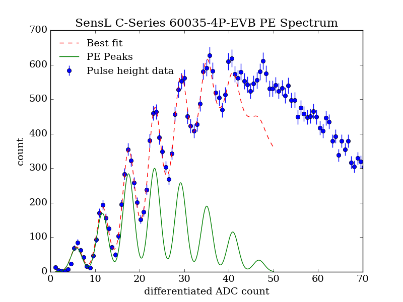
We have used the FemtoDAQ in the laboratory to characterize the basic properties of SiPMs that are important for a photon counting experiment such as HAWC – for example, single photoelectron (PE) response, dark count rate, gain, etc. For this study we have focused on the SensL C-Series 60035-4P-EVB, a array of 3 mm silicon photosensors. The photon detection efficiency of the sensor peaks at 40% between 400 and 450 nm, and its gain ranges from to as the overvoltage is increased from 1 V to 5 V.

Our setup for testing the photon-counting response of the SiPM array is shown in Fig. 8. The array is seated on a custom carrier board which provides amplification. The board acts as a front end to the FemtoDAQ, which provides a bias voltage via its internal power board.
The SiPM has been placed inside a dark box with a 5 mm UV (400 nm) LED. A Quantum Composer 9520 pulse generator is used to pulse the LED with extremely narrow ( ns) square pulses, so that on average only a few photons are emitted per pulse. The generator output is split between the LED and Channel 1 of the FemtoDAQ, with the output from the SiPM sent to Channel 2.
To observe the single PE response of the SiPM, the FemtoDAQ has been set up to trigger on coincident input from the split pulser signal (Channel 1) and the SiPM (Channel 2). By gating the SiPM output in this manner we can effectively eliminate dark counts from the triggered output. (Note that in the current generation of SiPMs, the dark count rate can be considerable depending on the overvoltage and temperature of the sensor. At 20 C, the dark count rate from the C-Series array is typically of order 1 MHz.)
The SiPM output has a very long RC tail (s) because each cell in the device is connected in series to a quenching resistor [10]. The tail can cause a pile-up effect when the photon rate (or dark count rate) is too high, so we have chosen to remove it by numerically differentiating the digitized output from Channel 2 of the FemtoDAQ. This is roughly analogous to shaping the signal with a CR-RC circuit in a NIM crate.
After differentiation, the SiPM waveform is transformed from a set of rising edges with exponential tails to a set of well-isolated peaks. The peaks have a small undershoot which we compensate with offline processing (though this could also be done internally by the FPGA). The pulse height histogram of the processed waveform is plotted in Fig. 9. Individual Gaussian peaks from single and multiple PE events are clearly visible, while the dark counts are strongly suppressed by the coincidence trigger. From the pulse height histogram, we can easily set up calculations of the dark count rate and relative gain as a function of bias voltage.
IV Conclusion
The FemtoDAQ is a compact two-channel digitizer and signal processing unit designed to read out a wide variety of commercial photosensors. Though it is built atop the BeagleBone Black single-board computer, which is designed for hobbyists, it is powerful enough to be employed in a laboratory setting. In addition, its network capability and Python-based user interface allow for many kinds of automated and/or remote measurements. We are currently using it to characterize the performance of SiPMs for the outrigger upgrade of the HAWC Observatory.
The FemtoDAQ is also simple and robust enough for classroom use, and can be operated easily by undergraduates and high school students. Educators with a passing knowledge of Python can use the FemtoDAQ to design and carry out a large number of classic university-level nuclear and particle physics experiments, two of which were demonstrated in this paper. The compactness of the device also suggests many interesting outreach activities, and we are working with local educators to design outreach programs.
Acknowledgment
WS acknowledges support in this work by the Department of Energy Office of Science, Office of Nuclear Physics under grant numbers DE-SC0009543 and DE-SC0013144. SB is supported by the Office of High Energy Physics under grant number DE-SC0008475. We are indebted to Mr. David Hunter for implementing the graphical user interface.
References
- [1] FemtoDAQ: http://www.FemtoDAQ.com
- [2] HAWC Collaboration: A. U. Abeysekara et al., “Sensitivity of the High Altitude Water Cherenkov Detector to Sources of Multi-TeV Gamma Rays,” Astropart. Phys., vol. 50-52, pp. 26-32, 2013.
- [3] BeagleBone Black: http://beagleboard.org/black
- [4] Hamamatsu Datasheet: “MPPC and MPPC module for precision measurement,” Hamamatsu Photonics K. K., Solid State Division, March 2016.
- [5] SensL Technologies Ltd., http://sensl.com, 2016.
- [6] J. Du, Y. Wang, L. Zhang, Z. Xu, and X. Wang, “Physical Properties of LYSO Scintillator for NN-PET Detectors,” BMEI, vol. 1, pp. 314-318, Oct. 2009.
- [7] H. M. Park, S. J. Jeon, H. K. Lee, K. S. Joo, “Design of a silicon photomultiplier based compact radiation detector for Homeland Security screening,” ANIMMA, pp. 1-5, June 2013.
- [8] T. Kimble, M. Chou, and B.H.T. Chai, “Scintillation properties of LYSO crystals,” in Proc. IEEE Nucl. Sci. Symp. Conf., vol. 3, pp. 1434-1737, 2002.
- [9] SensL Datasheet: “C-Series: Low Noise, Blue Sensitive Silicon Photomultipliers,” SensL Technologies Ltd., 2014.
- [10] SensL Technical Note: “SiPM Experiment Guide,” SensL Technologies Ltd., 2014.
- [11] A. Sandoval (HAWC Collaboration), “HAWC Upgrade with a Sparse Outrigger Array,” in Proc. 34th Int. Cosmic Ray Conf., 2015.