Monitoring Electrostatically-Induced Deflection, Strain and Doping in Suspended Graphene using Raman Spectroscopy
Abstract
Electrostatic gating offers elegant ways to simultaneously strain and dope atomically thin membranes. Here, we report on a detailed in situ Raman scattering study on graphene, suspended over a Si/SiO2 substrate. In such a layered structure, the intensity of the Raman G- and 2D-mode features of graphene are strongly modulated by optical interference effects and allow an accurate determination of the electrostatically-induced membrane deflection, up to irreversible collapse. The membrane deflection is successfully described by an electromechanical model, which we also use to provide useful guidelines for device engineering. In addition, electrostatically-induced tensile strain is determined by examining the softening of the Raman features. Due to a small residual charge inhomogeneity , we find that non-adiabatic anomalous phonon softening is negligible compared to strain-induced phonon softening. These results open perspectives for innovative Raman scattering-based readout schemes in two-dimensional nanoresonators.
Keywords: suspended graphene, two-dimensional materials, Raman spectroscopy, strain, doping, optical interference, NEMS.
Introduction Electrostatic gating is one of the most commonly employed actuation schemes in nanomechanical resonators Ekinci (2005). In particular, field-effect transistor geometries have been adapted to fabricate nano-electromechanical resonators using individual carbon nanotubes Sazonova et al. (2004), graphene Bunch et al. (2007); Chen et al. (2009) and, more recently, atomically thin transition metal dichalcogenides Lee et al. (2013); Castellanos-Gomez et al. (2013). In such devices, the ultimate thinness of the suspended nanoresonator leads to high electromechanical susceptibility and possible coupling between electrostatically-induced strain and doping. As a classic example, similar designs of suspended graphene transistors have been used not only to fabricate electro-mechanical Chen et al. (2009) or opto-electromechanical devices Bunch et al. (2007); Barton et al. (2012); Reserbat-Plantey et al. (2012) but also to probe quasi-ballistic electron transport Bolotin et al. (2008); Du et al. (2008) and many-body effects Elias et al. (2011); Faugeras et al. (2015) in the vicinity of graphene’s charge neutrality (Dirac) point. Electrostatic pressure can thus intentionally be applied to control the position, shape, and motion of an atomically thin suspended membrane but may also be an undesired side-effect when examining intrinsic transport properties Huang et al. (2011); Zhang et al. (2014); Medvedyeva and Blanter (2011), ultimately leading to irreversible collapse Bolotin et al. (2008); Bao et al. (2012). As a result, in situ probes are needed in order to examine the subtle interplay between doping, electron transport, motion and strain in electrostatically-actuated membranes.
Here, we employ micro-Raman scattering spectroscopy as a minimally invasive and highly accurate technique to simultaneously monitor electrostatically-induced deflection, strain and doping in a pristine suspended graphene monolayer. Our analysis is based on the large changes in intensity, frequency, and linewidth of the main Raman features of graphene subjected to an electrostatic pressure. The measured deflection is well-captured by an electromechanical model Landau and Lifshitz (1970); Medvedyeva and Blanter (2011); Bao et al. (2012), which solely uses the built-in tension in graphene as a fitting parameter. Our model accurately predicts the critical gate bias and highest doping level achievable before device collapse, therefore providing useful guidelines for opto-electromechanical device engineering. Here, the charge carrier density remains significantly below , with a small residual charge inhomogeneity of . In these conditions, the Raman features of electrostatically-gated suspended graphene are chiefly affected by strain-induced phonon softening, with only minor contributions from non-adiabatic electron-phonon coupling Lazzeri and Mauri (2006); Ando (2006); Yan et al. (2008).
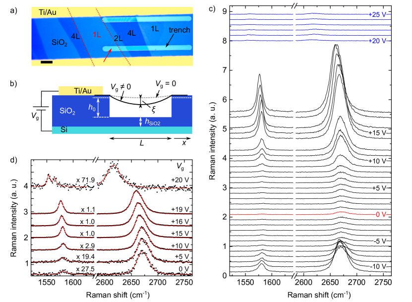
Methods Our typical sample consists of a mechanically exfoliated graphene monolayer suspended over a m-wide trench pre-patterned by optical lithography and reactive ion etching on a Si/SiO2 substrate (oxide thickness of nm, of which nm of SiO2 are left) Berciaud et al. (2009). The suspended monolayers (1LG) are identified via optical microscopy and Raman spectroscopy as discussed below. To avoid contamination with resist and solvents, Ti/Au contacts are evaporated through a transmission electron microscopy grid, used as a shadow mask (see Fig. 1a,b). Finally, the gold contact pads are wire-bonded and the sample is cooled down to K using an He flow optical cryostat. Micro-Raman spectra are recorded as a function of the back-gate voltage in back-scattering geometry using a laser beam with a wavelength of nm focused onto a -diameter spot onto the sample using a objective with a numerical aperture of . The laser power impinging on the sample is maintained below W to avoid photothermally-induced changes in the Raman features and sample damage. In the following, we focus on the Raman G and 2D modes, which involve zone-center and near zone-edge optical phonons, respectively Ferrari and Basko (2013). The defect-allowed D-mode has a negligible intensity and is not considered here. The peak frequency (), full-width at half maximum (), and integrated intensity () of the G-mode and 2D-mode features are extracted from single Lorentzian and modified Lorentzian fits Basko (2008); Berciaud et al. (2013), respectively. As previously demonstrated Bolotin et al. (2008); Du et al. (2008); Elias et al. (2011); Berciaud et al. (2009); Ni et al. (2009); Berciaud et al. (2013); Metten et al. (2013) and also shown in the Supporting Information, suspended graphene exhibits low residual charge carrier density and inhomogeneity, both below cm-2. Consequently, we assume that graphene is quasi neutral at . We note , the initial distance between the membrane and the underlying SiO2 layer at and the gate-induced deflection in the middle of the trench (see Fig. 1b).
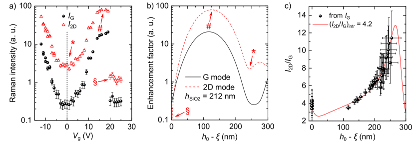
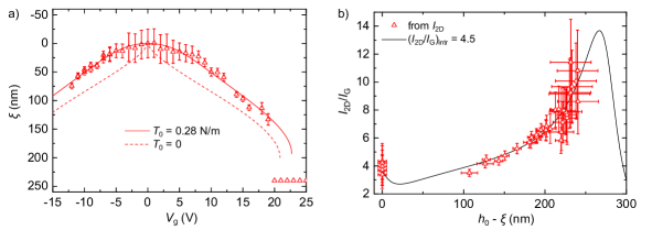
Electrostatically-induced deflection Figure 1c shows a cascade plot of Raman spectra recorded during a gate bias sweep from to . Several interesting features can be observed as rises up to V. First, the integrated intensity of the Raman features increases strikingly. Second, as can be more clearly seen in Fig. 1d, the integrated intensity ratio of the 2D- and G-mode features, , augments significantly. Third, the Raman G- and 2D-mode features downshift. The first and second observations stem from optical interference effects, which have a drastic impact on the Raman intensities in graphene devices within a multilayered structure Yoon et al. (2009); Reserbat-Plantey et al. (2013); Metten et al. (2014). Indeed, the applied gate bias induces an electrostatic pressure that pulls the graphene layer towards the underlying SiO2 layer, leading to gate-dependent Raman enhancement factors. For a quantitative analysis, and are plotted as a function of in Fig. 2a (this plot includes a gate sweep from to V and from to V), along with, in Fig. 2b, the Raman enhancement factors for the G- and 2D-mode features, computed using a multiple interference model Yoon et al. (2009); Metten et al. (2014). From this model, we are able to estimate the central deflection .
Here, and are minimal for and, as expected, show nearly identical behaviors at positive and negative . Interestingly, increases from its minimal value at to a maximum at V, which we assign to an initial height and to a deflection , respectively. We note that is a little smaller than the actual depth of the trench (), implying that the graphene membrane is slightly concave. This situation may be attributed to the mismatch between the thermal expansion coefficients of the Si/SiO2 substrate and of graphene Bao et al. (2009); Yoon et al. (2011), as well as to the native slack of the as-exfoliated sample and adhesion to the sidewalls of the trench Chen et al. (2009); Singh et al. (2010); Bunch et al. (2008); Kitt et al. (2013); Metten et al. (2014). Since the Raman-scattered G- and 2D-mode photons have different wavelengths, the measured ratio , also depends on (see Fig. 2c) Yoon et al. (2009); Metten et al. (2015) and is in very good agreement with the calculated Raman enhancement factors 111In the range of gate biases applied here, and are expected to vary marginally due to electrostatically-induced doping Yan et al. (2007); Froehlicher and Berciaud (2015) using an interference-free intrinsic ratio of , consistent with our previous findings Metten et al. (2015).
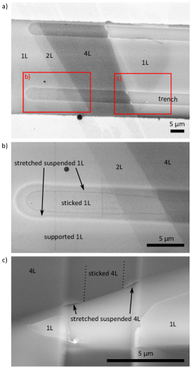
The sudden drop in the Raman intensities above V (see Fig. 1c-d and 2a) is inconsistent with a continuous increase of and is a strong indication that the membrane has collapsed and now adheres strongly to the underlying SiO2 layer. Indeed, the Raman intensity is expected to be very low for the layered system Si/SiO2(212 nm)/graphene/vacuum when (see Fig. 2b). The drop in the Raman intensities is accompanied by a downshift of the G- and 2D-mode features and by a splitting of the G-mode feature, characteristic of sizable uniaxial strain Mohiuddin et al. (2009); Huang et al. (2009) (see Fig. 1d). These observations suggest that the membrane remains attached on the edges of the trench, as confirmed by scanning electron microscopy (SEM) imaging (see Supporting Information). The G- and 2D-mode downshifts allow us to estimate a uniaxial strain of Mohiuddin et al. (2009), that is consistent with a rough estimation based on the SEM image.
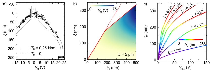
Fig. 3a displays as a function of , extracted from the variations of . Very similar results are obtained from the analysis of (see Supporting Information). The large error bars near account for the broad valley in the interference pattern (see Fig. 2b). From the theory of elasticity Medvedyeva and Blanter (2011); Bao et al. (2012), is connected to a (here electrostatic) pressure load through
| (1) |
where is the Young’s modulus, the Poisson ratio, the thickness of the membrane, its built-in tension, and the trench width (see Fig. 1b). The scaling is well-known for membranes (with no bending rigidity) Hencky (1915); Komaragiri et al. (2005); Yue et al. (2012), and can be interpreted as an effective bending rigidity moderating the deflection, as scales linearly with for thin plates Landau and Lifshitz (1970); Vlassak and Nix (1992); Beams (1995); Williams (1997); Medvedyeva and Blanter (2011). Eq. (1) is obtained by assuming translational invariance along the trench and a parabolic membrane profile perpendicular to the trench ( direction), which is a first approximation, because back-coupling mechanisms between deflection and charge redistribution may affect the membrane profile Medvedyeva and Blanter (2011). Noteworthy, Eq. (1) also involves a uniform pressure load over the membrane, which is not the case in our experiment since attains values that are on the same order of magnitude as . However, we can model our experimental data by considering an effective value of , obtained by averaging the local capacitance along the parabolic profile (see Fig. 1b) Bao et al. (2012):
| (2) |
with , and , where is the distance between the SiO2 layer and the membrane, is the vacuum permittivity and is the DC dielectric constant of SiO2. We can thus compute as a function of by injecting Eq. (2) into Eq. (1) and solving the resulting equation numerically.
As shown in Fig. 3a, our experimental measurements of vs are very well fit to Eq. (1), using TPa, nm and Bacon (1951); Lee et al. (2008); Jiang et al. (2009); Metten et al. (2014) and leaving as the only fitting parameter. This value corresponds to a built-in tension of , which is consistent with previous studies of suspended graphene monolayers Bunch et al. (2007); Chen et al. (2009); Lee et al. (2008); Huang et al. (2011); Metten et al. (2013). Let us note that the good agreement between our data and our model using an intrinsic value of Lee et al. (2008); Bao et al. (2012); Koenig et al. (2011); Metten et al. (2014); Jiang et al. (2009) suggests that crumpling in our mechanically exfoliated graphene membrane can presumably be neglected Nicholl et al. (2015).
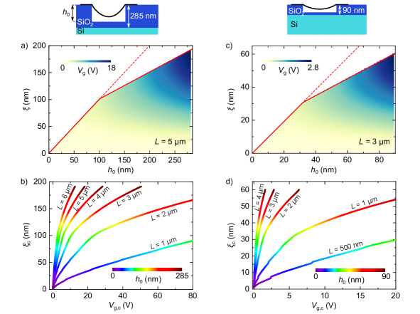
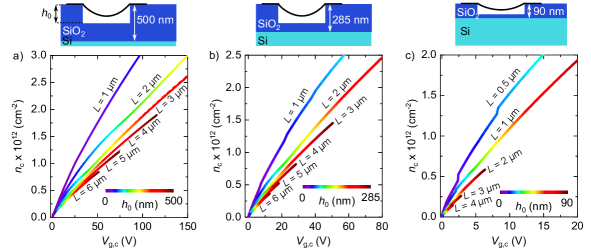
Interestingly, Eq. (1) has no real solution above a critical gate voltage . In particular, our model predicts an abrupt increase of for V up to V, consistent with the collapse of the membrane observed for . We rely on the good accordance of our data with the electromechanical model to calculate the gate-induced deflection for a range of and compute the critical voltage above which no real solution is found. The resulting contour plot is shown in Fig. 3b for and an initial SiO2 thickess of . Interestingly, for , we find that increasing leads to a smooth deposition of the graphene layer onto the underlying SiO2 substrate (i.e., the critical deflection ), whereas for (as is the case in our experiment) the membrane abruptly collapses after reaching a value . Now, another interesting question for device optimization is, which voltage does a membrane sustain (oxide breakdown notwithstanding) until the membrane collapses? In Fig. 3c, the critical lines () are shown for different , with color-coded . In order to estimate the impact of a typical built-in tension, the critical lines for and m are added for N/m. A finite built-in tension slightly shifts the curves to higher and retards the deflection and the collapse. Similar simulations for trenches etched in a Si/SiO2 substrate with initial SiO2 thicknesses of and are reported in the Supporting Information.
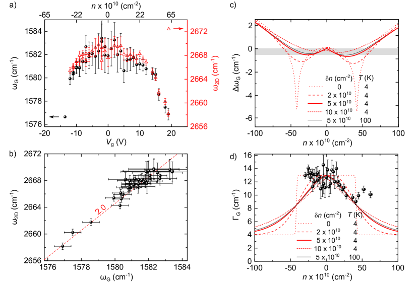
Electrostatically-induced strain and doping The strength of our Raman scattering-based study lies not only in the in situ determination of the membrane deflection, but also in the possibility of simultaneously extract local information about strain and doping, which is encoded in the Raman frequencies and linewidths. In Fig. 4a, we show the evolution of and with , extracted from the spectra in Fig. 1c. The maximum Raman frequencies at are cm-1 and cm-1, respectively. Both frequencies downshift with increasing and a linear correlation is observed between and , with a slope of similar to previously observed values in strained graphene Huang et al. (2009); Mohiuddin et al. (2009); Zabel et al. (2011); Lee et al. (2012a); Metten et al. (2013, 2014); Androulidakis et al. (2015) (see Fig. 4b). However, the gate bias also dopes graphene. A K, as the Fermi energy of graphene approaches half the G-mode phonon energy Lazzeri and Mauri (2006); Ando (2006); Yan et al. (2008), one might also expect significant anomalous G-mode softening, which could lead to a non-linear correlation between and (Fig. 4c).
In our study, the highest attained near device collapse is cm-2. Assuming a Fermi velocity in suspended graphene Elias et al. (2011); Faugeras et al. (2015), this value corresponds to a Fermi energy shift close to . As can be seen in Fig. 4d, the gate-induced G-mode softening is also accompanied by a reduction of by . This line narrowing cannot be explained by tensile strain and is, however, expected due to a reduction of Landau damping in doped graphene Ando (2006); Lazzeri and Mauri (2006); Yan et al. (2007); Pisana et al. (2007); Froehlicher and Berciaud (2015). Nevertheless, the smooth decrease of with increasing observed here contrasts with the “flat hat” behavior theoretically expected at , in the absence of charge inhomogeneity (see Fig. 4d). This discrepancy can be rationalized by considering a small residual charge inhomogeneity on the order of 222Let us note that laser-induced heating is unlikely to play a role since we find very similar variations of and due to electron-phonon coupling at 4 K and 100 K (see Fig. 4c), a temperature that is well above the unavoidable laser heating we can estimate in our conditions.. In such conditions, the G-mode frequency is not expected to vary significantly with the gate-induced doping (see gray bar in Fig. 4c). We also note that the 2D-mode frequency is expected to be virtually independent of the doping level for Yan et al. (2007); Froehlicher and Berciaud (2015).
We thus conclude that the G- and 2D-mode softening are essentially due to electrostatically-induced tensile strain, with a possible minor contribution from anomalous G-mode softening that may lead to a linear correlation with a slope slightly smaller that typically reported values Huang et al. (2009); Mohiuddin et al. (2009); Zabel et al. (2011); Lee et al. (2012a); Metten et al. (2014); Androulidakis et al. (2015). Our results demonstrate that the elusive phonon anomalies Yan et al. (2008) will be intrinsically challenging to unveil in monolayer graphene as their fingerprints will be smeared out by tiny residual charge inhomogeneity and strain-induced phonon softening. However, the impact of the charge carrier concentration can still be probed through the narrowing of the G-mode feature (see Fig. 4d). With the maximum G-mode frequency downshift of cm-1 with respect to its initial value at , we estimate an electrostatically-induced strain of % in the case of uniaxial (biaxial) stress Mohiuddin et al. (2009); Zabel et al. (2011); Kitt et al. (2013); Metten et al. (2014); Androulidakis et al. (2015); Polyzos et al. (2015). This local strain evaluated through phonon softening in the middle of the trench is in qualitative agreement with an estimated average strain of based on the measurement of and assuming a parabolic profile. These estimations suggest that the electrostatically-applied stress is predominantly uniaxial, as can be expected within our sample geometry (see Fig. 1a). The difference between the local and average strains indicates that strain near the edges of the trench is significantly larger than in the middle of the trench Bao et al. (2012). Near collapse, tensile strain may lead to a slight broadening of the G-mode feature () that may partly compensate the suppression of Landau damping at large gate bias (see Fig. 4d for ).
Conclusion Using Raman spectroscopy, we have achieved a contactless, minimally invasive study of electrostatically-gated suspended graphene. The membrane deflection is estimated with a vertical resolution as low as a few nm and a diffraction-limited lateral resolution. A simple electromechanical model provides a faithful description of the membrane deflection, up to irreversible collapse, and an estimation of the built-in tension, a poorly controlled parameter, however of utmost importance in nanoresonators. Importantly, we precisely identify and separate the contributions of strain and doping in the Raman spectrum of suspended graphene. Accurate monitoring and control of the deflection, stain and doping in suspended graphene and related atomically-thin materials is appealing not only for device engineering but also for opto-(electro)mechanical investigations Reserbat-Plantey et al. (2012); Barton et al. (2012); Reserbat-Plantey et al. (2016); Davidovikj et al. (2016); Alba et al. (2016); Mathew et al. (2016); Schwarz et al. (2016).
Acknowledgement We thank F. Federspiel, K. Makles, and P. Verlot for fruitful discussions, F. Chevrier, A. Boulard, M. Romeo, and F. Godel for experimental support, R. Bernard, S. Siegwald, and H. Majjad for assistance in the STNano clean room facility. We acknowledge financial support from C’Nano GE, the Agence Nationale de Recherche (ANR) under grants QuandDoGra 12 JS10-00101 and H2DH ANR-15-CE24-0016 and the University of Strasbourg Institute for Advanced Study (USIAS, GOLEM project).
References
- Ekinci (2005) M. L. Ekinci, K. L. & Roukes, Rev. Sci. Instrum. 76, 061101 (2005).
- Sazonova et al. (2004) V. Sazonova, Y. Yaish, H. Üstünel, D. Roundy, T. A. Arias, and P. L. McEuen, Nature 431, 284 (2004).
- Bunch et al. (2007) J. S. Bunch, A. M. van der Zande, S. S. Verbridge, I. W. Frank, D. M. Tanenbaum, J. M. Parpia, H. G. Craighead, and P. L. McEuen, Science 315, 490 (2007).
- Chen et al. (2009) C. Chen, S. Rosenblatt, K. I. Bolotin, W. Kalb, P. Kim, I. Kymissis, H. L. Stormer, T. F. Heinz, and J. Hone, Nature Nano 4, 861 (2009).
- Lee et al. (2013) J. Lee, Z. Wang, K. He, J. Shan, and P. X.-L. Feng, ACS Nano 7, 6086 (2013).
- Castellanos-Gomez et al. (2013) A. Castellanos-Gomez, R. van Leeuwen, M. Buscema, H. S. J. van der Zant, G. A. Steele, and W. J. Venstra, Adv. Mater. 25, 6719 (2013).
- Barton et al. (2012) R. A. Barton, I. R. Storch, V. P. Adiga, R. Sakakibara, B. R. Cipriany, B. Ilic, S. P. Wang, P. Ong, P. L. McEuen, J. M. Parpia, and H. G. Craighead, Nano Lett. 12, 4681 (2012).
- Reserbat-Plantey et al. (2012) A. Reserbat-Plantey, L. Marty, O. Arcizet, N. Bendiab, and V. Bouchiat, Nature Nano 7, 151 (2012).
- Bolotin et al. (2008) K. I. Bolotin, K. J. Sikes, Z. Jiang, M. Klima, G. Fudenberg, J. Hone, P. Kim, and H. L. Stormer, Solid State Commun. 146, 351 (2008).
- Du et al. (2008) X. Du, I. Skachko, A. Barker, and E. Y. Andrei, Nat Nano 3, 491 (2008).
- Elias et al. (2011) D. C. Elias, R. V. Gorbachev, A. S. Mayorov, S. V. Morozov, A. A. Zhukov, P. Blake, L. A. Ponomarenko, I. V. Grigorieva, K. S. Novoselov, F. Guinea, and A. K. Geim, Nature Physics 7, 701 (2011).
- Faugeras et al. (2015) C. Faugeras, S. Berciaud, P. Leszczynski, Y. Henni, K. Nogajewski, M. Orlita, T. Taniguchi, K. Watanabe, C. Forsythe, P. Kim, R. Jalil, A. Geim, D. Basko, and M. Potemski, Phys. Rev. Lett. 114, 126804 (2015).
- Huang et al. (2011) M. Huang, T. A. Pascal, H. Kim, W. A. Goddard, and J. R. Greer, Nano Lett. 11, 1241 (2011).
- Zhang et al. (2014) H. Zhang, J.-W. Huang, J. Velasco Jr., K. Myhro, M. Maldonado, D. D. Tran, Z. Zhao, F. Wang, Y. Lee, G. Liu, W. Bao, and C. N. Lau, Carbon 69, 336 (2014).
- Medvedyeva and Blanter (2011) M. V. Medvedyeva and Y. M. Blanter, Phys. Rev. B 83, 045426 (2011).
- Bao et al. (2012) W. Bao, K. Myhro, Z. Zhao, Z. Chen, W. Jang, L. Jing, F. Miao, H. Zhang, C. Dames, and C. N. Lau, Nano Lett. 12, 5470 (2012).
- Landau and Lifshitz (1970) L. D. Landau and E. M. Lifshitz, Theory of elasticity, 2nd ed., edited by P. P. Ltd., Vol. 7 (Pergamon Press, 1970).
- Lazzeri and Mauri (2006) M. Lazzeri and F. Mauri, Phys. Rev. Lett. 97, 266407 (2006).
- Ando (2006) T. Ando, J. Phys. Soc. Jpn. 75, 124701 (2006).
- Yan et al. (2008) J. Yan, E. A. Henriksen, P. Kim, and A. Pinczuk, Phys. Rev. Lett. 101, 136804 (2008).
- Basko (2008) D. M. Basko, Phys. Rev. B 78, 125418 (2008).
- Berciaud et al. (2013) S. Berciaud, X. Li, H. Htoon, L. Brus, S. Doorn, and T. Heinz, Nano Lett. 13, 3517 (2013).
- Berciaud et al. (2009) S. Berciaud, S. Ryu, L. E. Brus, and T. F. Heinz, Nano Lett. 9, 346 (2009).
- Ferrari and Basko (2013) A. C. Ferrari and D. M. Basko, Nature Nano 8, 235 (2013).
- Ni et al. (2009) Z. H. Ni, T. Yu, Z. Q. Luo, Y. Y. Wang, L. Liu, C. P. Wong, J. Miao, W. Huang, and Z. X. Shen, ACS Nano, ACS Nano 3, 569 (2009).
- Metten et al. (2013) D. Metten, F. Federspiel, M. Romeo, and S. Berciaud, physica status solidi (b) 250, 2681 (2013).
- Yoon et al. (2009) D. Yoon, H. Moon, Y.-W. Son, J. S. Choi, B. H. Park, Y. H. Cha, Y. D. Kim, and H. Cheong, Phys. Rev. B 80, 125422 (2009).
- Reserbat-Plantey et al. (2013) A. Reserbat-Plantey, S. Klyatskaya, V. Reita, L. Marty, O. Arcizet, M. Ruben, N. Bendiab, and V. Bouchiat, Journal of Optics 15, 114010 (2013).
- Metten et al. (2014) D. Metten, F. Federspiel, M. Romeo, and S. Berciaud, Phys. Rev. Applied 2, 054008 (2014).
- Bao et al. (2009) W. Bao, F. Miao, Z. Chen, H. Zhang, W. Jang, C. Dames, and C. N. Lau, Nat Nano 4, 562 (2009).
- Yoon et al. (2011) D. Yoon, Y.-W. Son, and H. Cheong, Nano Lett. 11, 3227 (2011).
- Singh et al. (2010) V. Singh, S. Sengupta, H. S. Solanki, R. Dhall, A. Allain, S. Dhara, P. Pant, and M. M. Deshmukh, Nanotechnology 21, 165204 (2010).
- Bunch et al. (2008) J. S. Bunch, S. S. Verbridge, J. S. Alden, A. M. van der Zande, J. M. Parpia, H. G. Craighead, and P. L. McEuen, Nano Lett. 8, 2458 (2008).
- Kitt et al. (2013) A. L. Kitt, Z. Qi, S. Rémi, H. S. Park, A. K. Swan, and B. B. Goldberg, Nano Lett. 13, 2605 (2013).
- Metten et al. (2015) D. Metten, G. Froehlicher, and S. Berciaud, Phys. Status Solidi B 252, 2390 (2015).
- Note (1) In the range of gate biases applied here, and are expected to vary marginally due to electrostatically-induced doping Yan et al. (2007); Froehlicher and Berciaud (2015).
- Mohiuddin et al. (2009) T. M. G. Mohiuddin, A. Lombardo, R. R. Nair, A. Bonetti, G. Savini, R. Jalil, N. Bonini, D. M. Basko, C. Galiotis, N. Marzari, K. S. Novoselov, A. K. Geim, and A. C. Ferrari, Phys. Rev. B 79, 205433 (2009).
- Huang et al. (2009) M. Huang, H. Yan, C. Chen, D. Song, T. F. Heinz, and J. Hone, Proceedings of the National Academy of Sciences 106, 7304 (2009).
- Hencky (1915) H. Hencky, Z. angew. Math. Phys. 63, 311 (1915).
- Komaragiri et al. (2005) U. Komaragiri, M. R. Begley, and J. G. Simmonds, Journal of Applied Mechanics 72, 203 (2005).
- Yue et al. (2012) K. Yue, W. Gao, R. Huang, and K. M. Liechti, Journal of Applied Physics 112, 083512 (2012).
- Vlassak and Nix (1992) J. J. Vlassak and W. D. Nix, Journal of Materials Research 7, 3242 (1992).
- Beams (1995) J. W. Beams, In structures and properties of thin films, edited by C. A. Neugebauer (Wiley, New York, 1995).
- Williams (1997) J. G. Williams, Int. Journal of Fracture 87, 265 (1997).
- Bacon (1951) G. E. Bacon, Acta Cryst. 4, 558 (1951).
- Lee et al. (2008) C. Lee, X. Wei, J. W. Kysar, and J. Hone, Science 321, 385 (2008).
- Jiang et al. (2009) J.-W. Jiang, J.-S. Wang, and B. Li, Phys. Rev. B 80, 113405 (2009).
- Koenig et al. (2011) S. P. Koenig, N. G. Boddeti, M. L. Dunn, and J. S. Bunch, Nat Nano 6, 543 (2011).
- Nicholl et al. (2015) R. J. T. Nicholl, H. J. Conley, N. V. Lavrik, I. Vlassiouk, Y. S. Puzyrev, V. P. Sreenivas, S. T. Pantelides, and K. I. Bolotin, Nature Communications 6, 8789 (2015).
- Pisana et al. (2007) S. Pisana, M. Lazzeri, C. Casiraghi, K. S. Novoselov, A. K. Geim, A. C. Ferrari, and F. Mauri, Nat. Mater. 6, 198 (2007).
- Froehlicher and Berciaud (2015) G. Froehlicher and S. Berciaud, Phys. Rev. B 91, 205413 (2015).
- Bonini et al. (2007) N. Bonini, M. Lazzeri, N. Marzari, and F. Mauri, Phys. Rev. Lett. 99, 176802 (2007).
- Zabel et al. (2011) J. Zabel, R. R. Nair, A. Ott, T. Georgiou, A. K. Geim, K. S. Novoselov, and C. Casiraghi, Nano Lett. 12, 617 (2011).
- Lee et al. (2012a) J. E. Lee, G. Ahn, J. Shim, Y. S. Lee, and S. Ryu, Nature Communications 3, 1024 (2012a).
- Androulidakis et al. (2015) C. Androulidakis, E. N. Koukaras, J. Parthenios, G. Kalosakas, K. Papagelis, and C. Galiotis, Scientific reports 5, 18219 (2015).
- Yan et al. (2007) J. Yan, Y. Zhang, P. Kim, and A. Pinczuk, Phys. Rev. Lett. 98, 166802 (2007).
- Note (2) Let us note that laser-induced heating is unlikely to play a role since we find very similar variations of and due to electron-phonon coupling at 4 K and 100 K (see Fig. 4c), a temperature that is well above the unavoidable laser heating we can estimate in our conditions.
- Polyzos et al. (2015) I. Polyzos, M. Bianchi, L. Rizzi, E. N. Koukaras, J. Parthenios, K. Papagelis, R. Sordan, and C. Galiotis, Nanoscale 7, 13033 (2015).
- Reserbat-Plantey et al. (2016) A. Reserbat-Plantey, K. G. Schädler, L. Gaudreau, G. Navickaite, J. Güttinger, D. Chang, C. Toninelli, A. Bachtold, and F. H. Koppens, Nature communications 7 (2016).
- Davidovikj et al. (2016) D. Davidovikj, J. J. Slim, S. J. Cartamil-Bueno, H. S. J. van der Zant, P. G. Steeneken, and W. J. Venstra, Nano Letters 16, 2768 (2016).
- Alba et al. (2016) R. D. Alba, F. Massel, I. R. Storch, T. S. Abhilash, A. Hui, P. L. McEuen, H. G. Craighead, and J. M. Parpia, Nature Nanotechnology advance online publication (2016), 10.1038/nnano.2016.86.
- Mathew et al. (2016) J. P. Mathew, R. N. Patel, A. Borah, R. Vijay, and M. M. Deshmukh, Nature Nanotechnology advance online publication (2016), 10.1038/nnano.2016.94.
- Schwarz et al. (2016) C. Schwarz, B. Pigeau, L. M. de Lépinay, A. Kuhn, D. Kalita, N. Bendiab, L. Marty, V. Bouchiat, and O. Arcizet, arXiv preprint arXiv:1601.00154 (2016).
- Lee et al. (2012b) J.-U. Lee, D. Yoon, and H. Cheong, Nano Lett. 12, 4444 (2012b).
- Luo et al. (2012) Z. Luo, C. Cong, J. Zhang, Q. Xiong, and T. Yu, Applied Physics Letters 100, 243107 (2012).
- Venezuela et al. (2011) P. Venezuela, M. Lazzeri, and F. Mauri, Phys. Rev. B 84, 035433 (2011).
- Das et al. (2008) A. Das, S. Pisana, B. Chakraborty, S. Piscanec, S. K. Saha, U. V. Waghmare, K. S. Novoselov, H. R. Krishnamurthy, A. K. Geim, A. C. Ferrari, and A. K. Sood, Nat Nano 3, 210 (2008).
- Blake et al. (2007) P. Blake, E. W. Hill, A. H. Castro Neto, K. S. Novoselov, D. Jiang, R. Yang, T. J. Booth, and A. K. Geim, Appl. Phys. Lett. 91, 063124 (2007).
Supporting Information
SI 1 Fitting procedures
The G-mode feature is fit to a Lorentzian profile and its spectral position , FWHM and integrated intensity are extracted. The 2D-mode feature shows a slight asymmetry, as often observed on clean suspended graphene devices Berciaud et al. (2009); Lee et al. (2012b); Luo et al. (2012); Berciaud et al. (2013). Here, following Refs. Basko (2008); Venezuela et al. (2011); Berciaud et al. (2013), we phenomenologically use the sum of two Lorentzian profiles at the power 3/2 with a shared FWHM in order to fit the 2D-mode feature and identify two subfeatures located at and . The low-energy feature is more intense (here, is ) and is constantly cm-1). In this Letter, we use to define the 2D-mode frequency .
SI 2 Raman characterization at room temperature
Before our low-temperature study, the suspended graphene device has been characterized at room temperature by means of Raman spectroscopy using a laser beam at 532 nm. The G- and 2D-mode features are fit with the above-described procedure. The frequencies , and the linewidth are extracted. Figures S1a and b show Raman maps of and .
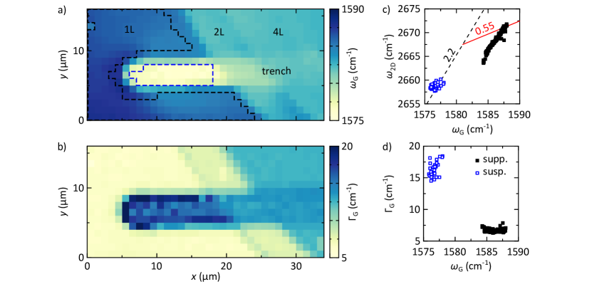
The graphs in Fig. S1c and d correlate with and , respectively. The data are extracted from the delimited areas on the map in Fig. S1a and plotted as open blue squares for the suspended area and filled black squares for the supported area. On Fig. S1c the data are concentrated with a small standard deviation and line up along a slope of . Here we use the reference point ( cm-1, cm-1), as in ref. Metten et al. (2013) for neutral, unstrained suspended graphene at K and for a laser wavelength of 532 nm. In contrast, the data of the supported area are aligned along a line with the same slope of 2.2 but shifted to a higher due to substrate-induced doping. Following the vector decomposition model proposed by Lee et al. Lee et al. (2012a) and applied to our suspended sample, we might estimate an average tensile strain of % and a doping level cm-2. The latter is in stark contrast with the doping level of the supported part, which is of one order of magnitude larger. The data represented in Fig. S1d combine the two maps in Fig. S1a and b, and confirm the quasi-undoped character of the membrane by the two well-distinguishable areas in the --plane Lazzeri and Mauri (2006); Berciaud et al. (2009).
SI 3 Raman enhancement due to optical interferences
The trench on which graphene is exfoliated and suspended can be considered as a multilayered system, i.e. [Si - SiO2 - air/vacuum - graphene - air/vacuum]. The involved layer thicknesses are on the same order of magnitude as the wavelength of the light, so that optical interference effects come into play. We model the evolution of the ratio of the incoming and scattered electrical field with a Fabry-Pérot calculation, according to
| (S1) |
Here, are the reflection coefficients at the interface and the phase is defined as . The Raman interaction takes place in the last (graphene) layer and has to be considered separately. Multiple reflections within the graphene layer for the incoming (laser) and Raman-scattered light are calculated by taking the effective reflection coefficient (on one side of the graphene membrane). An optical enhancement factor is then obtained by integrating over the thickness of the membrane Blake et al. (2007); Yoon et al. (2009) according to
| (S2) |
where is the electric field of the incoming laser beam, the electric field of the incoming laser beam at the position where the Raman interaction takes place, the Raman electric field created at and the Raman electric field coming out of the layered system. The enhancement factor is generally normalized relative to the case of monolayer graphene in free space. Here, for a clearer comparison with our experimental data (see Fig. 2a and 2b in the main text), we renormalize the amplitude of the enhancement factor variations (between its minimal and maximal values) by the measured ratio between the minimal and maximal integrated Raman intensities we have observed experimentally. This renormalization has no significant consequence on the determination of the membrane deflection.
SI 4 Details on the electromechanical model
The deflection is modeled by regarding the electrostatic pressure on the membrane, which writes
| (S3) |
is the deflection profile perpendicular to the trench ( direction), the dielectric constant, the relative dielectric constant of SiO2 and the residual oxide thickness.
The membrane deflection in the middle of the trench (simply denoted in the main manuscript), induced by a uniform pressure load writes Medvedyeva and Blanter (2011); Bao et al. (2012)
| (S4) |
where is the Young’s modulus, the Poisson ratio and the thickness of the membrane, the width of the trench (see Fig. 1b in the main text) and its pre-strain (in N/m). As mentioned in the main text, the scaling is well-known for membranes (without bending rigidity) Hencky (1915); Komaragiri et al. (2005); Yue et al. (2012); Metten et al. (2014), and the additional pre-strain-term can be interpreted as an effective bending rigidity moderating the deflection, as scales linearly with for thin plates Landau and Lifshitz (1970); Vlassak and Nix (1992); Beams (1995); Williams (1997); Medvedyeva and Blanter (2011).
| (S5) |
by supposing a parabolic profile of the membrane, and where is the total strain in the membrane, with the strain due to the electrostatically induced deflection. The profile is taken as , which is a first approximation, because back coupling mechanisms between the deflection and the charge redistribution within the membrane are neglected. However, Eq. (S5) can be self-consistently solved considering a parabolic profile.
As discussed in the main text, Eq. (S4) requires a uniform pressure load over the membrane, which is calculated as an average value of , obtained by integrating the local capacitance along the parabolic profile :
| (S6) |
with , and the distance between the SiO2 layer and the membrane, is the vacuum permittivity and is the DC dielectric constant of SiO2. We can thus compute as a function of by injecting Eq. (S6) into Eq. (S4):
| (S7) |
Here, and the pre-strain can be used as a fitting parameter, as shown in Fig. 3a in the main text. Equation S7 is solved numerically.
SI 5 Deflection extracted from
The values of presented in Fig 3a of the main manuscript are derived from the integrated intensity of the G-mode feature . In Fig. S2 we show the data extracted from and the corresponding fit using our electromechanical model. A pre-strain of N/m is found, which is comparable the one extracted from .
SI 6 Electromechanical calculations for various SiO2 thickness
Commonly used Si/SiO2 substrates have oxide thickness of and nm. In Fig. S3, we show data similar to Fig. 3b-c in the main manuscript for for m and m, respectively.
SI 7 Critical charge carrier density
SI 8 Scanning Electron Microscopy (SEM) imaging