First-principles Study on Structural, Thermal, Mechanical and Dynamic Stability of T’-MoS2
Abstract
Using first-principles density functional theory calculations, we investigate the structure, stability, optical modes and electronic band gap of a distorted tetragonal MoS2 monolayer (T’-MoS2). Our simulated scanning tunnel microscopy (STM) images of T’-MoS2 are dramatically similar with those STM images which were identified as Kx(H2O)yMoS2 from a previous experimental study. This similarity suggests that T’-MoS2 might have already been observed in experiment but was unexpectedly misidentified. Furthermore, we verify the stability of T’-MoS2 from thermal, mechanical and dynamic aspects, by ab initio molecular dynamics simulation, elastic constants evaluation and phonon band structure calculation based on density functional perturbation theory, respectively. In addition, we calculate the eigenfrequencies and eigenvectors of the optical modes of T’-MoS2 at point and distinguish their Raman and infrared activity by pointing out their irreducible representations using group theory; at the same time, we compare the Raman modes of T’-MoS2 with those of H-MoS2 and T-MoS2. Our results provide a useful guidance for further experimental identification and characterization of T’-MoS2.
pacs:
68.37.Ef, 63.20.dk, 63.22.-m, 78.20.EkI Introduction
The successful fabrication of two-dimensional (2D) materials such as graphene have aroused intense interest due to their intriguing electronic, mechanical, optical, and thermal properties.Novoselov et al. (2005); Zhang et al. (2005) The gapless nature of graphene, however, presents limitations to their potential application in industry.Liao et al. (2010); Schwierz (2010) Therefore, the interest of study has gradually turned to other 2D material such as transition metal dichalcogenides (TMD) monolayer. TMD generally have diverse crystal structures which can provide significantly different electronic properties varying from semiconducting to metallic.Mak et al. (2010); Wu et al. (2011); Kan et al. (2014); Li et al. (2014)
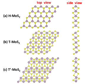
The most common TMD is MoS2, which has three possible phases. They are H-MoS2Wang et al. (2012),T-MoS2Py and Haering (1983); F. Wypych and Prins (1998); Ataca, Sahin, and Ciraci (2012) and T’-MoS2,Py and Haering (1983); Kan et al. (2014) as displayed in Fig.1 respectively. H-MoS2, i.e., the 2D trigonal prismatic phase, being the most stable configuration under normal conditions,Benavente et al. (2002) can be exfoliated from the bulk 2H phase (P6/mmc) using a mechanical methodWang et al. (2012) or be synthesized with vapor depositionLee et al. (2012) It is a semiconductor with a direct band gap of 1.8 eV.Qin et al. (1991); Radisavljevic et al. (2011) T-MoS2 (tetragonal symmetry, octahedral coordination) phase can be synthesized from solvent based exfoliation method. It is reported to be metallic and can be used as an electrode material.Kappera et al. (2014) Although T-MoS2 was observed in experiment,Lin et al. (2013); Kappera et al. (2014) the stability of T-MoS2 is still a controversial issue. For example, density functional theory (DFT) calculations predict that the free standing T-MoS2 is unstable, since the seriously imaginary frequency presented in its phonon dispersion relation.Shirodkar and Waghmare (2014); Singh, Shirodkar, and Waghmare (2015)
Qin et al. performed an STM study on the surface of restacked MoS2 and observed a new superstructure characterized by the formation of zigzag chains.Qin et al. (1992) Then, an electron crystallography study also suggested that the restacked MoS2 is more like WTe2 with zigzag Mo-Mo chains.Heising and Kanatzidis (1999) This zigzag phase is called the distorted tetragonal MoS2, labeled as T’-MoS2 in the present paper, which was also referred to as the 1T’ phase or ZT-MoS2 phase in other theoretical study.Py and Haering (1983); Kan et al. (2014) T’-MoS2 is thought to be a charge density wave (CDW) state as a result of the Piers phase transition from T phase.Whangbo and Canadell (1992) The structural stability of T’-MoS2 was first inferred from formation energy by Kan et al..Kan et al. (2014) They found that the formation energy of T’-MoS2 is higher than that of H-MoS2 but lower than T-MoS2. Namely, T’-MoS2 is a meta-stable phase. Qian et al. calculated the phonon band structure of T’-MoS2 and found no imaginary frequency, which confirmed the vibrational stability of T’-MoS2.Qian et al. (2014) As to the stability of T’-MoS2 in other physical respects, such as the thermal and mechanical stability, however, has not been studied theoretically by far, to the best of our knowledge. Although previous experimental study has reported the observation of T’-MoS2 phase identified by experimental STM images,Eda et al. (2012); Guo et al. (2015) those STM images, however, have not been sufficiently explicit to demonstrate the existence of T’-MoS2. In addition, a discrepancy is also presented with respect to the band gap of T’-MoS2. For instance, T’-MoS2 is first predicted to be a semiconductor with a narrow band gap.Kan et al. (2014); Qian et al. (2014) In contrast, the electronic band structure given by Gao et al. implied that T’-MoS2 was a semimetal.Gao et al. (2015)
Therefore, a theoretical study on the physical stability and electronic properties of T’-MoS2 is necessary and urgent. In the present work, we perform density functional theory (DFT) calculations within local density approximation (LDA) to investigate the simulated STM images, stability and the electronic band gap of T’-MoS2. The simulated STM images provide a significant reference for identifying the lattice structure from experimental STM images. The ab initio molecular dynamics (AIMD) simulations confirm the thermodynamic stability of T’-MoS2 at room temperature; the calculating results of elastic constants meet the Born-Huang criteria, which implying the mechanical stability of T’-MoS2; the absence of the imaginary frequency in the phonon dispersion relation indicates the vibrational stability of T’-MoS2. Besides, we also classify the optical modes by group theory and compute their corresponding eigenfrequency and eigenvector, which play an important role in the identification and characterization of T’-MoS2 phase from optical experiment. Moreover, we make a contrast calculation of the electronic band structure to determine the effect of the spin-orbit coupling, which clarifies the origin of band gap of T’-MoS2.
The remainder of this paper is organized as follows. In Sec. II, methodology and computational details are described. Sec. III presents first the simulation of STM imaging of MoS2 in three different phases, then the stability of T’-MoS2 is explored from different aspects. The symmetry classification of the vibrational modes along with their eigenfrequency and eigenvector are calculated. Furthermore, the electronic band structure and band gap of T’-MoS2 are investigated by considering the spin-orbit coupling. Finally, conclusions are drawn in Sec. IV.
II Methodology
Both total energy and electronic band structure calculations were performed by using the Vienna ab initio simulation package (VASP).Kresse and Furthmüller (1996a, b) The electron-ion interaction was described by using the frozen-core projector augmented wave (PAW) method;Blöchl (1994); Kresse and Joubert (1999) the exchange and correlation were treated with generalized gradient approximation (GGA) in the Perdew-Burke-Ernzerhof (PBE) form.Perdew, Burke, and Ernzerhof (1996) Besides standard DFT with GGA, the hybrid Heyd- Scuseria-Ernzerhof (HSE)06 method,Heyd, Scuseria, and Ernzerhof (2003, 2006) was also employed to give a more accurate description of the band gap of T’-MoS2. In the HSE06 method, a fraction of the exact screened Hartree-Fock (HF) exchange is incorporated into the PBE exchange using a mixing parameter = 0.25. We used a cutoff energy of 300 eV for the plane wave basis set, which yields total energies convergence better than 1 meV/atom. The Van der Waals interactions are treated with the empirical correction scheme of Grimme’s DFT-D2 method, which has been successful in describing the geometries of various layered materials.Grimme (2006); Bučko et al. (2010)
In the slab model of single-layer MoS2, the periodic slabs were separated by a vacuum layer of 15 Å in the c direction to avoid mirror interactions. A 10×5×1 k-mesh including -point, generated according to the Monkhorst-Pack scheme,Monkhorst and Pack (1976) was applied to the Brillouin-zone (BZ) integrations. Through geometry optimization, both the shapes and internal structural parameters of pristine unit-cells were fully relaxed until the residual force on each atom is less than 0.01 eV/Å.
To examine the stability of the modeled structure of T’-MoS2 from the lattice dynamics point of view, the force-constant approach involving a finite displacement was adopted as employed by the PHONOPYTogo and Tanaka (2015) code. The force constant matrix was calculated with a 7×4×1 supercell containing 168 atoms, based on the density functional perturbation theory (DFPT) method Gonze and Lee (1997) implemented into VASP. Furthermore, the phonopy codes also enable us to obtain the eigenfrequency and eigenvector of lattice vibrational modes at the center of BZ.
The simulated STM images were generated by using the P4VASP package, which can facilitate the simulation of STM image with a continuously varying scanning distance. The theory for simulating STM imaging by ab initio density functional calculations is well established.Tománek and Louie (1988) Giving a small bias voltage between the sample and the STM tip produces a tunneling current, whose density can be obtained from a simple extension Selloni et al. (1985) of the expression derived by Tersoff and Hamann Tersoff and Hamann (1983, 1985):
| (1) |
where
| (2) |
and
| (3) |
Here, is the local density of states at the center of the tip at and are the electron eigenstates of the unperturbed surface at energy . These eigenstates are commonly represented by Kohn-Sham eigenstates obtained using DFT. The assumptions behind this is that the relevant tip states are described by waves with a constant density of states.Tersoff and Hamann (1983); Selloni et al. (1985); Tersoff and Hamann (1985) Furthermore, the tunneling matrix element is considered to be independent of both the lateral tip position for a constant tip-to-surface distance and the bias voltage in the narrow (but nonzero) energy region . Equation 3 describes tunneling from occupied states of the sample to the tip. The simulated STM image is not sensitive to the bias voltage as long as the valence band enters in the integral range, but sensitive to the scanning distance from the tip to the sample surface.
The simulating STM imaging has been used for studying the modification of the electronic structure of the 2H phase MoS2 (0001) surface produced by several point defects.Fuhr, Saúl, and Sofo (2004) Recently, it was also used for exploring the few-layer phosphorus capped by graphene and hexagonal boron nitride monolayer.Rivero et al. (2015) In present work, we apply this method to study the structure of single-layered MoS2. Different bias voltage are used for distinct phases of monolayer MoS2 according to their electronic properties. For H-MoS2, its band gap is 1.7 eV, and its Fermi level is under the conductor band at about 0.1 eV, so that the value of bias voltage is set to 1.8 V, and thus the energy range enters the valence band at about 0.2 eV. As to metallic T’-MoS2, we have compared the simulated images using two different bias voltage (0.3 and 1.8 V) but find no significant distinction, hence we always use the smallest one in the following calculation. For T’-MoS2, its band gap is merely 0.1 eV, so a bias voltage =0.5 V is enough.
III Results and discussion
III.1 Simulated STM images and Identification of Monolayer MoS2
We begin our discussion by comparing the simulated STM images of the three possible structures, namely, H, T, and T’ phases of monolayer MoS2.Chhowalla et al. (2013) The lattice structures of the three phases are displayed in Fig. 1. The most energetically favorable H-MoS2 (as shown in Fig. 1(a)) has a sandwich-like structure of three planes of 2D hexagonally packed atoms, S-Mo-S, where Mo atoms are trigonal-prismatically coordinated by six S atoms, forming ABA stacking with P6m2 space-group symmetry. In contrast, the Mo atoms in the T-MoS2 (as shown in Fig. 1(b)) structure are octahedrally coordinated with the nearby six S atoms, resulting in ABC stacking with P3m1 space group symmetry. H- and T-MoS2 phase have very different electronic properties: the former is a large gap semiconductor but the latter a metal. It has been predicated that the T-MoS2 is typically unstable in free-standing conditionShirodkar and Waghmare (2014); Kan et al. (2014). T-MoS2 should undergo the Piers distortion in one direction to form a super-lattice structure, consisting of one-dimensional zigzag Mo-Mo chains along the other direction, i.e., the T’-MoS2 phase, as shown in Fig. 1(c). It implies theoretically that T’-MoS2 should be more stable than T-MoS2 in free-standing conditions. In experiments, however, Eda et al. have observed both T- and T’-MoS2 by scanning transmission electron microscopy (STEM) imaging,Eda et al. (2012) but the image of T’-MoS2 is not so clear as that of T-MoS2. Although WS2 and MoTe2 monolayer have been found experimentally.Mahler et al. (2014); Keum et al. (2015) T’-MoS2, has not been identified unanimously in experiment yet, to the best of our knowledge. Therefore, we perform an ab initio density functional calculations to simulate STM images of MoS2 monolayer in the three phases. Figure.2 shows the calculated STM images of H-, T-, as well as T’-MoS2, respectively. Our simulated STM images agree well with those images obtained in previous experiments.Eda et al. (2012) This agreement indicates the reliability of the simulated STM imaging method.
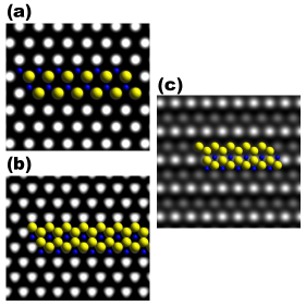
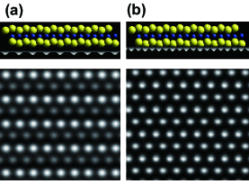
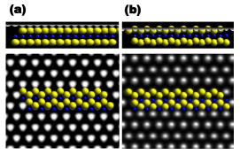
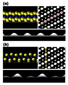
The scanning distance represents the distance form scanning plane to referring plane, and the referring plane is put on the upper surface of crystal cell in slab model of MoS2 monolayer. The scanning distance is denoted in term of the tip position in P4VASP. To determine the influence of the scanning distance on STM imaging, we perform the simulating STM imaging calculations varying continuously with scanning distance. It is found that the simulated STM images vary remarkably with the scanning distance. This variation even may lead to misidentification of the experimental STM images.Altibelli, Joachim, and Sautet (1996) On one hand, it means that we may obtain quite different STM images actually belonging to the identical structure in experiment, as seen in Fig. 3, in which we have shown the top and side view of two different scanning distances, while the tip position for the middle plane of the MoS2 monolayer is . Then the distances from scanning plane to the middle plane are and , respectively. If merely judging from the top view of the simulation images without referring the other information, you must think that the lower sublet of Fig. 3(a) represents T’-MoS2 phase but that of Fig. 3(b) belongs to the image of T-MoS2. On the other hand, it also means that the different phases of MoS2 may have similar STM images. Comparing the simulated images of T-MoS2 and T’-MoS2 with appropriate scanning distances presented in Fig. 4, you may find it is hard to distinguish these two phases. Thus, we should not make identification only by single experimental STM image without any other information.
Knowing this how can we identify the lattice structure of STM image in experiment? The method is to scan the STM images while varying with tip-to-surface distance. By comparing and contrasting those images, you can make the correct identification, for the different structures have distinct changing patterns. This suggestion is deduced from our STM imaging simulation of T-MoS2 and T’-MoS2 with continuously varying scanning distance. The structural symmetry of simulated image of T-MoS2 remains invariant as the scanning distance varies consecutively, in contrast, that of T’-MoS2 is varying significantly, just as demonstrated in Fig.3. It is worth mentioning that the STM images obtained experimentally are usually scanning within one or two given tip-to-surface distance. Then a question arises: whether it is possible that the structure of MoS2 observed in previous experiments could be T’ phase rather than T phase?
It is natural to examine the relevant experiments in literature, and we find that the answer is affirmative. In an experimental STM imaging study of T-MoS2F. Wypych and Prins (1998), there are several STM images in Figures 2 and 3 in Ref[F. Wypych and Prins, 1998], which were identified as Kx(H2O)yMoS. We make the corresponding simulation of T’-MoS2, which are shown in Fig. 5. Compare our simulated STM images of T’-MoS2 phase with these images, we find that the simulated images surprisingly accord with the experimental STM images. This dramatic accordance indicates strongly that these experimental images should be corresponding to T’-MoS2 phase rather than Kx(H2O)yMoS2. That is to say, the T’-MoS2 has been synthesized accidentally but misidentified unfortunately. If this was true, it actually means an experimentally feasible method for synthesizing T’-MoS2, which is important for the fabrication of a novel topological field effect transistor.Qian et al. (2014)
The instability of free standing T-MoS2 at 0 K is revealed by imaginary frequency presented in its phonon dispersion relations from the recent first-principles calculations.Shirodkar and Waghmare (2014); Singh, Shirodkar, and Waghmare (2015) At the same time, several theoretical and experimental researches show that the function of alkali metal is to offer an extra electron to make the T-MoS2 phase more stable in energy.Kappera et al. (2014) While in Ref. [F. Wypych and Prins, 1998], the presence of water stabilizes the T’ phase from the original high symmetric structure.Qin et al. (1991); Yang et al. (1991); Qin et al. (1992); Gordon et al. (2002). Therefore, the method designed to obtain T-MoS2 is actually a feasible method to produce T’-MoS2 in experiment. For reliably identifying T’-MoS2 in experiment, it is necessary to exploit the otherwise stability of T’-MoS2.
III.2 Thermal stability of T’-MoS2
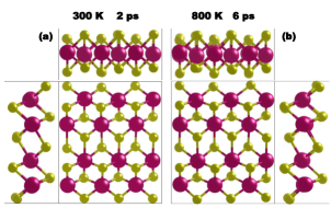
The thermal stability of T’-MoS2 is explored by performing AIMD simulations using canonical ensemble. To reduce the constraint of periodic boundary condition, the T’-MoS2 is simulated by () super-cells. The snapshots of T’-MoS2 atomic configurations for the final stages of AIMD simulations at 300 K and 800 K are shown in Fig. 6 (a) and (b), respectively. One can find that no significantly reconstruction are observed at 300 K and 800 K. Here the only exception in the latter case is that the S and Mo atoms are found to be slightly moved due to thermal fluctuation. This means that T’-MoS2 can withstand the higher temperature at least up to 800 K, implying the high-energy barriers between T’ phase and H phase, which is in consistent with the first-principles calculations performed by Qian et al.Qian et al. (2014)
III.3 Mechanical Stability and Anisotropy of T’-MoS2
Since the super-cell is fixed during the MD simulations, we have to evaluate the effect of elastic distortion on structural stability. In order to guarantee the positive-definiteness of strain energy following lattice distortion, the components of linear elastic modulus tensor of a stable crystal must obey the Born-Huang criteria Ding and Wang (2013). We calculate the change of energy due to the in-plane strain to examine the mechanical stability of T’-MoS2. For a 2D crystal, the elastic strain energy per unit area can be written asWang et al. (2015a)
| (4) |
where are the components of the elastic modulus tensor using the standard Voigt notation ( i.e., 1-xx, 2-yy, and 6-xy),Andrew et al. (2012) corresponding to second partial derivative of elastic energy with respect to strain. The elastic constants can be derived by fitting the energy curves associated with uniaxial and equi-biaxial strains. Under uniaxial strain applied along x direction, , this leads to . Parabolic fitting of the uniaxial strain curve yields GPanm. Similarly, under uniaxial strain applied along y direction, is derived to be 124.0 GPanm. Under equi-biaxial strain, , one have . By fitting the equi-biaxial strain curve, we obtain GPanm, which means that GPanm. For a mechanically stable 2D crystal, the elastic constants should satisfy two criteria: and .Ding and Wang (2013)For T’-MoS2, one can easily verify that the calculated components of the elastic modulus tensor satisfy ; besides, the calculated =38.8 GPanm is positive. Both the two criteria of mechanical stability are met, thus the mechanical stability of T’-MoS2 is confirmed.
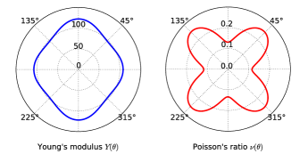
Due to its lower point group symmetry, T’-MoS2 has anisotropic elastic property, which is significantly different from H- and T-MoS2. Both H- and T-MoS2 are of isotropic elastic properties described by two elastic constants: Young’s modulus and Poisson’s ratio . The Young’s modulus and Poisson’s ratio of T’-MoS2, however, do not remain constant, but vary with orientation. The formula for Young’s modulus and Poisson’s ratio areDing and Wang (2013); Wang and Geng (2016)
| (5) | |||
| (6) |
where and , is the the angle with respect to the x-axis. The above two formulas are universal for all orthogonal 2D crystal.
Their extremum directions can be determined by analyzing the zeros of the first derivative of and . Generally, there are three extremum directions for both and , in which there are two same extremum conditions: and , which means that the coordinate axes directions x and y (rather, the symmetrical principal axes directions) are extremum directions. we find that for , both the two axes may maximum (or minimum) directions, meanwhile, for , they must be both minimum (or maximum) directions. Certainly, the two maximum (or minimum) directions mean that there must be one minimum (or maximum) direction between the two axes. Depending on the relative value of elastic constants, the third extremum between the two axes for may not exist, then one axis direction is maximum and the other minimum direction. For Poisson’s ratio, the third extremum always exists, except for isotropic case. The above conclusions about extremum direction are also universal for orthogonal 2D crystal structures.
Here, we plot the curves of and in polar coordinates for T’-MoS2 in Fig 7, which intuitively show the elastic anisotropy of T’-MoS2. First, it can be seen that the extremum directions are consistent with our analyses above. Second, it can be found that the variation range of Young’s modulus is from about 96.9 to 124.0 GPanm, the value of Poisson’s ratio is limited between 0.117 and 0.25. Third, it can be found that the principal minimum direction of is along and the maximum direction of for T’-MoS2 are almost along diagonal direction.
III.4 Lattice Dynamic Stability and Vibrational Modes of T’-MoS2
III.4.1 Lattice dynamic stability
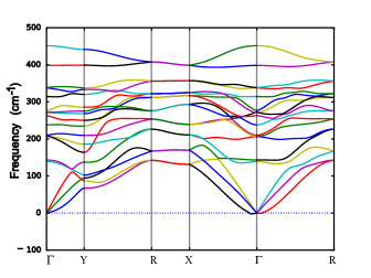
To further verify the lattice dynamic stability of the T’-MoS2, we calculate phonon dispersion relation of T’-MoS2 and demonstrate it in Fig. 8. we can note that the phonon dispersion of T’-MoS2 has three acoustic and fifteen optical branches. The three acoustic branches are the in-plane longitudinal acoustic (LA), the transverse acoustic (TA), and the out-of-plane acoustic (ZA) branches. The LA and TA branches have linear dispersion and a higher frequency than the ZA mode around point in the Brillouin zone. In contrast to H-MoS2,Jiménez Sandoval et al. (1991); Molina-Sánchez and Wirtz (2011) there is no band gap between acoustic branches and optical branches. All the rest of vibrational branches along other lines in BZ are non-degeneracy, except the vibrational branches along R–X line at the boundary of BZ, which are two order degeneracy. The lifting of degeneracy of vibrational branches reveals the Piers phase transition from a high symmetric structure. The absence of the imaginary frequency throughout the 2D BZ indicates the structural stability of the T’-MoS2. Our results are in good agreement with those obtained in Ref [Qian et al., 2014].
III.4.2 Symmetric analysis of lattice vibrational modes
Both laser Raman scattering and Infrared absorption spectra are powerful tools for structural identification and characterization of 2D materials. To guide the optical spectra study in future experiment, we deduce the symmetry classification of phonon modes at the point by using group theory, and further point out R and IR activity of the optical modes. The unit cell of T’-MoS2 consists of two S-Mo-S units with a total of six atoms, suggesting that there are eighteen phonon modes (three acoustic and fifteen optical modes) at the point. Lattice vibrations can be classified based on the irreducible representation of space group.Dresselhaus, Dresselhaus, and Jorio (2007) The space group of T’-MoS2 is (or , No.11), whose factor group is isomorphic with the point group . The character table for point group is given in Table 1,
| 1 | 1 | 1 | 1 | |||
| 1 | -1 | -1 | 1 | |||
| 1 | 1 | -1 | -1 | |||
| 1 | -1 | 1 | -1 |
where , , and are signs of one-dimensional irreducible representations; and are used when the character of the major rotation operation is 1 or -1, respectively; the subscripts and denote representations that are symmetric and antisymmetric with respect to the inversion operation if the point group has a center of inversion symmetry; , , and are components of polar vectors. From Table 1, we note that T’-MoS2 has no two-dimensional irreducible representations, i.e., there is no degenerate optical modes at the center of BZ, which distinctively differs from that of H- and T-MoS2.Wieting and Verble (1971); Jiménez Sandoval et al. (1991); Cai et al. (2014); Zhang et al. (2015)
| 3 | -1 | 1 | -3 | |
| 6 | 0 | 6 | 0 | |
| 18 | 0 | 6 | 0 |
We classify the lattice vibrational modes of T’-MoS2 at by group theory according to the irreducible representations of C2h. Characters of atomic displacement vector representations, primitive cell equivalent representations, and lattice vibration representations of T’-MoS2 are shown in Table 2. These representations can be reduced into the irreducible representations summarized in Table 1:
| (7) | ||||
| (8) | ||||
| (9) |
where , , and are the symmetry representations of atomic displacement vector, the equivalent representations of the primitive cell and the symmetry representations of lattice vibration at the zone center of BZ, respectively. The symmetry representation of lattice vibration is equal to the direct product of the symmetry representations of atomic displacement vector and the equivalent representations of the primitive cell.Dresselhaus, Dresselhaus, and Jorio (2007)
This symmetry representation of lattice vibration includes eighteen phonon modes entirely and can be further decomposed into the representations of acoustic and optical modes as follows:
| (10) | ||||
| (11) |
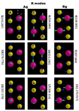
where the acoustic modes include one and two modes, all their frequencies are identical to zero; the rest of the fifteen nonzero frequency modes belong to optical modes. The six optical modes of odd parity (2 and 4) are IR active, the other nine optical modes of even parity (6 and 3) are R active. The R and IR modes are mutually exclusive in T’-MoS2 phase because of the presence of inversion symmetry in the crystal. It is also worth pointing out that the above symmetry analyses is suitable for all T’ phase of 2D TMD, namely, T’-MX2 with M=(Mo, W) and X=(S, Se, and Te). For easy identifying T’-MoS2 from a Raman optical spectral experiment, we compare the R modes of T’-MoS2 with those of H- and T-MoS2.Cai et al. (2014); Zhang et al. (2015) It can be found that both H and T phase of MoS2 have two-dimensional ( and ) modes, while T’ phase has only one-dimensional modes, no two-dimensional mode. This means that if one detects the mode in a Raman optical spectral experiment on a MoS2 monolayer, it coud not be in T’ phase. In addition, since the presence of inversion symmetry both in atomic structures of T- and T’-MoS2, according to exclusion principle, the R modes in these two phase must be modes, where T phase has both one- and two-dimensional modes ( and ) but T’ phase has only one-dimensional modes ( and ). In H-MoS2, however, there is no inversion symmetry and thus no or mode. Thus, we may draw the conclusion that if one finds some one-dimensional but no two-dimensional R modes of symmetry in a Raman optical spectral experiment on a MoS2 monolayer, then this MoS2 monolayer is probable in T’ phase.
III.4.3 Eigenfrequency and eigenvector of optical modes
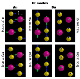
For comparing quantitatively with optical spectra experiments, we compute the eigenfrequency of the fifteen optical modes by phonopy. In Table 3, the fifteen optical modes with frequency are grouped by their irreducible representations and optical activity, where bold Arabic numbers represent the optical modes, which ordering are according to their frequencies from low to high. T’-MoS2 structure can be identified and characterized based on Table 3 in future optical spectra experiments.
| Raman modes | Infrared modes | ||
|---|---|---|---|
| 5(143.267) | 4(138.905) | 8(210.225) | 9(238.132) |
| 6(206.684) | 7(207.684) | 12(271.867) | 10(262.733) |
| 13(276.776) | 11(270.917) | 16(338.798) | |
| 14(314.290) | 18(451.503) | ||
| 15(337.570) | |||
| 17(398.414) | |||
Besides, the vibrational eigenvector of the IR and R modes are also illustrated in Fig. 9 and Fig. 10. For IR modes, as can be seen in Fig. 9, both the two modes 8(210.225) and 12(271.867) are vibrating along in-plane directions, while only one mode 18(451.503) which is of the highest frequency, vibrates perpendicular to crystal plane. For IR modes, from Fig. 10 we find that all the three modes 4(138.905), 7(207.684) and 11(270.917) are in-plane vibrations, while none of the six modes is vibrating along purely in-plane or out-plane direction. The vibration direction of IR and R active modes is vital for setting the incident and detection directions as well as the polarization of the light used in optical spectra experiments.
III.5 The Electronic Band Gap of T’-MoS2
There has been a discrepancy about the band gap of T’-MoS2 presented in recent literature.Kan et al. (2014); Qian et al. (2014); Gao et al. (2015) Kan et al. performed spin-polarized DFT calculations with GGA-PBE and with HSE06 to investigate the band structure of monolayer of T’-MoS2. They pointed out that the structural distortions of ZT-MoS2 lead to the opening of a direct gap of 0.022 or 0.23 eV. The band gap obtained by DFT with GGA-PBE is significantly different from that obtained with HSE06, the latter is ten times greater than the former.Kan et al. (2014) Qian et al. later found that 1T’-MoS2 (i.e., T’-MoS2) was a semiconductor with a band gap of 0.1 eV based on many-body perturbation theory within the GW approximation.Qian et al. (2014) However, Gao et al.’s calculation by DFT based on Dmol3 software showed that T’-MoS2 was a semiconductor with a very narrow band gap of 0.006eV.Gao et al. (2015) Generally speaking, the band gap is underestimated by GGA-PBE but overestimated by HSE06.Thus, the band gap of 0.1 eV obtained by Qian et al.Qian et al. (2014) should be closer to the real value since this value is in between the two results: 0.022 eV and 0.23 eV, where the former is calculated by DFT with GGA-PBE and the latter is with HSE06. As to the band gap of 0.006 eV Gao et al. (2015), it may seriously underestimate the band gap since it is far lower than the underestimated result 0.022 eV.
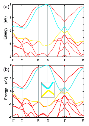
To examine our inference, we calculate the electronic band structure of T’-MoS2 by DFT with GGA-PBE to explore the effect of spin-orbit coupling. Fig. 11 shows the electronic band structure of T’-MoS2 without (a) and with (b) the consideration of the spin-orbit coupling. Comparing Fig. 11(a) and 11(b), one can find that the electronic band dispersion curves in the two cases are almost as the same in general, but the crucial difference in detail occurs near the Fermi line. In the former case, there seems no band gap, while in the latter case, the band gap does present, and is equal to 0.048 eV. This result implies that it is the spin-orbit coupling opens or widens out the band gap. Besides, we also find that the band structure without consider the spin-orbit agrees well with that of Gao et al.’s especially in the vicinity of the Fermi line.
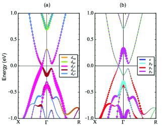
To determine whether there exists a very small band gap without spin orbital interaction, we plot the orbital-projected band structuresWang et al. (2015b) of Mo and S atom around the point without considering spin-orbit coupling. As can be seen in Fig. 12, for both Mo and S atom, the two bands meeting at the Fermi lime cross each other directly without any avoiding.This direct crossing shows that there is exactly no band gap existing in electronic band structure of T’-MoS2 if the spin-orbit interaction is neglected. Thus, we can conclude that the interaction which lifting the degeneracy of electron states at the Fermi line and opening the band gap is the spin-orbit coupling. In addition, we recalculate the electronic band structure of T’-MoS2 by DFT with HSE06 and the obtained band gap is about 0.153 eV, which falls in between those obtained in Refs [Kan et al., 2014 and Qian et al., 2014]. Thus far, we come to conclusion that T’-MoS2 must be a semiconductor of a narrow gap, while Gao et al.’s calculation may have not included the spin-orbit interaction.
IV Conclusions
In conclusion, we have performed first-principles investigation on the structure, physical stability, optical modes and electronic band gap of T’-MoS2. Our simulated STM images of MoS2 monolayer are in good agreement with previous experimental results. Moreover, we have found unexpectedly that the simulated STM images of T’-MoS2 vary significantly with the scanning distance. This variation should be considered in the structural identification from experimental STM images. Furthermore, the dramatic similarity between the simulated STM images of T’-MoS2 with that of earlier experimental study means that T’-MoS2 may have been observed in experiment but was mistaken for the intercalation compound Kx(H2O)yMoS2. If so, T’-MoS2 should be stable in structure. To verify its physical stability, the thermal and mechanical stability of T’-MoS2 have explored by AIMD simulations and elastic constants fitting and the results are affirmative. In addition, the lattice dynamic stability of T’-MoS2 is also confirmed by the absence of imaginary frequency in our phonon dispersions relations. Therefore, the physical stability of T’-MoS2 has been verified finally. Besides, we have made symmetry classification of optical modes and calculated their eigenfrequencies and eigenvectors, which provides an important guidance for further optical spectral study in experiments. Future work will investigate the intensity of R and IR spectra theoretically.
Acknowledgements.
Y. C. Liu is thankful to H. B. Niu for his help on first principles calculations. V.Wang. acknowledges the financial support of The Special Scientific Research Program of the Education Bureau of Shaanxi Province, China (Grant No. 15JK1531).References
- Novoselov et al. (2005) K. Novoselov, A. K. Geim, S. Morozov, D. Jiang, M. Katsnelson, I. Grigorieva, S. Dubonos, and A. Firsov, Nature 438, 197 (2005).
- Zhang et al. (2005) Y. Zhang, Y.-W. Tan, H. L. Stormer, and P. Kim, Nature 438, 201 (2005).
- Liao et al. (2010) L. Liao, Y.-C. Lin, M. Bao, R. Cheng, J. Bai, Y. Liu, Y. Qu, K. L. Wang, Y. Huang, and X. Duan, Nature 467, 305 (2010).
- Schwierz (2010) F. Schwierz, Nat. Nanotechnol. 5, 487 (2010).
- Mak et al. (2010) K. F. Mak, C. Lee, J. Hone, J. Shan, and T. F. Heinz, Phys. Rev. Lett. 105, 136805 (2010).
- Wu et al. (2011) Y. Wu, Y.-m. Lin, A. A. Bol, K. A. Jenkins, F. Xia, D. B. Farmer, Y. Zhu, and P. Avouris, Nature 472, 74 (2011).
- Kan et al. (2014) M. Kan, J. Y. Wang, X. W. Li, S. H. Zhang, Y. W. Li, Y. Kawazoe, Q. Sun, and P. Jena, J. Phys. Chem. C 118, 1515 (2014).
- Li et al. (2014) W. Li, M. Guo, G. Zhang, and Y.-W. Zhang, Phys. Rev. B 89, 205402 (2014).
- Wang et al. (2012) Q. H. Wang, K. Kalantar-Zadeh, A. Kis, J. N. Coleman, and M. S. Strano, Nat. Nanotechnol. 7, 699 (2012).
- Py and Haering (1983) M. Py and R. Haering, Can. J. Phys. 61, 76 (1983).
- F. Wypych and Prins (1998) T. W. F. Wypych and R. Prins, Chem. Mater. 10, 723 (1998).
- Ataca, Sahin, and Ciraci (2012) C. Ataca, H. Sahin, and S. Ciraci, J. Phys. Chem. C 116, 8983 (2012).
- Benavente et al. (2002) E. Benavente, M. Santa Ana, F. Mendizábal, and G. González, Coord. Chem. Rev. 224, 87 (2002).
- Lee et al. (2012) Y.-H. Lee, X.-Q. Zhang, W. Zhang, M.-T. Chang, C.-T. Lin, K.-D. Chang, Y.-C. Yu, J. T.-W. Wang, C.-S. Chang, L.-J. Li, and T.-W. Lin, Adv. Mater. 24, 2320 (2012).
- Qin et al. (1991) X. R. Qin, D. Yang, R. F. Frindt, and J. C. Irwin, Phys. Rev. B 44, 3490 (1991).
- Radisavljevic et al. (2011) B. Radisavljevic, A. Radenovic, J. Brivio, V. Giacometti, and A. Kis, Nat. Nanotechnol. 6, 147 (2011).
- Kappera et al. (2014) R. Kappera, D. Voiry, S. E. Yalcin, W. Jen, M. Acerce, S. Torrel, B. Branch, S. Lei, W. Chen, S. Najmaei, J. Lou, P. M. Ajayan, G. Gupta, A. D. Mohite, and M. Chhowalla, APL Mater. 2, 092516 (2014).
- Lin et al. (2013) Y.-C. Lin, D. O. Dumcenco, Y.-S. Huang, and K. Suenaga, arXiv:1310.2363 (2013).
- Shirodkar and Waghmare (2014) S. N. Shirodkar and U. V. Waghmare, Phys. Rev. Lett. 112, 157601 (2014).
- Singh, Shirodkar, and Waghmare (2015) A. Singh, S. N. Shirodkar, and U. V. Waghmare, 2D Mater. 2, 035013 (2015).
- Qin et al. (1992) X. Qin, D. Yang, R. Frindt, and J. Irwin, Ultramicroscopy 42, 630 (1992).
- Heising and Kanatzidis (1999) J. Heising and M. G. Kanatzidis, J. Am. Chem. Soc. 121, 638 (1999).
- Whangbo and Canadell (1992) M. H. Whangbo and E. Canadell, J. Am. Chem. Soc. 114, 9587 (1992).
- Qian et al. (2014) X. Qian, J. Liu, L. Fu, and J. Li, Science 346, 1344 (2014).
- Eda et al. (2012) G. Eda, T. Fujita, H. Yamaguchi, D. Voiry, M. Chen, and M. Chhowalla, ACS Nano 6, 7311 (2012), pMID: 22799455.
- Guo et al. (2015) Y. Guo, D. Sun, B. Ouyang, A. Raja, J. Song, T. F. Heinz, and L. E. Brus, Nano Lett. 15, 5081 (2015), pMID: 26134736.
- Gao et al. (2015) G. Gao, Y. Jiao, F. Ma, Y. Jiao, E. R. Waclawik, and A. Du, J. Phys. Chem. C 23, 13124 (2015).
- Kresse and Furthmüller (1996a) G. Kresse and J. Furthmüller, Phys. Rev. B 54, 11169 (1996a).
- Kresse and Furthmüller (1996b) G. Kresse and J. Furthmüller, Comput. Phys. Sci. 6, 15 (1996b).
- Blöchl (1994) P. E. Blöchl, Phys. Rev. B 50, 17953 (1994).
- Kresse and Joubert (1999) G. Kresse and D. Joubert, Phys. Rev. B 59, 1758 (1999).
- Perdew, Burke, and Ernzerhof (1996) J. P. Perdew, K. Burke, and M. Ernzerhof, Phys. Rev. Lett. 77, 3865 (1996).
- Heyd, Scuseria, and Ernzerhof (2003) J. Heyd, G. E. Scuseria, and M. Ernzerhof, J. Chem. Phys. 118, 8207 (2003).
- Heyd, Scuseria, and Ernzerhof (2006) J. Heyd, G. E. Scuseria, and M. Ernzerhof, J. Chem. Phys. 124, 219906 (2006).
- Grimme (2006) S. Grimme, J. Comput. Chem. 27, 1787 (2006).
- Bučko et al. (2010) T. Bučko, J. Hafner, S. Lebègue, and J. Ángyán, J. Phys. Chem. A 114, 11814 (2010).
- Monkhorst and Pack (1976) H. J. Monkhorst and J. D. Pack, Phys. Rev. B 13, 5188 (1976).
- Togo and Tanaka (2015) A. Togo and I. Tanaka, Scr. Mater. 108, 1 (2015).
- Gonze and Lee (1997) X. Gonze and C. Lee, Phys. Rev. B 55, 10355 (1997).
- Tománek and Louie (1988) D. Tománek and S. G. Louie, Phys. Rev. B 37, 8327 (1988).
- Selloni et al. (1985) A. Selloni, P. Carnevali, E. Tosatti, and C. D. Chen, Phys. Rev. B 31, 2602 (1985).
- Tersoff and Hamann (1983) J. Tersoff and D. R. Hamann, Phys. Rev. Lett. 50, 1998 (1983).
- Tersoff and Hamann (1985) J. Tersoff and D. R. Hamann, Phys. Rev. B 31, 805 (1985).
- Fuhr, Saúl, and Sofo (2004) J. D. Fuhr, A. Saúl, and J. O. Sofo, Phys. Rev. Lett. 92, 026802 (2004).
- Rivero et al. (2015) P. Rivero, C. M. Horvath, Z. Zhu, J. Guan, D. Tománek, and S. Barraza-Lopez, Phys. Rev. B 91, 115413 (2015).
- Chhowalla et al. (2013) M. Chhowalla, H. S. Shin, G. Eda, L.-J. Li, K. P. Loh, and H. Zhang, Nat. Chem. 5, 263 (2013).
- Mahler et al. (2014) B. Mahler, V. Hoepfner, K. Liao, and G. A. Ozin, J. Am. Chem. Soc. 136, 14121 (2014), pMID: 25220034.
- Keum et al. (2015) D. H. Keum, S. Cho, J. H. Kim, D.-H. Choe, H.-J. Sung, M. Kan, H. Kang, J.-Y. Hwang, S. W. Kim, H. Yang, and et al., Nat. Phys. 11, 482 (2015).
- Altibelli, Joachim, and Sautet (1996) A. Altibelli, C. Joachim, and P. Sautet, Surf. Sci. 367, 209 (1996).
- Yang et al. (1991) D. Yang, S. J. Sandoval, W. M. R. Divigalpitiya, J. C. Irwin, and R. F. Frindt, Phys. Rev. B 43, 12053 (1991).
- Gordon et al. (2002) R. A. Gordon, D. Yang, E. D. Crozier, D. T. Jiang, and R. F. Frindt, Phys. Rev. B 65, 125407 (2002).
- Ding and Wang (2013) Y. Ding and Y. Wang, J. Phys. Chem. C 117, 18266 (2013).
- Wang et al. (2015a) L. Wang, A. Kutana, X. Zou, and B. I. Yakobson, Nanoscale 7, 9746 (2015a).
- Andrew et al. (2012) R. C. Andrew, R. E. Mapasha, A. M. Ukpong, and N. Chetty, Phys. Rev. B 85, 125428 (2012).
- Wang and Geng (2016) V. Wang and W. Geng, arXiv preprint arXiv:1607.00642 (2016).
- Jiménez Sandoval et al. (1991) S. Jiménez Sandoval, D. Yang, R. F. Frindt, and J. C. Irwin, Phys. Rev. B 44, 3955 (1991).
- Molina-Sánchez and Wirtz (2011) A. Molina-Sánchez and L. Wirtz, Phys. Rev. B 84, 155413 (2011).
- Dresselhaus, Dresselhaus, and Jorio (2007) M. S. Dresselhaus, G. Dresselhaus, and A. Jorio, Group theory: application to the physics of condensed matter (Springer Science & Business Media, 2007).
- Wieting and Verble (1971) T. J. Wieting and J. L. Verble, Phys. Rev. B 3, 4286 (1971).
- Cai et al. (2014) Y. Cai, J. Lan, G. Zhang, and Y.-W. Zhang, Phys. Rev. B 89, 035438 (2014).
- Zhang et al. (2015) X. Zhang, X.-F. Qiao, W. Shi, J.-B. Wu, D.-S. Jiang, and P.-H. Tan, Chem. Soc. Rev. 44, 2757 (2015).
- Wang et al. (2015b) V. Wang, Y. C. Liu, Y. Kawazoe, and W. T. Geng, J. Phys. Chem. Lett. 6, 4876 (2015b).