Ex Vacuo Atom Chip Bose-Einstein Condensate (BEC)
Abstract
Ex vacuo atom chips, used in conjunction with a custom thin walled vacuum chamber, have enabled the rapid replacement of atom chips for magnetically trapped cold atom experiments. Atoms were trapped in kHz magnetic traps created using high power atom chips. The thin walled vacuum chamber allowed the atoms to be trapped mm from the atom chip conductors which were located outside of the vacuum system. Placing the atom chip outside of the vacuum simplified the electrical connections and improved thermal management. Using a multi-lead Z-wire chip design, a Bose-Einstein condensate was produced with an external atom chip. Vacuum and optical conditions were maintained while replacing the Z-wire chip with a newly designed cross-wire chip. The atom chips were exchanged and an initial magnetic trap was achieved in less than three hours.
I Introduction
‘Atom chips’ are used to trap neutral atoms with magnetic fields generated using wires precisely patterned on an insulating substrateReichel (2002). The benefits of using atom chips for trapping and controlling cold neutral atoms include precision magnetic field generation, reduced power consumption, low inductance for high speed response, and high gradient magnetic traps (e.g. kG/cm). The high magnetic field gradients of atom chips have typically been generated by trapping atoms close () to on-chip conductors Du et al. (2004); Aubin S. et al. (2006); Schumm et al. (2005); Günther et al. (2005); Horikoshi and Nakagawa (2006). Trapping atoms from the atom chip wires involves installing the atom chip in an ultra-high vacuum (UHV) environment, which requires careful cleaning and bakeout at elevated temperatures. Furthermore, placing atom-chip conductors inside the vacuum requires careful thermal management, as well as UHV-compatible electrical feedthroughs.
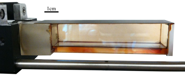
In this paper atom chips were placed outside of the vacuum envelope and were successfully used to trap laser cooled atoms. This was made possible by the combination of high power atom chips Squires et al. (2011) in close proximity to a thin monocrytalline silicon membrane which formed one wall of a custom vacuum chamber. The thin membrane enabled the trapping of laser-cooled atoms mm from the atom chip (see Fig. 1a). Tight atom-chip magnetic traps (i.e. trap frequencies kHz) were still possible, while external mounting of the chips enabled rapid and simple switching of atom chips without impacting the UHV environment. Production of a Bose-Einstein condensate (BEC) using ex vacuo atom chips, as well as trapping atoms in precision atom-chip magnetic potentials Stickney et al. (2014) were demonstrated. In comparison to other atom-chip systems Hänsel et al. (2001); Drndić et al. (1998); Aubin S. et al. (2006); Wang et al. (2005); Farkas et al. (2010), the atom chips were switched multiple times without breaking vacuum. Less than three hours was required to switch the atom chip and to achieve a magnetic trap with BEC compatible conditions. Additionally, the external mounting greatly simplified electrical connections and thermal management.
a.)
b.)
c.) 
II Construction
Two vacuum chamber designs are presented in this section. The two vacuum chambers were similar in design, but with some key differences such as silicon thickness (discussed in Sec. III). The chamber designs are presented to demonstrate the ability vary various construction details while maintaining the same functionality.
Both chambers used dual magneto-optical traps (MOTs) where a 2-D+ MOT Farkas et al. (2010) loaded a 3-D mirror MOT. A mirror MOT was used to allow the MOT to form in close proximity to the atom chip Fortagh et al. (1998), which assisted in the loading of the magnetic trap after laser cooling. The mirror was formed by depositing silver on the vacuum side of the silicon membrane. After laser cooling, the atoms were magnetically trapped using an ex vacuo atom chip mounted above the 3-D MOT chamber.
The chambers were constructed from silicon and borosilicate glass joined with a UHV-compatible epoxy (Epo-tek 353ND) Reichel et al. (2001). This method has been reliably used for constructing custom UHV chambers utilizing components that would be otherwise difficult to join using common glass blowing methods (e.g. double-sided anti-reflection coatings or dissimilar materials) or standard UHV components.
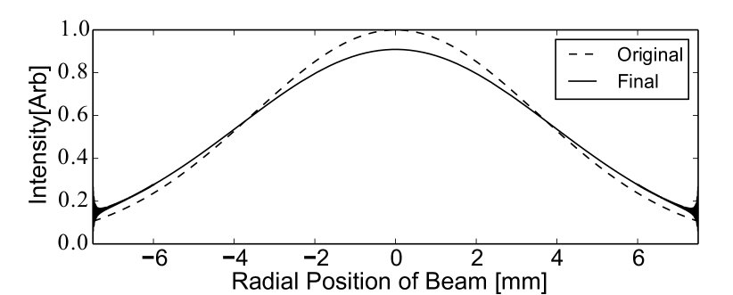
The first chamber was made using separate 2-D and 3-D MOT cells joined on opposite faces of a Conflat cube. This design was similar to the configuration in Ref. Squires (2008), except that one of the long sides of the 3-D MOT cell was sealed with a thin silicon membrane (see Fig. 1b). A ion pump and titanium sublimation pump were connected to one of the remaining ports. The exit aperture of the 2-D MOT was mm in diameter. The silicon membrane was 150 m thick and the deformation of the silicon could be seen when the chamber was evacuated. The calculated focal length of the deformed silicon was approximately cm. As shown in Fig. 2, the resulting intensity change was negligible within the MOT range. In this configuration the 3-D MOT loaded atoms.

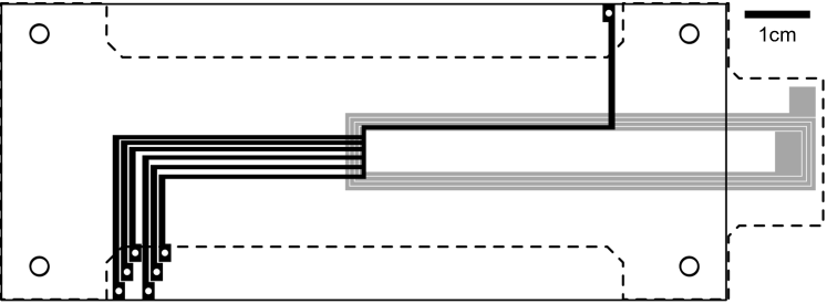
A magnetic trap was realized using this cell with multiple Z-wire iterations. Fig. 3a illustrates the final Z-wire configuration. During one of the atom chip changes, the silicon cracked along a crystal boundary. The cracked silicon was repaired with VacSeal, however the magnetic trap lifetime was degraded and a second chamber was built as a replacement.
a.)  b.)
b.) 
The second chamber was similar to the first chamber except for the following changes: 1) the entire chamber was epoxied together with a single 1.33” Conflat at the end of the 3-D MOT chamber; 2) the exit aperture of the 2-D MOT was 0.5 mm; 3) the silicon membrane was approximately 350 m thick; and 4) an intermediate chamber was epoxied between the 2-D and 3-D MOT chambers (see Fig. 1c). The intermediate chamber was approximately 25 mm square and filled with SAES ST 707 non-evaporable getter strips for passive pumping of residue gases released by the rubidium dispensers (SAES RB AMD). The exit hole of the intermediate chamber was 2 mm diameter. The double pinhole design was implemented to improve differential pumping between the chambers. There was minimal deflection of the thicker silicon membrane. The MOT number was atoms. Because of the similar MOT numbers with two different deformations, it did not appear that the small deformation of the silicon noticeably affected the MOT number or temperature.
The atom chip traces were laser etched and the chip outline was cut using a pulsed fiber laser milling system (Oxford Laser Systems) from commercially available direct bonded copper (DBC) substrates Squires et al. (2011). After laser etching, the resistance between traces was 5–50 . At this resistance, the chip wires were suitably isolated and the residual conductivity was due to copper slag from the laser etching process. A 1–30 s chemical etch in either HCl/H2O2 or cupric chlorate Cakir (2006) removed any residual copper. The final resistance between isolated copper areas was M.
Mounting and alignment holes were laser cut after laser etching the wire traces without removing the DBC substrate from the mill. These mounting holes were assumed to be aligned with the chip traces within the tolerance of the laser mill (m). The alignment holes were used to mount the atom chips relative to the vacuum chamber and allowed for precision alignment between the various atom chip layers (e.g. the U-wire chip and the BEC chips).
III Membrane Design and Testing
Trapping atoms as closely as possible to the atom chip conductors is critical for generating tight magnetic traps due to the nature of magnetic field gradients. As seen in Fig. 1a, the effective distance from an atom chip to the vacuum is , where is the thickness of the membrane and is the maximum displacement due to the bowing of the thin membrane. If the membrane is too thin, the distance to the atoms increases due to the bowing of the membrane (see Fig. 4). Conversely, if the membrane is thick, there is little bowing but the distance to the atoms increases due to the thickness of the membrane.
The maximum deflection at the center of a rectangular plate with fixed edges and uniformly applied pressure is
| (1) |
where is a numerical factor determined by the shape of the membrane, is the width of the cell, is the Young’s modulus of the material, is the pressure, and is the thickness of the membrane Hearn (1997). The optimal membrane thickness that minimizes the distance to the atoms is
| (2) |
In considering which materials to use, those with nearly matched coefficients of thermal expansion (CTE) were chosen to minimize the stress of the vacuum chamber during bakeout. Young’s modulus has little effect on optimal membrane thickness because of the scaling dependence. Thus, optimizing has minimal benefit. Silicon was used for the membrane and borosilicate glass for the rest of the chamber because of the nearly matched CTEs and polished silicon wafers are available in a wide variety of thicknesses.

| Material | CTE (K) | E (GPa) | Strength (MPa) |
|---|---|---|---|
| fused quartz | 0.55 | 72 | 48 |
| diamond (CVD) | 1.0 | 1,050 | 750 |
| borosilicate | 3.25 | 64 | 35–100 |
| Si | 3.55 | 112–165 | 7,000 |
| SiC | 4.0 | 405 | 3,440 |
| W | 4.5 | 400–410 | 1,510 |
| AlN | 4.8 | 308 | 400 |
| sapphire | 5.3 | 335 | 400 |
| WC | 6 | 450–650 | 345 |
| S.S. 302 | 15–18 | 200 | 520 |
The plausibility of using thin a silicon membrane as a vacuum wall was tested using a glass test cell with a mm opening that was sealed by a 150 m thick silicon membrane. This test membrane survived repeated pump/vent cycles and a vented cross-country laboratory move.
Separate burst testing was performed to determine the strength margin of the membrane and whether the silicon crystal orientation had any effect on the burst strength. A mm pocket was milled in an aluminum block and sanded flat. A variety of silicon membranes were epoxied to the aluminum block which was placed in a pressurized tube to simulate the evacuation of a vacuum chamber. The tube was over-pressurized to determine the strength of the membrane above atmospheric pressure. The majority of membranes ruptured at greater than 5 atmospheres of over-pressure with no apparent dependence on crystal orientation.
IV Results/Discussion
The implementation of laser cooling, magnetic trap, and RF evaporation were similar to other atom chip experiments Hänsel et al. (2001); Du et al. (2004); Farkas et al. (2010) with the exception of a few key experimental details highlighted here. Evanescently coupled polarization maintaining fiber splitters were used to divide the laser into multiple beams and to combine the cooling and repump lasers. A () splitter was used for the 2-D(3-D) MOT. The 2-D MOT used two mm elliptical beams and a 15 mm circular pusher beam; the 3-D MOT employed four 15 mm circular beams.
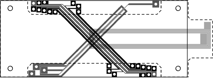
The MOT quadrupole field was generated with a U-wire atom chip Fortagh et al. (1998). Four loops on each side of the U-wire chip were connected by a soldered via (see Fig. 3). The U-wire chip was mounted on top of the BEC atom chip using common mounting holes. This allowed for a consistent alignment between the MOT and the other magnetic field generating chips and facilitated the rapid achievement of a magnetic trap after switching atom chips.
The MOT was loaded for s at 8.0 mm from the silicon surface. After loading, the atoms were cooled, compressed, and moved closer to the membrane within 80 ms during the compressed MOT (CMOT) stage. The magnetic fields were then ramped off for molasses cooling. The U-wire and bias magnetic field coils were controllably ramped off in 1 ms to ensure the position of the CMOT did not significantly move prior to molasses cooling. The lasers were then further detuned for 6 ms of molasses cooling. The cooling laser was then shuttered. The atoms were then optically pumped into the state. After optical pumping there were approximately atoms at 15 K.
These atoms were initially captured in a Z-wire magnetic trap using the largest Z (see Fig. 3a) with 47.9 A in the Z-wire and G, which formed the initial trap at 4.6 mm from the silicon surface. The largest Z was used for the initial trap because the depth of the trap depends on the trap height to Z-wire width ratio, i.e., beyond a maximum distance from the wires there is no longer a trap. For two parallel wires with current in the same direction, no trap was formed when the height was greater than width.
After the initial trap, the cloud was compressed by increasing the bias field and trapping in successively smaller Z-wires. The Z-wire electrical configuration was changed by linearly switching the current between adjacent Z-wire leads to maintain a constant current in common lead of the Z-wire. The contribution to the By field from the Z-wire depended on the width of the Z-wire. The By bias field was adjusted during the compression to maintain a constant bottom magnetic field during the Z-wire lead switching. The final trap used the next to smallest Z-wire with external bias fields G and A for calculated trap frequencies of Hz and a trap at 1.25 mm from the silicon surface. The atoms were not ramped closer at this stage because of surface losses due to the proximity of silicon membrane.
The atoms were then cooled via RF evaporation. As the cloud cooled, it became smaller which allowed the trap to be compressed and ramped closer to the chip without additional surface losses. The RF sweep and compression sweeps followed a functional form. The first sweep ramped the RF frequency from 50 MHz – 6 MHz and the Bx field was ramped from 35 – 75 G with in 6 s. The final calculated trap parameters were Hz at 0.5 mm from the silicon surface at 39 A and G. After the first RF sweep the trap was not compressed further.
A second RF sweep ramped the RF frequency from 6 MHz–4.9 MHz in 1 s with an exponent factor . The BEC transition was detected by a sharp change in the effective area of the atom cloud Lye et al. (2002). The transition temperature was 150 nK with atoms.
After first achieving BEC in the multi-Z compression trap, the multi-Z atom chip was replaced by the the atom chip shown in Fig. 3b. The central wires on each side of the atom chip were connected in series. The field of those wires plus an additional bias field were used to create the magnetic trap. Unlike the Z-wire design, there was no height:width ratio that limited the maximum trapping distance. As configured here, the cross-wire trap had a non-zero magnetic field bottom and was used for evaporative cooling and BEC production. The function of the other wires is described in Ref. Stickney et al. (2014).
The new atom chip was installed in approximately two hours. Most of that time involved careful routing of the 26 electrical connections to the chip (see Fig. 3b). The new atom chip was attached to the chamber using the same mounting holes as the Z-wire atom chip.
A MOT with nominal number and temperature was obtained within minutes of installing the new atom chip assembly. A magnetic trap was achieved in less than 30 minutes after installation. The new atom chip experiments are described in Ref. Stickney et al. (2014). These experiments do not require BEC but rather atoms evaporatively cooled to K. Evaporation using the new atom chip was as efficient as evaporation in the Z-wire atom chip.
Since the first install, several wiring changes have been made with the new atom chip configuration. These changes have required the atom chip to be removed and reinstalled. Additionally, a BEC has been made with the cross-wire trap. Each time the atom chip has been installed, nominal operating conditions have been reestablished in less than 30 minutes with little optimization.
This paper has described the design and building of an atom chip system where ex vacuo atom chips are placed next to a thin membrane forming one wall of the vacuum system. The thin membrane coupled with a high power DBC atom chip enables tight magnetic traps compatible with BEC production. This setup greatly simplifies the rapid replacement of atom chips. Magnetic traps and BECs have been produced with two different atom chip configurations with minimal downtime between experiments.
V Acknowledgements
We gratefully acknowledge Benjamin Stuhl and Rudolph Kohn for their careful reading of this manuscript.
References
- Reichel (2002) J. Reichel, Appl. Phys. B 74, 469 (2002).
- Du et al. (2004) S. Du, M. B. Squires, Y. Imai, L. Czaia, R. A. Saravanan, V. Bright, J. Reichel, T. W. Hänsch, and D. Z. Anderson, Phys. Rev. A 70, 053606 (2004).
- Aubin S. et al. (2006) Aubin S., Myrskog S., Extavour M. H. T., LeBlanc L. J., McKay D., Stummer A., and Thywissen J. H., Nat Phys 2, 384–387 (2006), 10.1038/nphys309.
- Schumm et al. (2005) T. Schumm, S. Hofferberth, L. M. Andersson, S. Wildermuth, S. Groth, I. Bar-Joseph, J. Schmiedmayer, and P. Kruger, Nat Phys 1, 57 (2005).
- Günther et al. (2005) A. Günther, M. Kemmler, S. Kraft, C. J. Vale, C. Zimmermann, and J. Fortágh, Phys. Rev. A 71, 063619 (2005).
- Horikoshi and Nakagawa (2006) M. Horikoshi and K. Nakagawa, Applied Physics B: Lasers and Optics 82, 363 (2006).
- Squires et al. (2011) M. B. Squires, J. A. Stickney, E. J. Carlson, P. M. Baker, W. R. Buchwald, S. Wentzell, and S. M. Miller, Review of Scientific Instruments 82, 023101 (2011).
- Stickney et al. (2014) J. A. Stickney, B. Kasch, E. Imhof, B. R. Kroese, J. A. R. Crow, S. E. Olson, and M. B. Squires, ArXiv e-prints (2014), arXiv:1407.6398 [physics.atom-ph] .
- Hänsel et al. (2001) W. Hänsel, P. Hommelhoff, J. Reichel, and T. W. Hänsch, Nature 413, 498 (2001).
- Drndić et al. (1998) M. Drndić, K. S. Johnson, J. H. Thywissen, M. Prentiss, and R. M. Westervelt, Applied Physics Letters 72, 2906 (1998).
- Wang et al. (2005) Y.-J. Wang, D. Z. Anderson, V. M. Bright, E. A. Cornell, Q. Diot, T. Kishimoto, M. Prentiss, R. A. Saravanan, S. R. Segal, and S. Wu, Phys. Rev. Lett. 94, 090405 (2005).
- Farkas et al. (2010) D. M. Farkas, K. M. Hudek, E. A. Salim, S. R. Segal, M. B. Squires, and D. Z. Anderson, Applied Physics Letters 96, 093102 (2010).
- Fortagh et al. (1998) J. Fortagh, A. Grossmann, C. Zimmermann, and T. W. Hänsch, Phys. Rev. Lett. 81, 5310 (1998).
- Reichel et al. (2001) J. Reichel, W. Hänsel, P. Hommelhoff, and T. W. Hänsch, Applied Physics B: Lasers and Optics 72, 81 (2001).
- Squires (2008) M. B. Squires, High repetition rate Bose-Einstein condensate production in a compact, transportable vacuum system, Ph.D. thesis, University of Colorado at Boulder (2008).
- Cakir (2006) O. Cakir, Journal of Materials Processing Technology 175, 63 (2006), achievements in Mechanical & Materials Engineering.
- Hearn (1997) E. Hearn, Mechanics of Materials 2, 3rd Ed (Butterworth-Heinemann, 1997) Chap. 7.
- Lye et al. (2002) J. E. Lye, C. S. Fletcher, U. Kallmann, H.-A. Bachor, and J. D. Close, Journal of Optics B: Quantum and Semiclassical Optics 4, 57 (2002).