Sub-THz thermally activated-electrical conductivity of CdS thin films.
Abstract
The electrical conductivity of a CdS thin film, controlled by grain structures is essential to enhance its photoconductivity to be able to be fit as a window material in CdS/CdTe heterojunction solar cell. In order to characterize a thin film, electromagnetically, we employed an open cavity resonator with a sub-millimeter VNA (Vector Network Analyzer). Our technique is capable of measuring complex dielectric permittivity, , of a photovoltaic film as thin as 0.1 m. We measured the real part of the complex dielectric permittivity, , and electrical conductivity, (derived from the imaginary part, ), of unannealed and annealed CdS films with thicknesses 0.15 m on 3 mm thick-borosillicate glass substrates, at room temperature. We obtain the (thermally activated) electrical conductivity between 100 and 312 GHz, which is less in annealed samples than in unannealed one by 2 orders of magnitude. Contrary to our expectations, the carrier concentrations extracted from these data by fitting a Drude model, are 1016 cm-3 (unannealed) and 1014 cm-3 (annealed). We investigate the connection between grain size and carrier concentration.
Cadmium sulphide (CdS) is an integral component of CdTe/CdS heterostructured-thin solar cell where it is used as a window material for its better photoconductivity, optolelectronic properties, and flexibilty.(Chu et al., 1991; Aramoto et al., 1997; Tsuji et al., 2000) Its photoconductivity sensitivity depends on its electronic properties. CdS is usually layered with cadmium telluride (CdTe) to make efficient solar cells.(Moutinho et al., 2006; Townsend, 2001) Cadmium sulphide (CdS) contains many intrinsic defect-states which affect its electronic conductivity profile. The grain structure can also plays a role. The microstructures of polycrystalline materials are composed of different oriented-grains.(Bube, 1992, 1960) The grain boundaries are characterized by a potential barriers. The photoexcitation can impact transport through these grain boundaries by various mechanisms. The electrical conductivity is the key property in all these phenomena. This photovoltaic material can be grown with many different techniques, and dielectric properties are growth-technique dependent.
The annealing-effects (in vacuum and under argon atmosphere) on the electrical and optical conductivity of CdS (deposited by chemical bath deposition method) have been studied in the temperature range 200-400 K.(Oumous and Hadiri, 2001) In the article by Oumous and Hadiri (2001), for temperatures 300 K, the conduction is explained by the traps at the grain boundaries for grains partially depleted. On the other hand, for temperatures 300 K, the conduction results from a hopping due to localized states.
In order to evaluate the quality of materials used in CdS/CdTe photovoltaic heterojunctions, the complex dielectric properties of polycrystalline CdS, formed into a thin film by sputter-deposition onto Silicon (Si) wafers, were investigated by in situ spectroscopic ellipsometry.(Li et al., 2010) The authors focused on understanding the excited carriers by fitting their data to carrier scattering model. This is in optical frequency range (0.75 to 6.5 eV).
Kazmerski et al. (1972a) illustrated the relationship between the electrical properties, i.e. conductivity and mobility, and the defects produced by grain boundaries and surfaces. These experiments were done in slowly deposited polycrystalline CdS thin films, and at temperatures as 1300C and 1800C. The mobility is found to be strongly dependent of grain size, and function of substrate temperature as well. They found a critical point that the grain boundary potential varies with deposition rate. In a second paper(Kazmerski et al., 1972b) they investigated how the stacking-faults along with grain-boundary affecting surface scattering impact greatly conductivity.
The electrical conductivity and mobility of polycrystalline CdS thin films (prepared by spray pyrolysis) at dark and under illumination were performed to correlate with thicknesses.(El Akkad and Ashour, 2009) Point defects play a vital role in this case.
A photoluminescence technique reveals the inhomogeneous distribution of localized defect states of polycrystalline semiconductors (for examples, CdS and CdTe).(Albert et al., 2013) These defects are responsible for long-range photoconductivity through multiple grain boundaries.
Bube (1968) explained that polycrystalline CdS can be treated as a series connection between grain interior and boundary, and illustrated to be inhomogeneous electronic conductivity. In Bube’s model, the grain interior and boundary contain high and low conductivity respectively. Even though carrier concentration and mobility are both competitive mechanisms, still it is not resolved which one becomes more dominant and under what condition.
The electrical conductivity of thin-film semi-conductors is hard to measure in the far-infrared or sub-millimeter regime. Sources, both pulsed (laser-based) or steady state (either laser photo-mixing or high harmonic generation of microwaves) are relatively weak, and the film thicknesses of interest in photovoltaics are much less than the wavelength of the probe beam. Nevertheless, we want to understand the conductivity behavior of CdS films in the sub-millimeter regime since this is where electronic and optical properties strongly overlap.
In this paper, we measure THz conductivity at room temperature. We use perturbation of an open hemispherical cavity resonator(Rahman et al., 2013) to probe complex dielectric constants of CdS thin films, unannealed and annealed. This method is also able to observe laser-induced photoexcitation measurements.(Rahman et al., 2014) Even though in this sub-THz range the phonon-mediated mechanisms are predominant,(Zallen, 2005) we confirm the presence of THz electrical conductivity in CdS thin films.
The CdS films were thermally evaporated in a vacuum chamber. CdS pieces were placed in a 6 mm quartz crucible that was heated by a tungsten filament. The vacuum was approximately 3 X 10⁻⁶ torr. The substrate temperature was approximately 1500C.
We measure DC resistivity of CdS thin films with a van der Pau type device where a Lakeshore 7506 Hall system with an excitation current of 10 nA is implemented for such DC measurements.
Rahman et al. (2013, 2014) describe the open cavity method for measuring complex dielectric properties of thin films in detail. In this experiment, we repeated the whole process (of putting the sample into the cavity and taking out) for five times to estimate the measurement uncertainy. The pointwise standard deviation is calculated to be less than 1 of the measured spectra. The dark and room light measurements of dielectric constant () and conductivity () for both (unannealed and annealed) CdS films give the identical values. Moreover, between 100-180 GHz, the conductivity remains constant in frequency. Due to absence of -dependence, this does not represent any phonon vibrations or damping. Therefore, at room temperature, this is an indication of thermally-activated electronic conductivity.
The classical Drude model for frequency-dependent (real part of) conductivity is expressed by
| (1) |
where, is the complex conductivity, is the dc conductivity and is the average collision time of electrons. It is a macroscopic parameter containing both trap-capture time and also release-time.
The DC conductivity is defined by
| (2) |
With is the constant electron-concentration (holes are ignored because of low-mobility and the films are typically n-type), is the electronic charge and is the constant electron mobility. The relation between the frequency-dependent electron mobility, and effective electron mass is =(), where, , defined as carrier(electron) damping rate. Now, the dispersion in , , and in , , make them harder to calculate. To do that, we have to find the frequency-dependence in and .
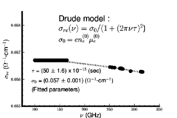
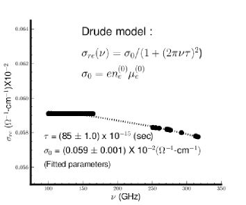
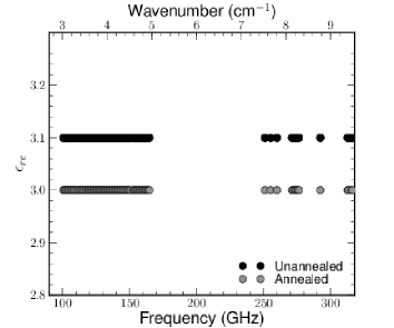
Figure 1, 2 and 3, shows that the experimental data and the model described by Eq.(1). For unannealed CdS films, the fit parameters, = (50.0 1.6) x 10-15 sec., and = (0.057 0.001) cm-1; for annealed one, = (85.0 1.0) x 10-15 sec., and = (0.059 0.001) X 10-2 cm-1 are extracted from fitted-model.
(∗ indicates femtosecond: 1 fs = 10-15 sec)
| CdS-samples | Collision time | DC conductivity | Carrier concentration |
| n | |||
| (fs)∗ | ( cm-1) | (cm-3) | |
| Unannealed | (50.0 1.6) | (0.057 0.001) | (3.65 0.01) X 1016 |
| Annealed | (85.0 1.0) | (0.00059 0.00001) | (3.70 0.01) X 1014 |
The upper limit of electron mobility, 10 cm2V-1sec-1 at room temperature is reported.(Le Comber and Spear, 1970) The formula is used for calculating , is given as , based on the models.(Cohen, 1970; Mott, 1969) Here, is interatomic seperation and is the frequency of an electron, typically 1015 sec-1. Using Eq.(1), the carrier concentrations, n, in unannealed and annealed samples are (3.65 0.01) x 1016 cm-3 and (3.70 0.01) x 1014 cm-3, respectively, at room temperature. Therefore, unannealed CdS contains 102 more carriers (per cm3) than that of annealed one.
Annealing makes the grain size larger and the depletion zone is wider including grain boundaries. This depletion layer contains negligible carrier conentrations, and due to higher potential barrier, the conductivity of electrons decrease at room temperature (without any external excitations such as lasers).Li et al. (2012) mentioned that CdS thin films or nano belts are typically n-type due to sulfur vacancies on the surfaces. These are apparently active sites where the adsorptions of oxygen/water occur. Two depletion layers near both surfaces of nanobelts are created because of capturing intrinsic free electrons. This process of trapping carriers can extend the width of the depletion layers during annealing of CdS thin films. The conductivity is extremely low due to lack of carriers which is also indicated by high resistivity (by DC conductivity measurements). On the other hand, there is no clear demarcation between grain interior and boundary in an unannealed one. Therefore, the space-charge region where the depletion region resides, is small and results in a higher carrier concentration (than that of annealed sample). This also enhances electrical conductivity due to low potential barrier. In higher frequency regions (250 - 320 GHz), the annealed sample shows slower decaying- electrical conductivity even though the average collision time is faster than that of the unannealed one; this is because it contains much lower carrier concentrations due to backscattering or localizations.
This work was supported by the US Department of Energy (Basic Energy Science) under grant DE-FG02-09ER16018. The authors would like to thank Dr. Joe Beach, at Colorado School of Mines, for preparing these CdS thin films by thermally sublimation method. We are very thankful to Dr. Tim R. Ohno for his DC conductivity measurements on these samples and invaluable discussions on the grain size and electrical conductivity of CdS/CdTe type materials.
References
- Chu et al. (1991) T. L. Chu, S. S. Chu, C. Ferekides, Q. C. Wu, and J. Britt, J. Appl. Phys. 70, 7608 (1991).
- Aramoto et al. (1997) T. Aramoto, S. Kumazawa, H. Higuchi, T. Arita, S. Shibutani, T. Nishio, J. Nakajima, M. Tsuji, A. Hanafusa, T. Hibino, et al., Jpn. J. Appl. Phys. 36, 6304 (1997).
- Tsuji et al. (2000) M. Tsuji, A. Tetsuya, H. Taeshi, and O. Kuniyoushi, Journal of Crystal Growth 214/215, 1142 (2000).
- Moutinho et al. (2006) H. R. Moutinho, R. G. Dhere, C. S. Jiang, T. Gessert, A. Duda, M. Young, W. K. Metzger, and M. M. Al-Jassim, in IEEE 4th World Conference on Photovoltaic Energy Conversion (WCPEC-4), Waikoloa, Hawaii, USA, May 7-12, 2006, NREL/CP-520-39802 (IEEE, 2006).
- Townsend (2001) S. W. Townsend, Electrical and Optical Properties of Bias Stressed Cadmium Telluride Solar Cells, Ph.D. thesis, Colorado School of Mines (2001).
- Bube (1992) R. H. Bube, Photoelectronic Properties of Semiconductors (Cambridge University Press, 1992).
- Bube (1960) R. H. Bube, Photoconductivity of Soilds (New York : Wiley, 1960).
- Oumous and Hadiri (2001) H. Oumous and H. Hadiri, Thin Solid Films 386, 87 (2001).
- Li et al. (2010) J. Li, J. Chen, and R. W. Collins, Appl. Phys. Lett. 97, 181909 (2010).
- Kazmerski et al. (1972a) L. L. Kazmerski, W. B. Berry, and C. W. Allen, J. Appl. Phys. 43, 3515 (1972a).
- Kazmerski et al. (1972b) L. L. Kazmerski, W. B. Berry, and C. W. Allen, J. Appl. Phys. 43, 3521 (1972b).
- El Akkad and Ashour (2009) F. El Akkad and H. Ashour, J. Appl. Phys. 105, 093113 (2009).
- Albert et al. (2013) K. Albert, B. Fluegel, H. Moutinho, R. G. Dhere, J. V. Li, and A. Mascarenhas, Nature Communications 4, 1 (2013).
- Bube (1968) R. H. Bube, Appl. Phys. Lett. 13, 136 (1968).
- Rahman et al. (2013) R. Rahman, P. C. Taylor, and J. A. Scales, Review of Scientific Instruments 84, 083901 (2013).
- Rahman et al. (2014) R. Rahman, T. R. Ohno, P. C. Taylor, and J. A. Scales, Appl. Phys. Lett. 104 (2014).
- Zallen (2005) R. Zallen, The Physics of Amorphous Solids (Wiley-VCH Verlag GmbH & Co. KGaA, 2005).
- Le Comber and Spear (1970) G. P. Le Comber and W. E. Spear, Phys. Rev. Lett. 25, 509 (1970).
- Cohen (1970) M. H. Cohen, Journal of Non-crystalline Solids 4, 391 (1970).
- Mott (1969) N. F. Mott, Phil. Mag. 19, 835 (1969).
- Li et al. (2012) M. Li, B. Wu, B. I. M. Utama, Q. Xing, T. C. Sum, and X. Zhang, Appl. Phys. Lett. 101, 091104 (2012).