Resonant enhancement in nanostructured thermoelectric performance via electronic thermal conductivity engineering
Abstract
The use of an asymmetric broadening in the transport distribution, a characteristic of resonant structures, is proposed as a route to engineer a decrease in electronic thermal conductivity thereby enhancing the electronic figure of merit in nanostructured thermoelectrics. Using toy models, we first demonstrate that a decrease in thermal conductivity resulting from such an asymmetric broadening may indeed lead to an electronic figure of merit well in excess of in an idealized situation and in excess of in a realistic situation. We then substantiate with realistic resonant structures designed using graphene nano-ribbons by employing a tight binding framework with edge correction that match density functional theory calculations under the local density approximation. The calculated figure of merit exceeding in such realistic structures further reinforces the concept and sets a promising direction to use nano-ribbon structures to engineer a favorable decrease in the electronic thermal conductivity.
I Introduction
Low-dimensional systems Hicks and Dresselhaus (1993a, b); Dresselhaus et al. (2007); Snider and Toberer (2008); Mahan and Sofo (1996); Heremans et al. (2008); Nakpathomkun et al. (2010) and nanostructures Poudel et al. (2008); Agarwal and Muralidharan (2014); Dresselhaus et al. (2007) are envisioned as promising directions en route to the enhancement of the thermoelectric figure of merit. The thermoelectric figure of merit, , is defined as
where is the Seebeck coefficient, is the electronic conductivity is the electronic thermal conductivity and is the lattice thermal conductivity. The term , appearing in the numerator is referred to as the power factor, and it relates to the actual electrical power that can be drawn by the load Nemir and Beck (2010). While much of the work on enhancement has focused on engineering a decrease in the lattice thermal conductivity Dresselhaus et al. (2007); Poudel et al. (2008); Gunst et al. (2011); Mazzamuto et al. (2011); Sevinçli and Cuniberti (2010); Feng and Ruan (2016); Xie et al. (2016), electronic engineering that aims to enhance the electronic figure of merit , is somewhat a less explored direction Shakouri (2011). In this context, the traditional direction followed is that of increasing the power factor via electron filtering Faleev and Léonard (2008); Shakouri (2011) in low-dimensional structures Hicks and Dresselhaus (1993a, b); Nakpathomkun et al. (2010); Shakouri (2011).
In a seminal work Mahan and Sofo (1996), Mahan and Sofo pointed out that an infinite value of may be asymptotically achieved in the limiting case when the un-broadened DOS and hence the transport distribution Muralidharan and Grifoni (2012) or equivalently, the transmission function tends to a delta distribution. This is typically achieved in a quantum dot system in the limit of vanishing coupling to the contacts. Apart from the thermodynamic interpretation of achieving the Carnot efficiency Humphrey and Linke (2005); Esposito et al. (2009a, b, 2010); Muralidharan and Grifoni (2012), the infinite is attributed to the vanishingly small electronic thermal conductivity Mahan and Sofo (1996); Muralidharan and Grifoni (2012). This is simply because the delta transport distribution produces a zero variance in energy, leading to a zero electronic thermal conductivity. Thus a resonant enhancement in the electronic DOS is often a sought after route that combines electron filtering with electronic thermal conductivity engineering Heremans et al. (2008); Hicks and Dresselhaus (1993a, b); Mahan and Sofo (1996), and this will be the primary focus of the current paper.
There has hence been significant interest in molecular Reddy et al. (2007), quantum dot Sothmann et al. (2015); Muralidharan and Grifoni (2012), super-lattice thermoelectric generators Jordan et al. (2013); Choi and Jordan (2015); Agarwal and Muralidharan (2014), and also other systems which feature a resonant distortion in the DOS Heremans et al. (2008), all of which aim to emulate a delta like transmission peak via sharp resonant levels. While the engineering of lattice thermal conductivity concerns the design of interfaces to increase phonon scattering, the aforementioned ideas lay the basic foundations to work with the electronic thermal conductivity by tailoring the electronic DOS.
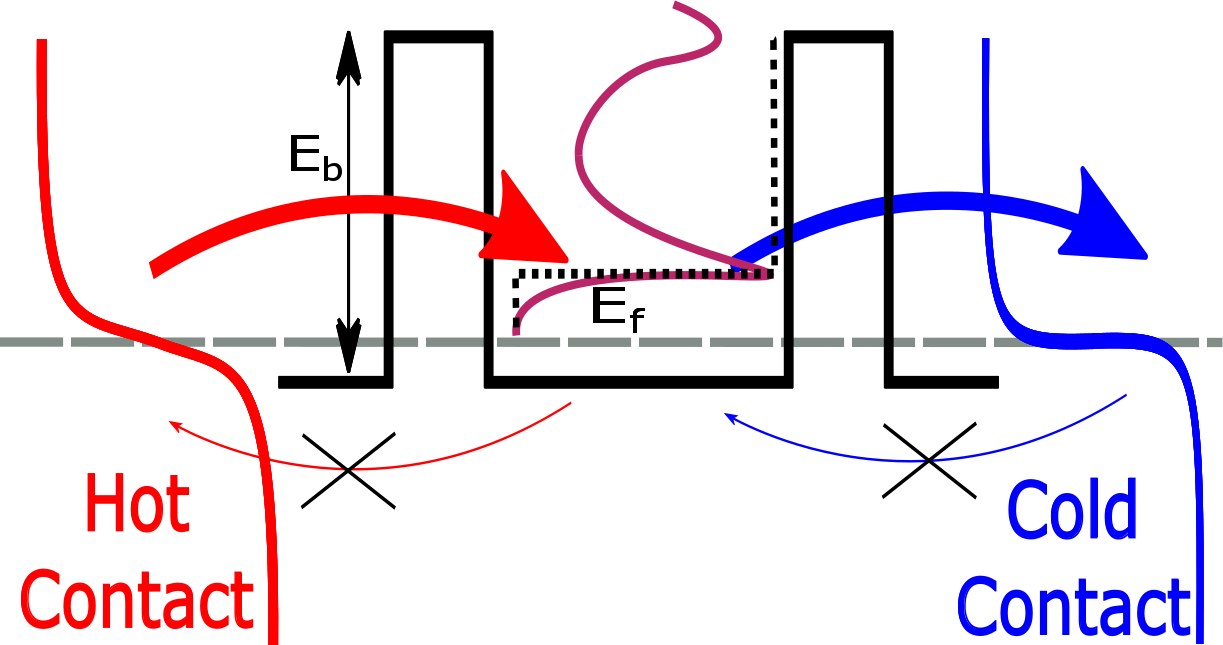
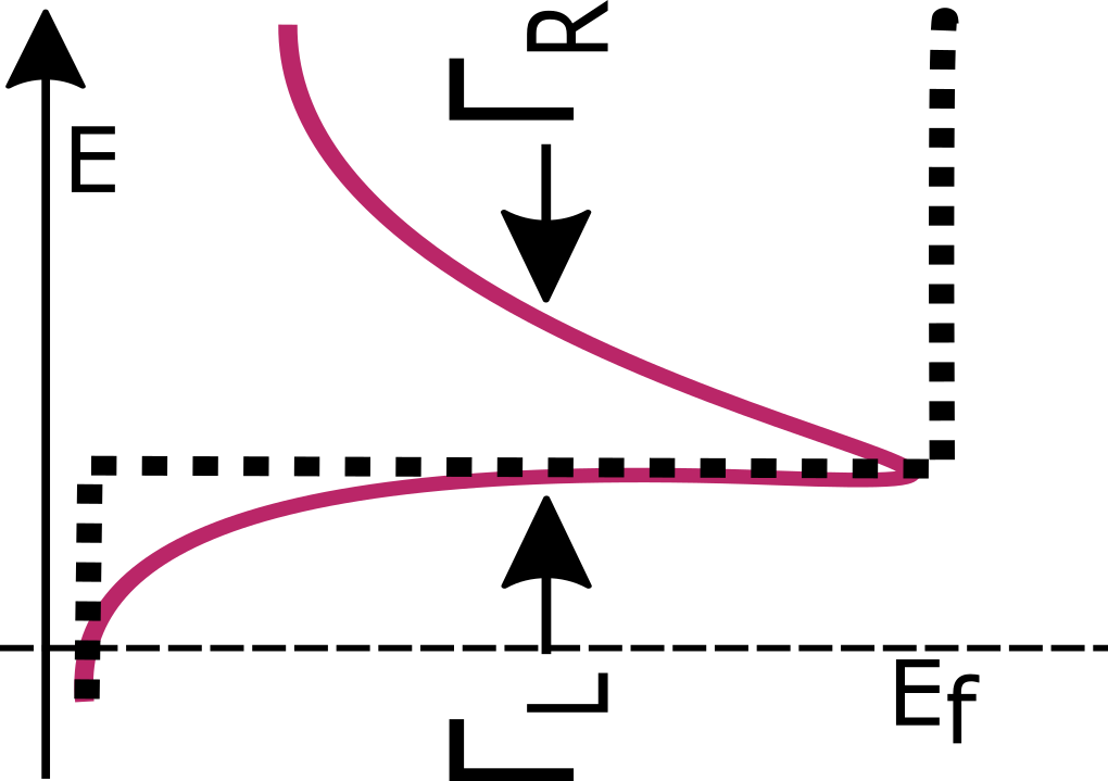
Quantum broadening of energy levels is, however, an inevitable by-product of electronic transport Lundstrom and Datta (2012); Muralidharan and Grifoni (2012), which arises due to coupling with the contacts or electrodes. As a result of broadening, deteriorates drastically as the broadening becomes significant. A schematic depicting this aspect is shown in Fig. 1(a), and (b), where the broadening of resonant levels in a quantum well is schematically sketched. It must be noted that, traditionally, perfect electron filtering involves a step like transmission function as depicted in Fig. 1(b), where current flow along only one direction occurs when the Fermi level lies below the band edge. It is hence critical that the broadening function be manipulated, so as to engineer a favorable trade-off between electron filtering and thermal conductivity decrease, should we decide to think along the direction that was proposed in Ref. [5]. In this paper, we propose one such method to tailor the broadening function so as to engineer a decrease in the electronic thermal conductivity and substantiate it with resonant tunnelling devices using graphene nano-ribbons.
The schematic of a resonant tunnelling device is shown in Fig. 1, where the absence of states in the channel at energies below the Fermi level in the transport window leads to no net flow of electrons between cold and hot contacts. Furthermore, a characteristic of such a double barrier structure is an asymmetric broadening of the transmission peaks. This is caused due to an inherent asymmetry between the low lying and higher energy states resulting from the band edge in the contact region Overhauser (1989). Our first task is to show that asymmetrically broadened peaks may result in a of 1000 as compared to the step transmission function in typical quantum well structures.
II Formulation
In order to formalize the concepts stated above, we employ the transmission formalism in the linear response regime Lundstrom and Datta (2012) to evaluate the transport coefficients from the quantum mechanical transmission function:
| (1) |
| (2) |
| (3) |
where
| (4) |
with being the electronic charge, being the Planck’s constant, being the Boltzmann constant with being the temperature of the cold contact, being the Fermi level. Here, is the energy resolved transmission function and is the equilibrium Fermi-Dirac distribution function given by where .
For multi-moded structures, we calculate the effective transmission with transport along the direction and summing over the transverse modes evaluated by solving the transverse eigenvalue problem Agarwal and Muralidharan (2014) . For example, in the pure three dimensional (3-D) case Datta (2005), this can be written as , where is the two dimensional density of states and is given by .
III Results
III.1 Toy model: Thermal conductivity engineering
’
’
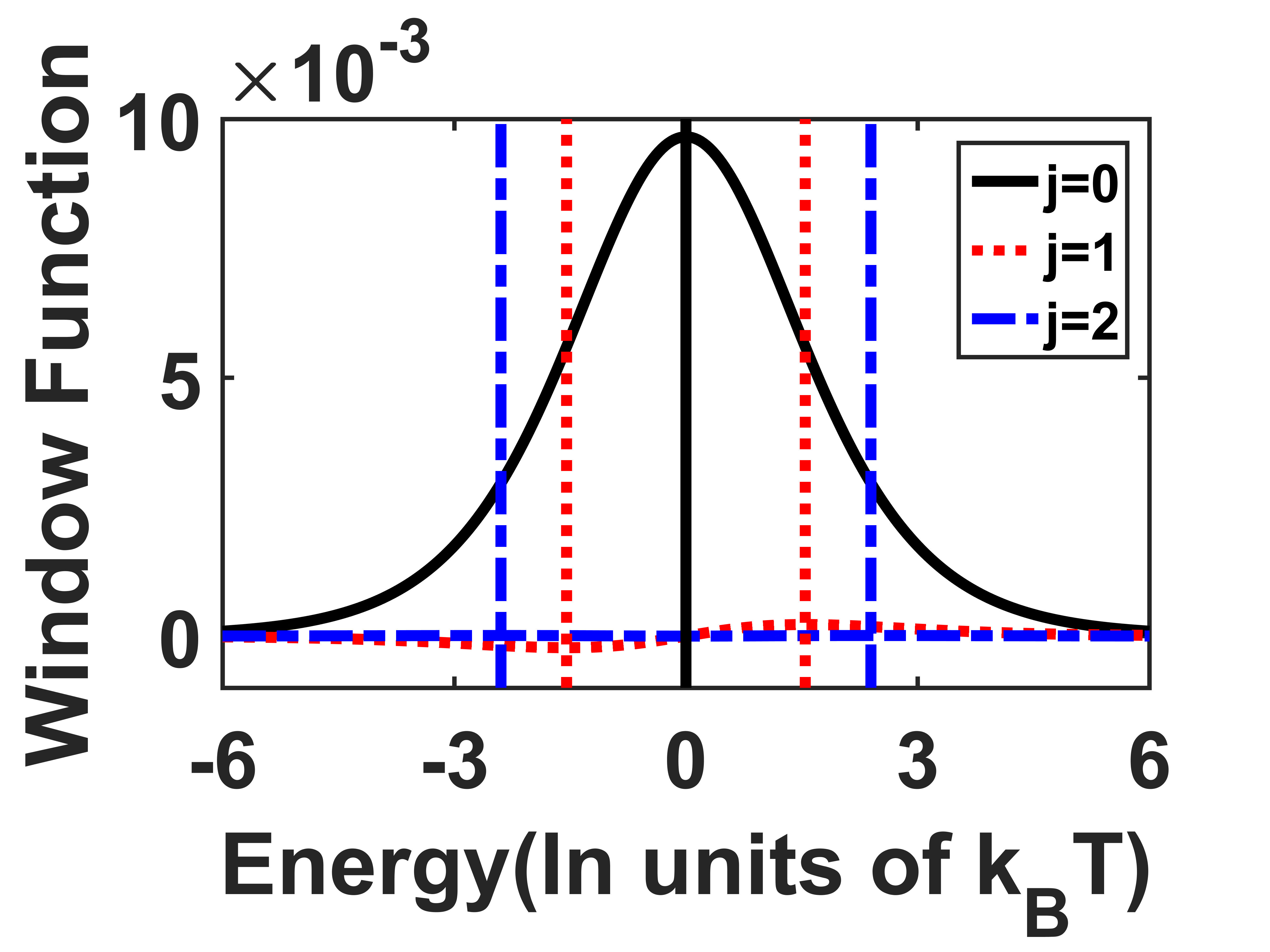
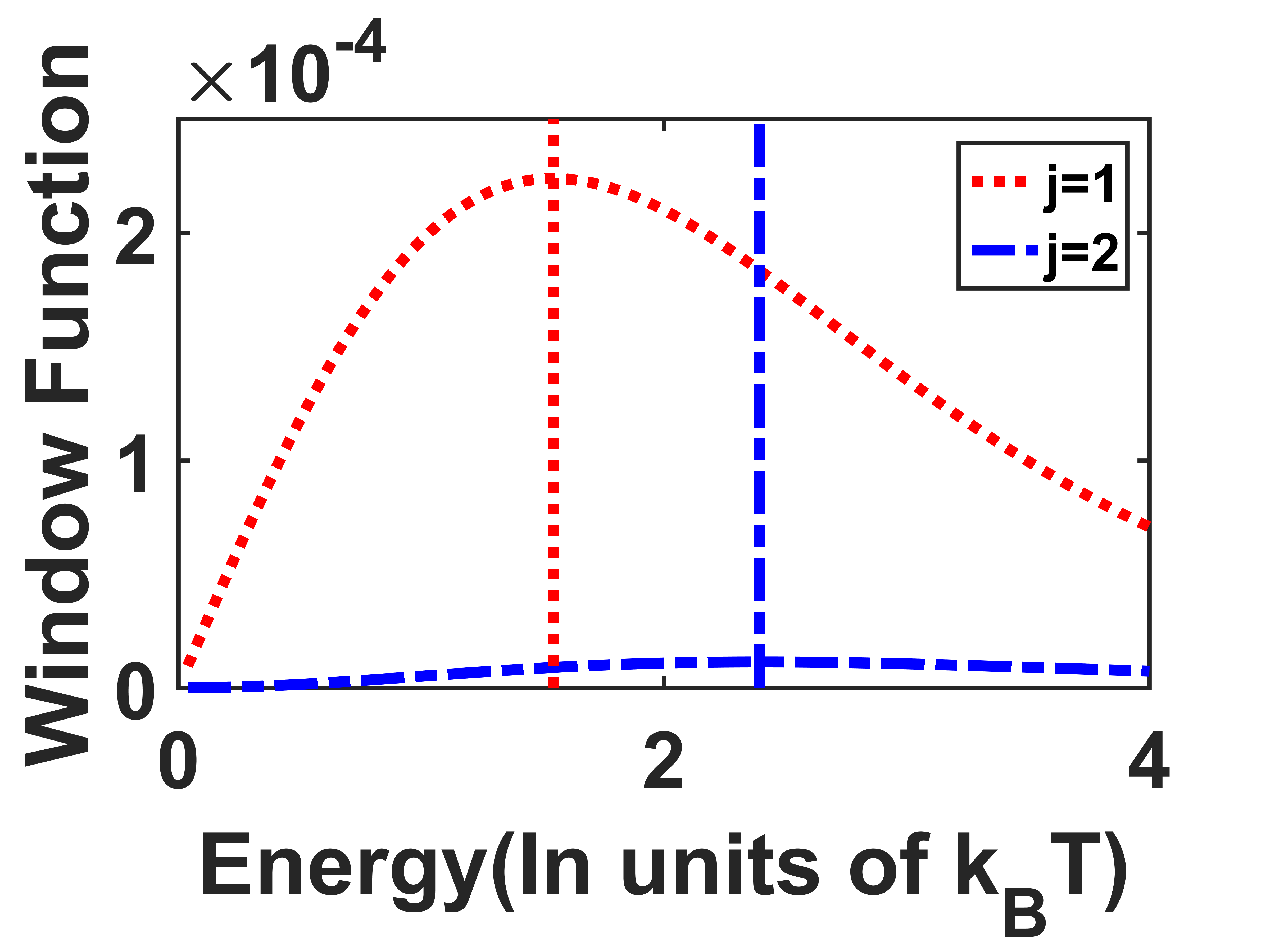
The rudiments of engineering the electronic thermal conductivity follow from simple arguments based on the energy distribution of the transport coefficients. The electrical conductivity at a given energy is directly dependent on the difference in the occupation factor of the electrons in the contacts, which at small temperatures maximizes at the Fermi level and dies down sharply upon detuning from it as seen from Fig. 2(a). On the other hand, the electronic thermal conductivity, , has a strong dependence on how energetically farther away the electronic energy is from the Fermi level . Due to the term in (4) being a product of a decreasing function and an increasing function , its resulting peak is further away from as seen in Fig. 2(b). Same is the case with the Seebeck coefficient . However since the increasing term is linear, the peak in this case is much closer to as seen in Fig. 2(b). This linear dependence also makes the function odd around thus providing a constraint that the electronic transmission should be on one side of . If the transmission is such that only electrons very close to participate in transport, it will result in a drastic decrease in with a marginal decrease in the and .
Let us consider an asymmetric transmission function based on the Lorentzian density of states Datta (2005) given by:
| (5) |
where represent heuristically, the broadening above (below) the central energy . Observe that this transmission function for certain values of only allows transmission of few states near its peak while keeping the transmission function one sided.
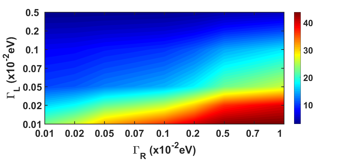
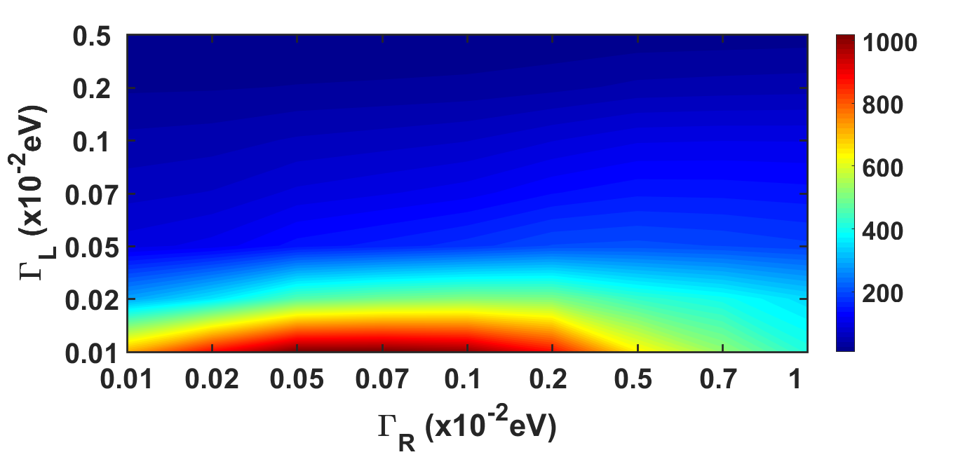
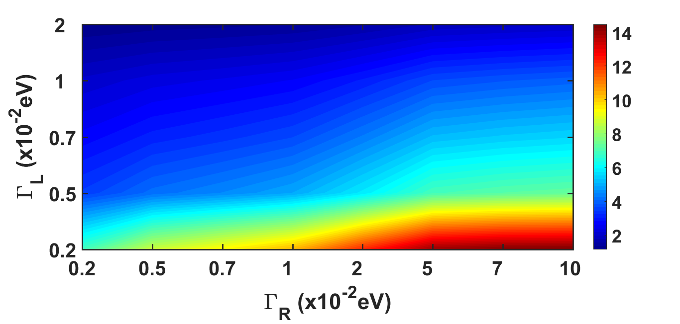
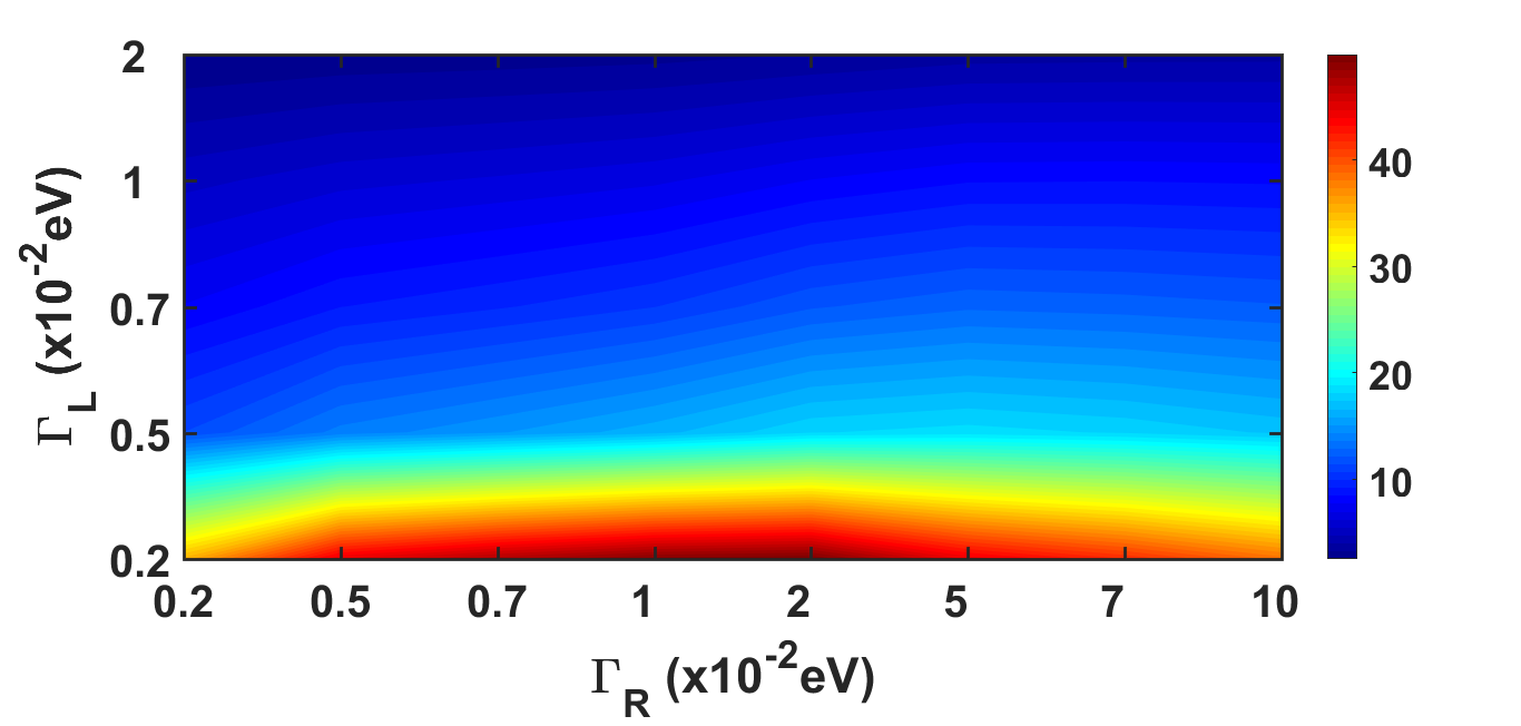
We plot in Fig. 3(a),(c) and Fig. 3(b),(d), the variation of in three dimensional (3-D) structures and one dimensional (1-D) structures respectively, as a function of and . For a 3-D structure, we have integrated over the transverse modes, and the 1-D device represents a purely one dimensional transmission. We observe from Fig. 3(a),(c) and Fig. 3(b),(d), that when , the electronic figure of merit is larger in comparison to when for both 1-D and 3-D structures. Also, as discussed earlier, an increase in the sharpness of the cut-off at the energy center via a decrease in , results in an increase in the , due to a suppression of reverse electronic flow below the Fermi level. It is also noted by comparing Fig. 3(a),(c) and Fig. 3(b),(d), that a 1-D structure gives rise to a much better performance in .
The transmission function proposed here decreases both the electrical conductivity and the electronic thermal conductivity. But due to the special nature of the window functions stated above, the percentage decrease in the three quantities is not the same. The percentage decrease in the Seebeck coefficient is much smaller than the percentage decrease in the electronic thermal conductivity and since we are interested in the ratio of these quantities, this disproportional change in the quantities of the numerator and the denominator of results in its increase. On comparing Fig. 3(b),(d), we note that while an ultra high may be achieved in 1-D structures with very small ambient broadening, a realistic broadening profile may also result in favorable figures of merit.
We will now take a closer look into the implications of the above on the thermoelectric performance.
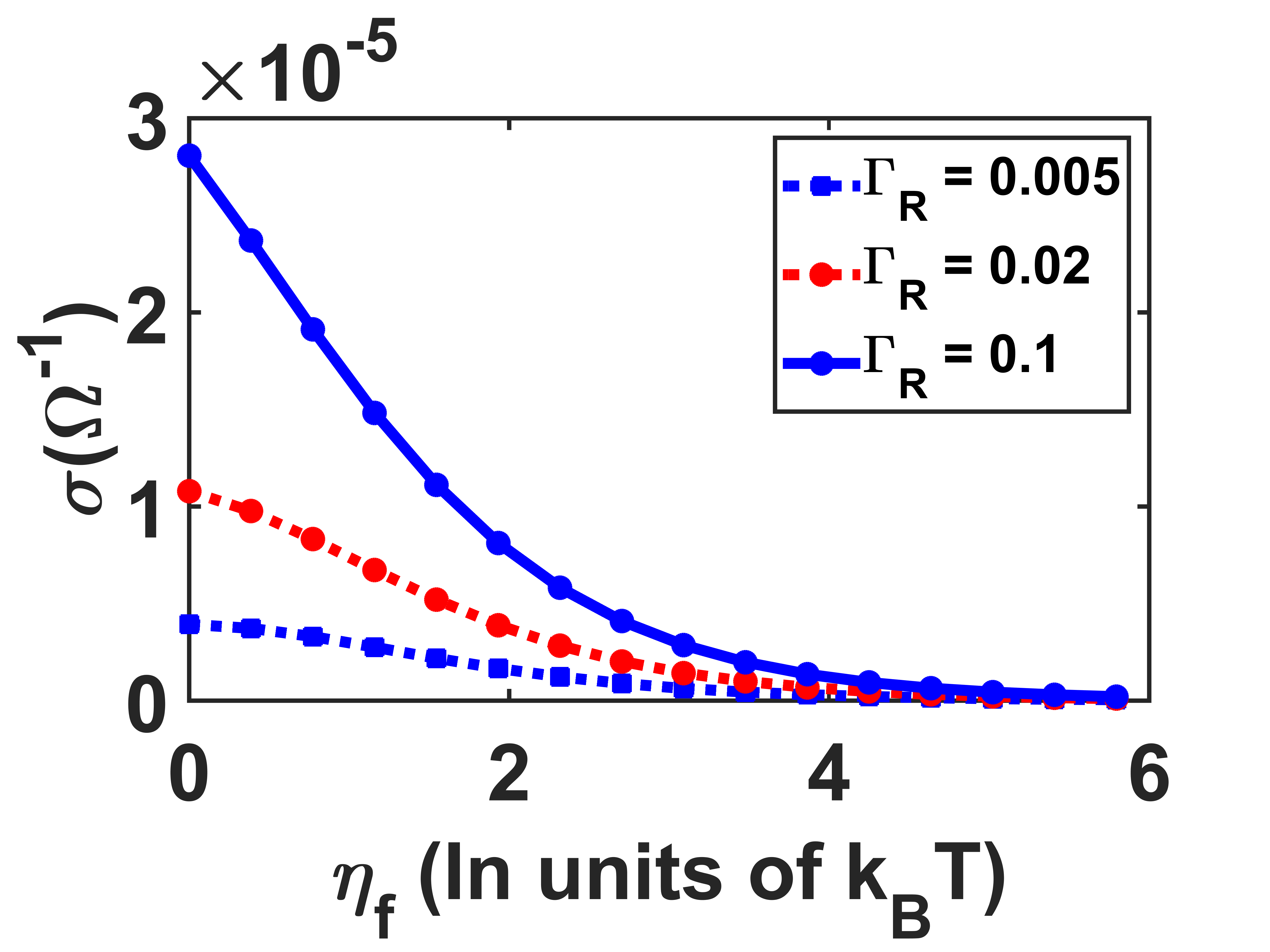
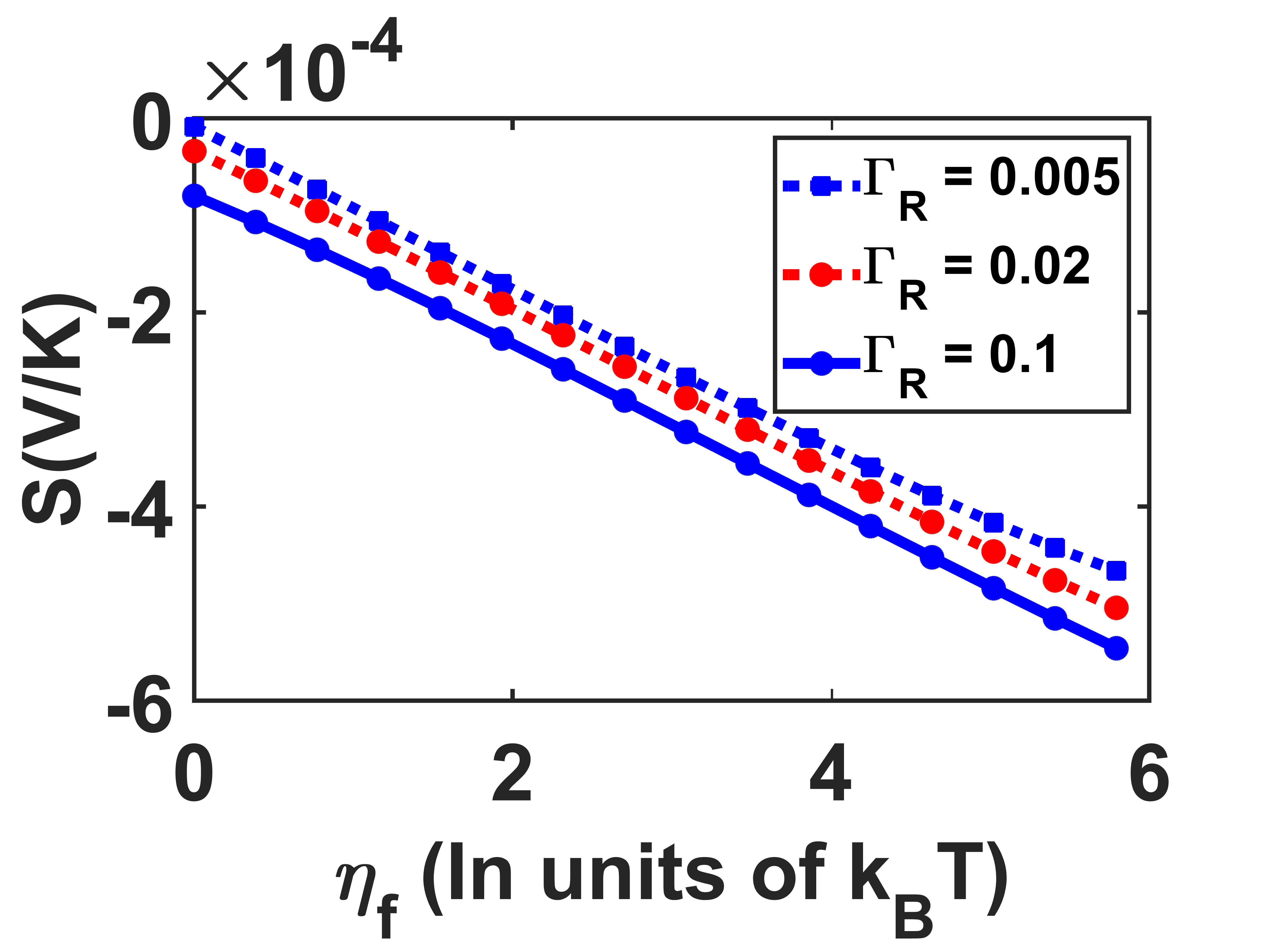
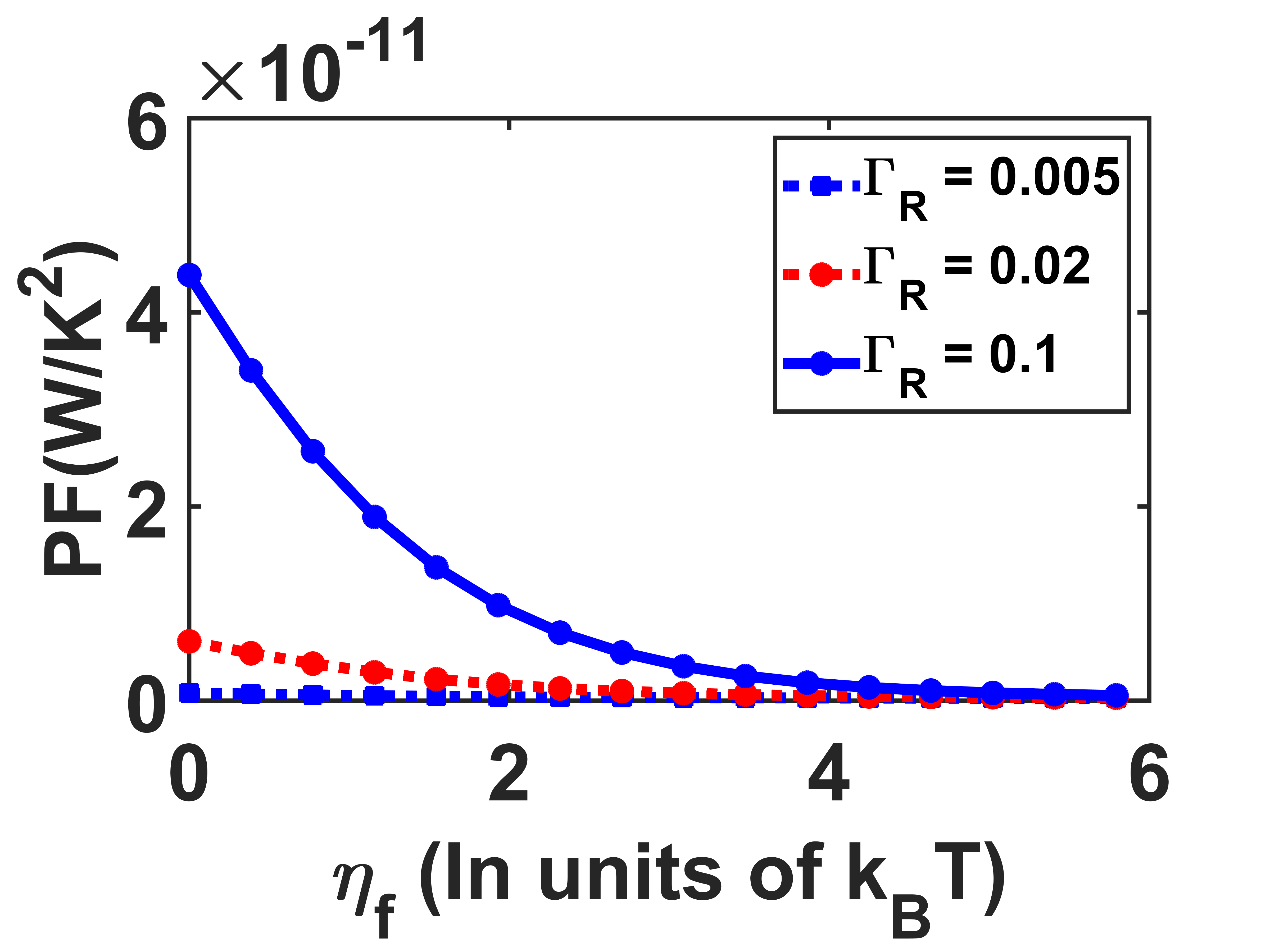
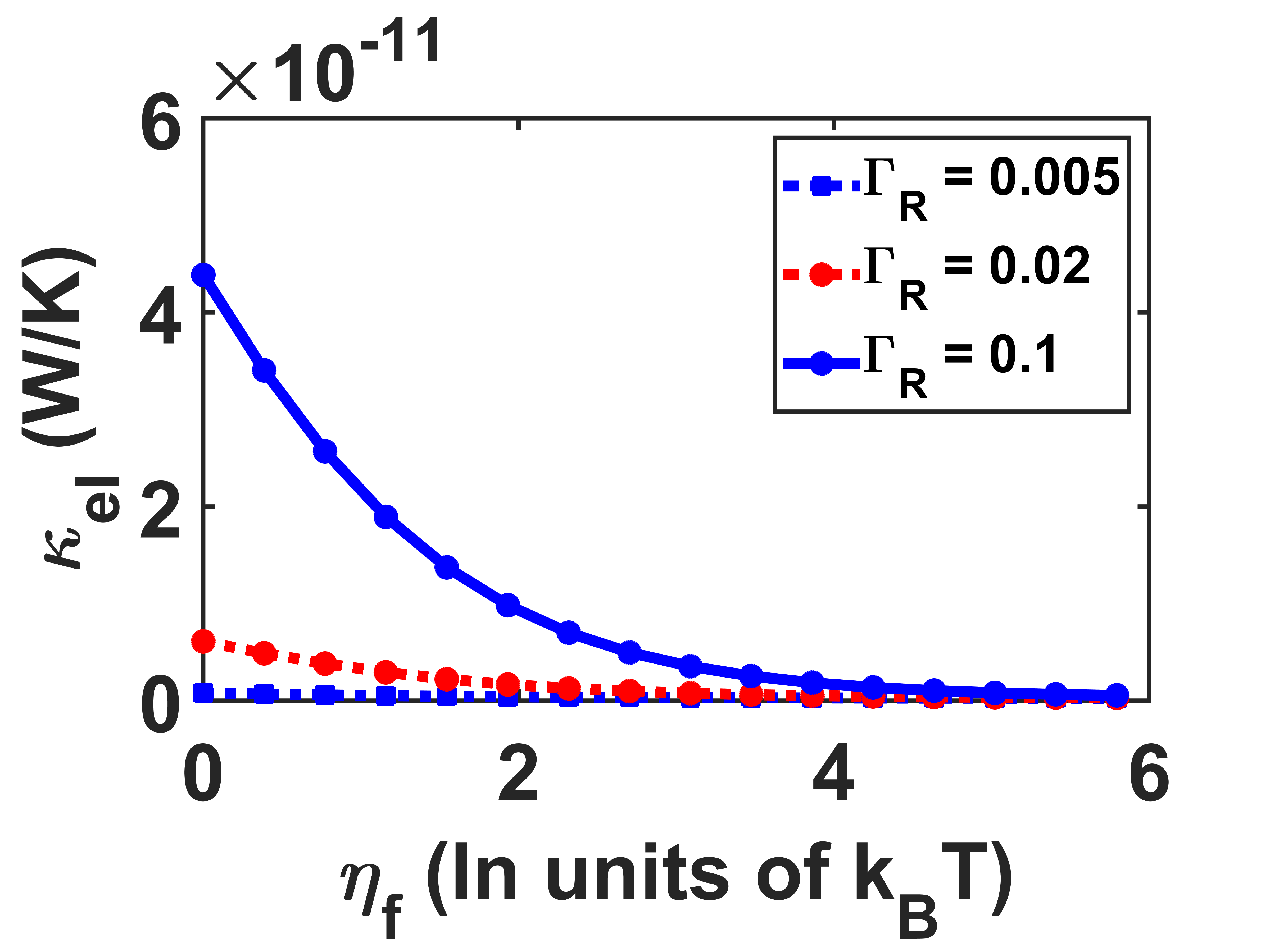
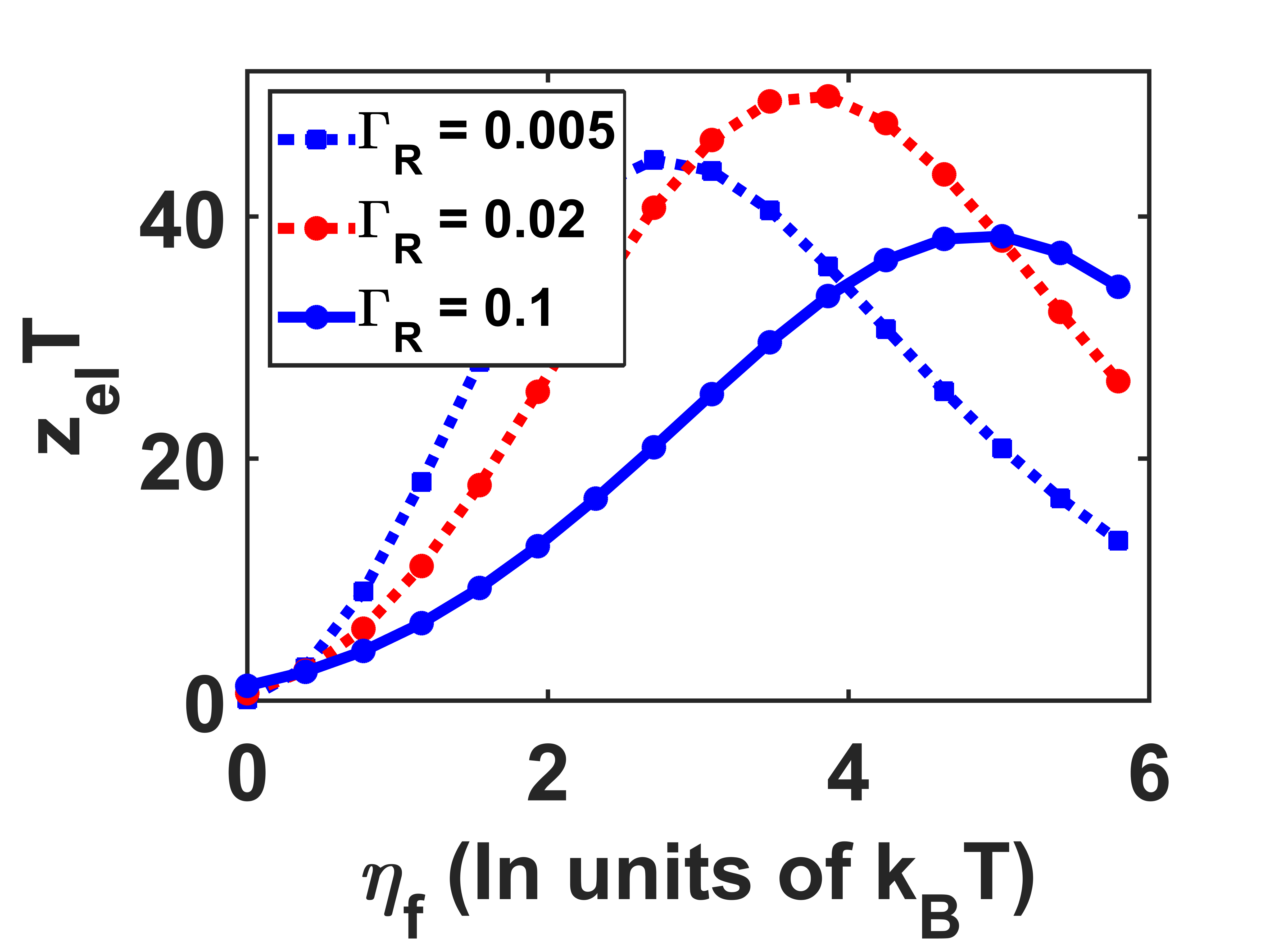
We plot in Fig. 4, the thermoelectric transport coefficients as a function of . We observe that for a fixed and , the transport coefficients decrease because of a reduced number of conduction channels. For a fixed , upon increasing , the conductivity decreases significantly as noted in Fig. 4(a). The Seebcek coefficient , however, does not show an appreciable decrease as noted in Fig. 4(b), while the electronic thermal conductivity decreases as noted in Fig. 4(d). These observations result in the trend of as noted in
Fig. 4(e). We observe that first increases and then decreases with increasing . Any 1D pristine material coupled with contacts will have the transmission to be a broadened step function which is achieved when . So we can conclude from Fig. 4(e) that for a given broadening due to coupling from the contacts, the asymmetric broadening results in the maximum that we can have. Therefore, in order to maximize , the trade-off between the three transport coefficients noted above explains the peaked behavior of .
So far, we have demonstrated in Fig. 4(e), that it is possible to get an improved via an electronic thermal conductivity decrease. We now need to be able to demonstrate such an effect in realistic super lattice structures. Given that a 1-D structure performs better, we focus on nano-ribbon based structures. In order to design such a structure we need to have control over the band gaps of the constituent materials. One method to control the material properties is to cut two dimensional sheets into ribbons or nano-pattern them Dobrik et al. (2008); Z. R. Dai et al. (2002); Aufray et al. (2010); Tchalala et al. (2014); Miro et al. (2014); Butler et al. (2013). Material properties of such structures are then strongly dependent on the geometry and can be used to form various super-lattice structures Gunlycke and White (2008); Fox et al. (2015); Wang et al. (2007). One such candidate for super lattice structures is graphene nano-ribbons, since the band gaps are dependent on the number of atoms along the width of the ribbon.
III.2 Graphene nano-ribbons
The band gaps for graphene nano-ribbon (GNR) follow three distinct trends depending on the number of atoms along the width , where, is some integer Gunlycke and White (2008). Due to computational complexity in implementing density functional calculations on such super-lattice structures, we have implemented a tight binding Hamiltonian for armchair graphene nano-ribbons using the third nearest neighbor with edge corrections (3NN-EC) described in Gunlycke and White (2008). The hopping parameters , , are used. We ignore the second nearest neighbor hopping as it is shown in Gunlycke and White (2008) the inclusion of second nearest neighbor interaction only shifts the complete band structure. The transmission function at each energy is then calculated using the ballistic non-equilibrium Green’s function (NEGF) formalism Datta (2005) within the tight binding Hamiltonian framework described above.
To validate our TB+NEGF implementation, we have compared our transmission plots with those obtained using density functional theory (DFT) for a set of armchair-GNRs. The results were within acceptable limits. The DFT calculations were done using the Atomistix packageBrandbyge et al. (2002); Soler et al. (2002); QW (3), which is based on the linear combination of atomic orbitals (LCAO) that use the spin polarized Peter-Wang functional within the local density approximation Perdew and Wang (1992) for the exchange correlation functional and the double-zeta double-polarized basis . The energy grid cut-off for the basis was set to with -point sampling of 100 points in the transport direction. Structural relaxation was done to a force tolerance of . The electron temperature was set to .
The transmission function is calculated from the bandstructure obtained using the method described in Jeong et al. (2010). The transmission spectrum is given by . Where transmission is assumed to be 1 i.e., we assume ballistic transport and is the Density of modes calculated using
| (6) |
where is the Heaviside step function. The above equation can simply be interpreted as counting the number of bands that cross a given energy in the direction perpendicular to the transport direction. Intuitively, it can be interpreted as counting the number of available parallel paths for electron transfer at a given energy.
III.3 Nano-ribbon-resonant tunnelling structure
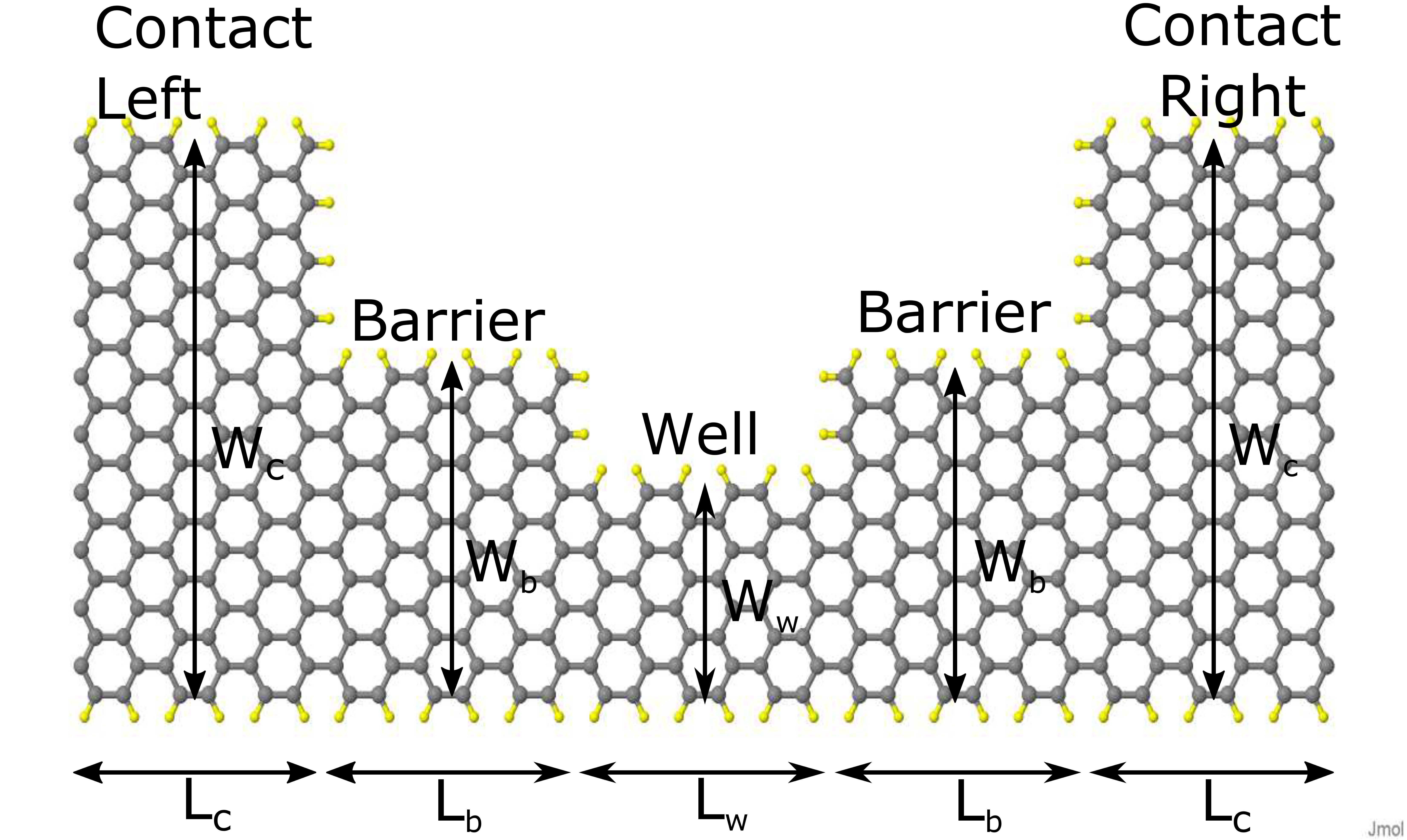
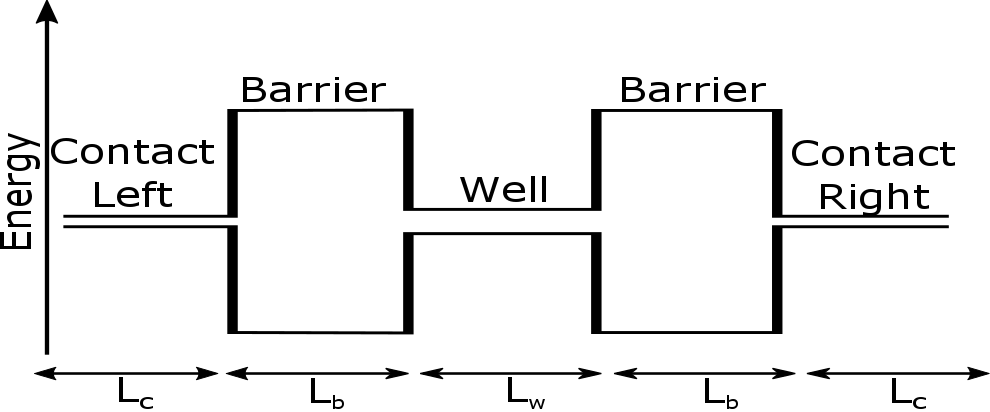
The schematic of the resonant tunnelling structure is shown in Fig. 1(a), and the band profile is schematically sketched in Fig. 5(b). Referring to Fig. 5(a), we can tune the transmission function by varying the length of the barrier, , the length of the well, , the width of the barrier nano-ribbon , and the width of well nano-ribbon . Here represents the number of atoms along the length and represents the number of atoms along the width.
As described earlier, the asymmetric delta peak can be obtained when the tail of delta distribution merges with the continuum. For this to happen, we should have the energy level which is very close to the top of the well. This can be achieved by having the well very shallow and narrow. As we increase the well depth, the allowed energy levels are deep inside which leads to a decreased broadening of the peak leading to a destruction in the asymmetry. Same is the case when we increase length of the barrier().
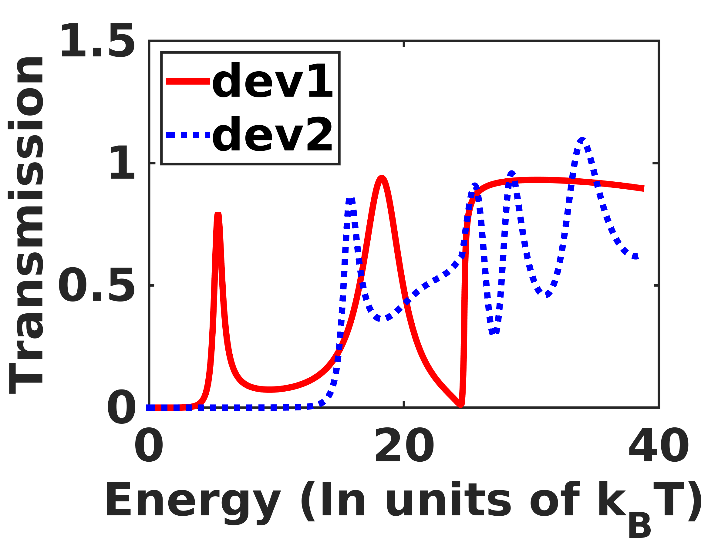
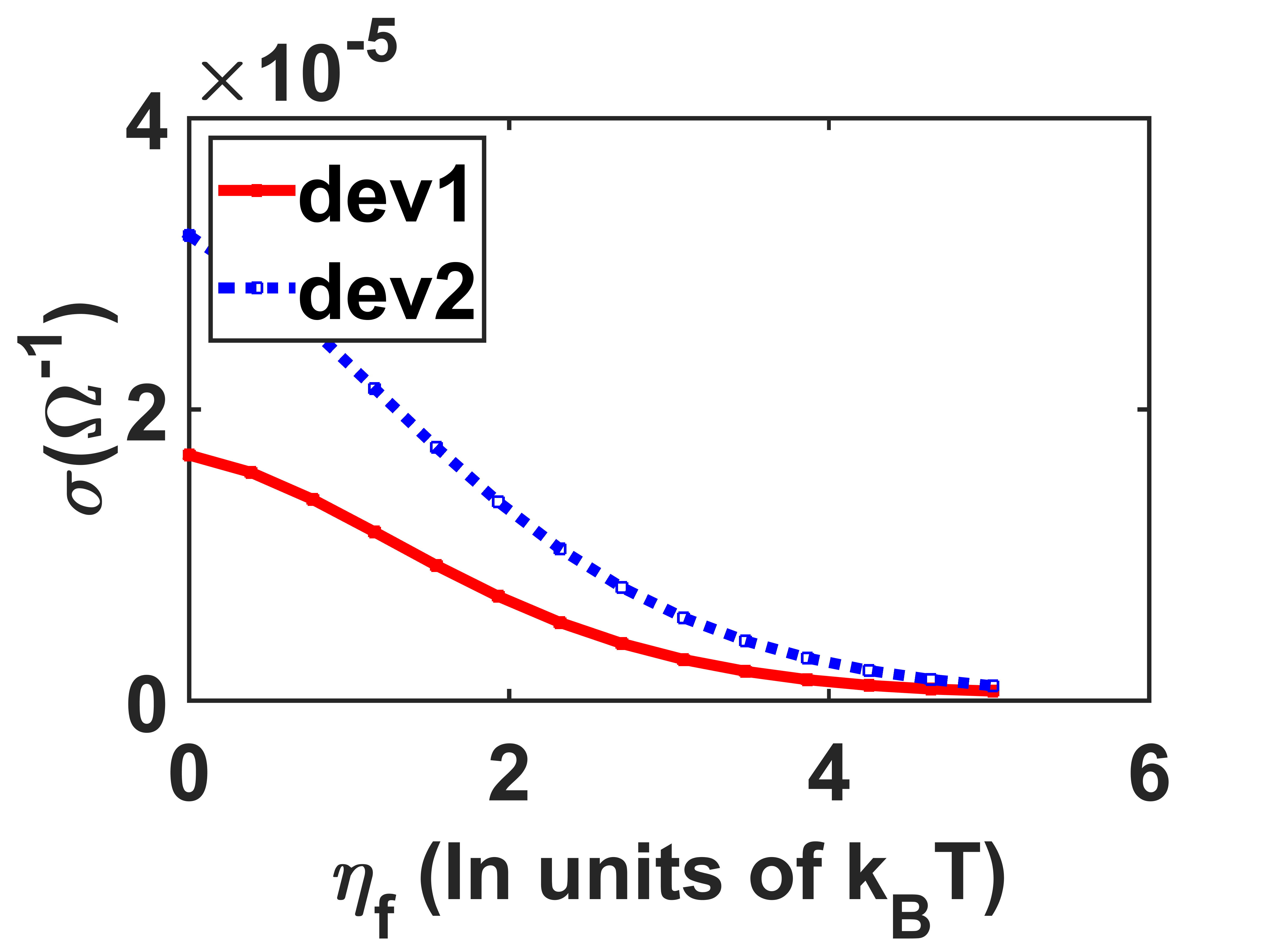
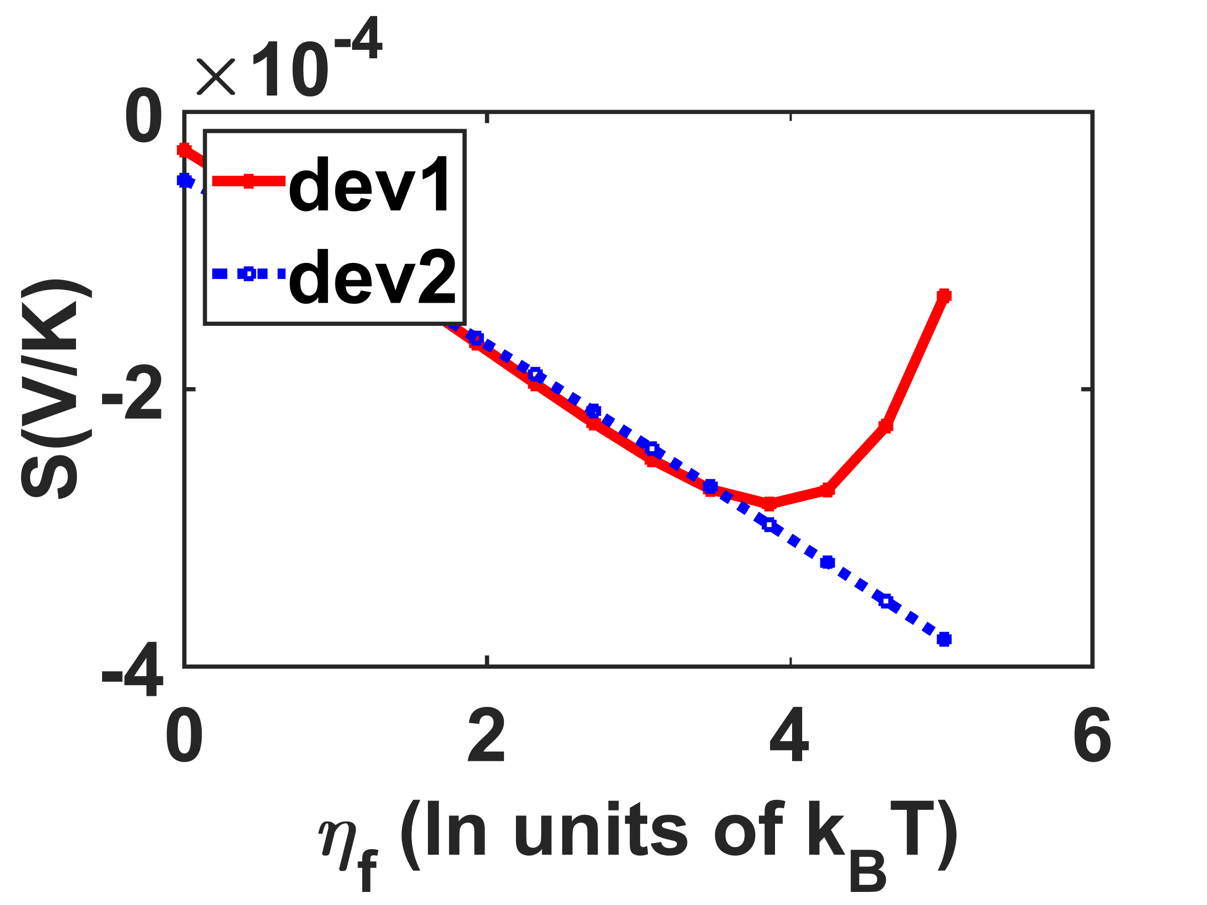
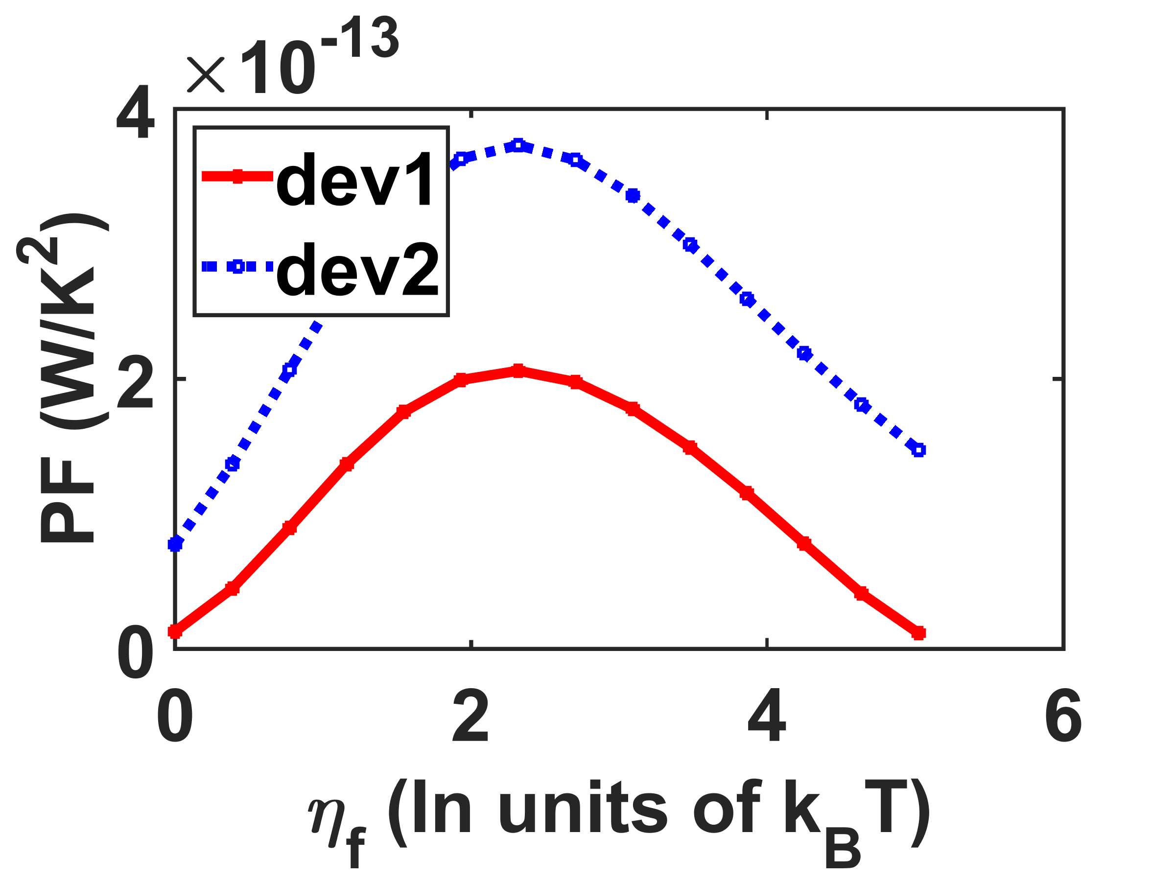
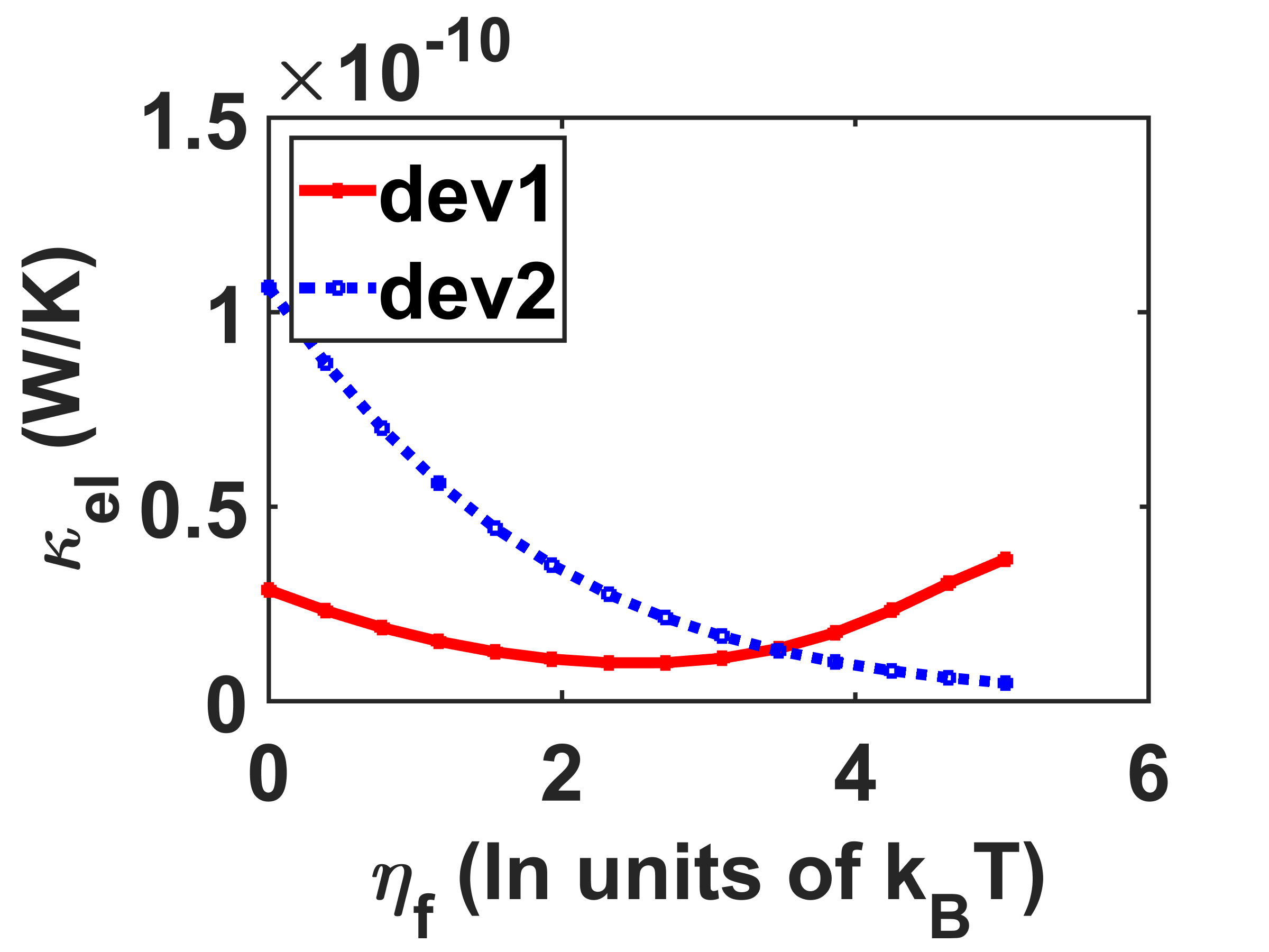
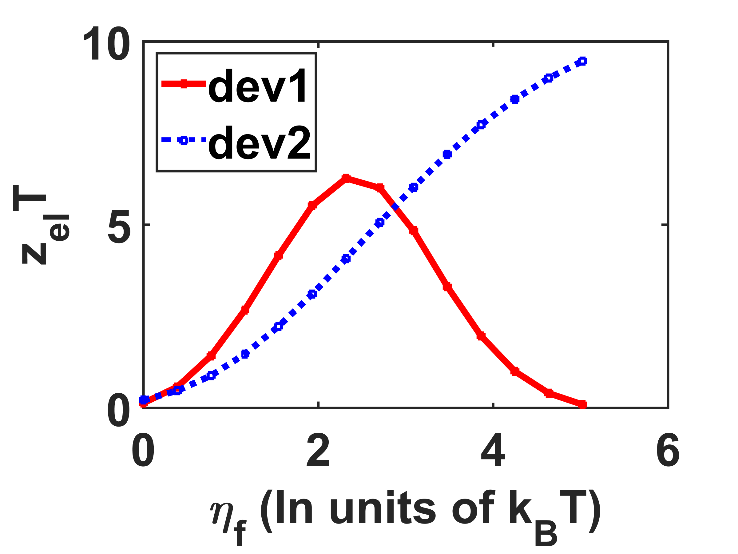
In Fig. 6(a), we depict the asymmetric delta function that results from armchair GNR based resonant structures. In both device-1 (dev1), with structural parameters , , , , and , and device-2 (dev2), with structural parameters , , , , and , we observe that the tail of the broadened delta function merges with the higher lying energy levels creating the asymmetry. In Fig. 6(c), we see that the variation in Seebeck coefficient is negligible with change in the device geometry. Similar to what we observed in the toy model in Fig. 4(b), we observe a sharp increase in the Seebeck coefficient in Fig. 6(d) after . This is because of the contribution of the valance band in the structure of the first device. Similarly, the trends for electrical conductivity and electronic thermal conductivity closely follow those observed in the toy model. Thus this enhancement in electronic figure of merit can be attributed to the drastic decrease in electronic thermal conductivity as compared to just the power factor , thus reinforcing the role of electronic thermal conductivity engineering. At this point, it is worth mentioning that some recent works on phonon scattering across 2-D interfaces Gunst et al. (2011); Mazzamuto et al. (2011); Sevinçli and Cuniberti (2010); Feng and Ruan (2016); Xie et al. (2016) have re-inforced a lattice thermal conductivity decrease due to the presence of interfaces typical to the structures explored here. Thus we can conclude further based on our work on lowering the electronic thermal conductivity and the aforesaid works on lattice thermal conductivity that the overall including the electron and lattice contributions is bound to increase in comparison to pristine systems.
IV Conclusion
To conclude, we have suggested an electronic thermal conductivity engineering route to increase the electronic figure of merit of nano-scale structures and demonstrated that this can be done using graphene nano-ribbons. While an idealized device with very small ambient quantum broadening may exhibit an ultra high , the realistic device structures explored here present a promising which may be further enhanced using structures designed using other emerging 2-D materials Butler et al. (2013) for which the band gaps can be precisely tuned to obtain the optimal broadening. The calculated figure of merit exceeding in such realistic structures further reinforces the concept and sets a promising direction to use nano-ribbon structures to engineer a favorable decrease in the electronic thermal conductivity. While high systems may not typically translate to high output power at high efficiencies Muralidharan and Grifoni (2012); Whitney (2014), such systems may be packaged to obtain a desired output power at a given efficiency Muralidharan and Grifoni (2012); Whitney (2014); Singha et al. (2015); Esposito et al. (2009a, b, 2010).
Acknowledgement: This work was in part supported by the IIT Bombay SEED grant and the Department of Science and Technology (DST), India, under the Science and Engineering Board grant no. SERB/F/3370/2013-2014.
References
- Hicks and Dresselhaus (1993a) L. D. Hicks and M. S. Dresselhaus, Phys. Rev. B 47, 12727 (1993a).
- Hicks and Dresselhaus (1993b) L. D. Hicks and M. S. Dresselhaus, Phys. Rev. B 47, 16631 (1993b).
- Dresselhaus et al. (2007) M. Dresselhaus, G. Chen, M. Tang, R. Yang, H. Lee, D. Wang, Z. Ren, J.-P. Fleurial, and P. Gogna, Advanced Materials 19, 1043 (2007).
- Snider and Toberer (2008) G. J. Snider and E. S. Toberer, Nature Mater. 7, 105 (2008).
- Mahan and Sofo (1996) G. D. Mahan and J. O. Sofo, Proc. Natl. Acad. Sci. U.S.A. 93, 7436 (1996).
- Heremans et al. (2008) J. P. Heremans, V. Jovovic, E. S. Toberer, A. Saramat, K. Kurosaki, A. Charoenphakdee, S. Yamanaka, and G. J. Snyder, Science 321, 554 (2008).
- Nakpathomkun et al. (2010) N. Nakpathomkun, H. Q. Xu, and H. Linke, Phys. Rev. B 82, 235428 (2010).
- Poudel et al. (2008) B. Poudel, Q. Hao, Y. Ma, Y. Lan, A. Minnich, B. Yu, X. Yan, D. Wang, A. Muto, D. Vashaee, X. Chen, J. Liu, M. S. Dresselhaus, G. Chen, and Z. Ren, Science 320, 634 (2008).
- Agarwal and Muralidharan (2014) A. Agarwal and B. Muralidharan, Applied Physics Letters 105, 013104 (2014).
- Nemir and Beck (2010) D. Nemir and J. Beck, Journal of Electronic Materials 39, 1897 (2010).
- Gunst et al. (2011) T. Gunst, T. Markussen, A.-p. Jauho, and M. Brandbyge, 155449, 1 (2011).
- Mazzamuto et al. (2011) F. Mazzamuto, V. H. Nguyen, Y. Apertet, and C. Ca, 235426, 1 (2011).
- Sevinçli and Cuniberti (2010) H. Sevinçli and G. Cuniberti, , 1 (2010).
- Feng and Ruan (2016) T. Feng and X. Ruan, Carbon 101, 107 (2016).
- Xie et al. (2016) Z.-x. Xie, L.-m. Tang, C.-n. Pan, K.-m. Li, and K.-q. Chen, 073105, 1 (2016).
- Shakouri (2011) A. Shakouri, Annual Review of Materials Research 41, 399 (2011).
- Faleev and Léonard (2008) S. V. Faleev and F. m. c. Léonard, Phys. Rev. B 77, 214304 (2008).
- Muralidharan and Grifoni (2012) B. Muralidharan and M. Grifoni, Phys. Rev. B 85, 155423 (2012).
- Humphrey and Linke (2005) T. E. Humphrey and H. Linke, Phys. Rev. Lett. 94, 096601 (2005).
- Esposito et al. (2009a) M. Esposito, K. Lindenberg, and C. Van den Broeck, Phys. Rev. Lett. 102, 130602 (2009a).
- Esposito et al. (2009b) M. Esposito, K. Lindenberg, and C. V. den Broeck, EPL (Europhysics Letters) 85, 60010 (2009b).
- Esposito et al. (2010) M. Esposito, R. Kawai, K. Lindenberg, and C. Van den Broeck, Phys. Rev. Lett. 105, 150603 (2010).
- Reddy et al. (2007) P. Reddy, S.-Y. Jang, R. A. Segalman, and A. Majumdar, Science 315, 1568 (2007).
- Sothmann et al. (2015) B. Sothmann, R. Sánchez, and A. N. Jordan, Nanotechnology 26, 032001 (2015).
- Jordan et al. (2013) A. N. Jordan, B. Sothmann, R. Sánchez, and M. Büttiker, Phys. Rev. B 87, 075312 (2013).
- Choi and Jordan (2015) Y. Choi and A. N. Jordan, Physica E: Low-dimensional Systems and Nanostructures , (2015).
- Lundstrom and Datta (2012) M. Lundstrom and S. Datta, Lessons from Nanoscience: A Lecture Note Series (World Scientific., 2012).
- Overhauser (1989) A. W. Overhauser, Applied Physics Letters 54, 2490 (1989).
- Datta (2005) S. Datta, Quantum Transport: Atom to Transistor (Cambridge University Press, 2005).
- Dobrik et al. (2008) G. Dobrik, P. Lambin, P. Biro, and L. Tapaszto, , 397 (2008).
- Z. R. Dai et al. (2002) Z. R. Dai, Z. W. Pan, and and Z. L. Wang*, The Journal of Physical Chemistry B 106, 902 (2002).
- Aufray et al. (2010) B. Aufray, A. Kara, S. Vizzini, H. Oughaddou, C. Léandri, B. Ealet, and G. Le Lay, Applied Physics Letters 96 (2010), http://dx.doi.org/10.1063/1.3419932.
- Tchalala et al. (2014) M. R. Tchalala, H. Enriquez, A. J. Mayne, A. Kara, G. Dujardin, M. A. Ali, and H. Oughaddou, Journal of Physics: Conference Series 491, 12002 (2014).
- Miro et al. (2014) P. Miro, M. Audiffred, and T. Heine, Chem. Soc. Rev. 43, 6537 (2014).
- Butler et al. (2013) S. Z. Butler, S. M. Hollen, L. Cao, Y. Cui, J. A. Gupta, H. R. Gutiérrez, T. F. Heinz, S. S. Hong, J. Huang, A. F. Ismach, E. Johnston-Halperin, M. Kuno, V. V. Plashnitsa, R. D. Robinson, R. S. Ruoff, S. Salahuddin, J. Shan, L. Shi, M. G. Spencer, M. Terrones, W. Windl, and J. E. Goldberger, ACS Nano 7, 2898 (2013).
- Gunlycke and White (2008) D. Gunlycke and C. T. White, Phys. Rev. B 77, 115116 (2008).
- Fox et al. (2015) D. S. Fox, Y. Zhou, P. Maguire, A. O’Neill, C. Ó’Coileáin, R. Gatensby, A. M. Glushenkov, T. Tao, G. S. Duesberg, I. V. Shvets, M. Abid, M. Abid, H.-C. Wu, Y. Chen, J. N. Coleman, J. F. Donegan, and H. Zhang, Nano Letters 15, 5307 (2015).
- Wang et al. (2007) Z. F. Wang, Q. W. Shi, Q. Li, X. Wang, J. G. Hou, H. Zheng, Y. Yao, and J. Chen, Applied Physics Letters 91 (2007), http://dx.doi.org/10.1063/1.2761266.
- Brandbyge et al. (2002) M. Brandbyge, J.-L. Mozos, P. Ordejón, J. Taylor, and K. Stokbro, Phys. Rev. B 65, 165401 (2002).
- Soler et al. (2002) J. M. Soler, E. Artacho, J. D. Gale, A. García, J. Junquera, P. Ordejón, and D. Sánchez-Portal, Journal of Physics: Condensed Matter 14, 2745 (2002).
- QW (3) Atomistix ToolKit version 2014.3, QuantumWise A/S (www.quantumwise.com) .
- Perdew and Wang (1992) J. P. Perdew and Y. Wang, Phys. Rev. B 45, 13244 (1992).
- Jeong et al. (2010) C. Jeong, R. Kim, M. Luisier, S. Datta, and M. Lundstrom, Journal of Applied Physics 107, 023707 (2010).
- Whitney (2014) R. S. Whitney, Physical Review Letters 112, 130601 (2014).
- Singha et al. (2015) A. Singha, S. D. Mahanti, and B. Muralidharan, AIP Advances 5, 107210 (2015).