Optical dependence of electrically-detected magnetic resonance in lightly-doped Si:P devices
Abstract
Electrically-detected magnetic resonance (EDMR) provides a highly sensitive method for reading out the state of donor spins in silicon. The technique relies on a spin-dependent recombination (SDR) process involving dopant spins that are coupled to interfacial defect spins near the Si/SiO2 interface. To prevent ionization of the donors, the experiments are performed at cryogenic temperatures and the mobile charge carriers needed are generated via optical excitation. The influence of this optical excitation on the SDR process and the resulting EDMR signal is still not well understood. Here, we use EDMR to characterize changes to both phosphorus and defect spin readout as a function of optical excitation using: a 980 nm laser with energy just above the silicon band edge at cryogenic temperatures; a 405 nm laser to generate hot surface-carriers; and a broadband white light source. EDMR signals are observed from the phosphorus donor and two distinct defect species in all the experiments. With near-infrared excitation, we find that the EDMR signal primarily arises from donor-defect pairs, while at higher photon energies there are significant additional contributions from defect-defect pairs. The optical penetration depth into silicon is also known to be strongly wavelength dependent at cryogenic temperatures. The energy of the optical excitation is observed to strongly modulate the kinetics of the SDR process. Careful tuning of the optical photon energy could therefore be used to control both the subset of spin pairs contributing to the EDMR signal as well as the dynamics of the SDR process.
I Introduction
Spin-based quantum phenomena at the nanoscale hold promise for the development of quantum-enhanced sensing and qubit-based computing architectures. In order to fully realize this potential, however, it is necessary to interface these phenomena to macroscopic scales. Isolated semiconductor dopants and defects offer long coherence times, robust and accurate quantum control and can be integrated into realistic device geometries. Some of the more intensively studied systems are nitrogen- and silicon-vacancy centers in diamond Staudacher et al. (2013); Rogers et al. (2014); Mamin et al. (2013), various defects in silicon carbide Falk et al. (2015); Calusine et al. (2016), as well as group V donors in silicon such as phosphorus Steger et al. (2012); Gumann et al. (2014); Hoehne et al. (2015), arsenic Franke et al. (2015) and bismuth Wolfowicz et al. (2013).
The most widely studied dopant in silicon is phosphorus (Si:P) which has a single naturally occuring spin-1/2 isotope 31P. The coherence times of this system are extremely long, up to seconds for electron spins and tens of minutes for the nuclear spins Tyryshkin et al. (2012); Saeedi et al. (2013), among the longest reported for spins in solids. Furthermore, the use of silicon offers the advantage of mature fabrication methods and ease of integration with commercial nanoelectronics, making it a nearly ideal system in which to engineer scalable quantum technologies Kane (1998); Hill et al. (2015), albeit at cryogenic temperatures ( K) to prevent ionization of the donor atoms.
Electrically-detected magnetic resonance (EDMR) of Si:P samples was first observed by Schmidt and Solomon over 50 years ago Schmidt and Solomon (1966) and has become an important tool for magnetic resonance of donors in micro- and nanoscale silicon devices due to its high sensitivity Stich et al. (1995); McCamey et al. (2006). EDMR in Si:P has been used to electrically detect donor spin states Stegner et al. (2006), and to readout an ensemble nuclear spin memory with extremely long lifetimes ( s) McCamey et al. (2010). Silicon EDMR has been integrated with photoconductive AFM into a scanning probe microscope Klein et al. (2013) and has been used to detect the protons from water adsorbed onto the silicon surface Dreher et al. (2015).
Multiple mechanisms are known to mediate the spin-dependent transport that enables EDMR in different experimental configurations Kaplan et al. (1978); Honig and Lagnado (1970); Ghosh and Silsbee (1992). At low fields ( T) where the longest coherence times have been observed, the dominant mechanism is spin-dependent recombination (SDR), where the recombination of a pair of spins depends on their spin permutation symmetry. Resonant excitation of either spin changes this symmetry, modulating the current through the device. In Si:P, such spin pairs can be formed by phosphorus donors and paramagnetic defects located at the Si/SiO2 interface, between pairs of defects or even between pairs of donors at higher doping concentrations Stegner et al. (2006); Hoehne et al. (2010, 2013). At cryogenic temperatures and low-doping concentrations, optical excitation is used to generate the free carriers necessary for EDMR. The influence of this optical excitation on the SDR rates and the observed EDMR signal is still not well understood. While most EDMR experiments have used white light sources for the optical excitation Stegner et al. (2006); McCamey et al. (2006, 2008); Morishita et al. (2009); Hoehne et al. (2010); Lee et al. (2010), light emitting diodes Hoehne et al. (2013, 2015) and laser excitation Stich et al. (1995) have also been used. At cryogenic temperatures the optical penetration depth of light into silicon is known to be strongly wavelength dependent Macfarlane et al. (1958). Thus both the kinetic energy and the spatial distribution of the photo-excited carriers changes with wavelength. Broadband optical excitation, for example, generates both hot carriers along with near-band-edge carriers – with differing spatial distributions.
Here, we investigate the wavelength dependence of the EDMR signal in a Si:P device, using three different optical sources: a 980 nm laser whose energy is just above the band edge of silicon at cryogenic temperatures, a 405 nm laser to generate hot surface-carriers, and a broadband tungsten-halogen lamp white light source. With near-infrared excitation, we find that the EDMR signal primarily arises from donor-defect pairs, while at higher photon energies there are significant additional contributions from defect-defect pairs. Using frequency modulated (FM) continuous-wave (CW) EDMR we measure the modulation frequency and microwave power dependence of the EDMR signal for each optical excitation and show that the optical excitation energy can strongly modulate the kinetics of the SDR process. Careful tuning of the optical photon energy could therefore be used to control both the subset of spin pairs contributing to the EDMR signal as well as the dynamics of the SDR process.
II Spin Dependent Recombination
If a sample of Si:P is irradiated with above gap light at low temperatures, a steady-state photocurrent is generated where the optical excitation rate is balanced by the carrier recombination rate. If any of the recombination pathways is spin-dependent, a resonant excitation of the spins can modulate the recombination rate and transiently change the current through the sample, a mechanism proposed by Kaplan, Solomon and Mott Kaplan et al. (1978).
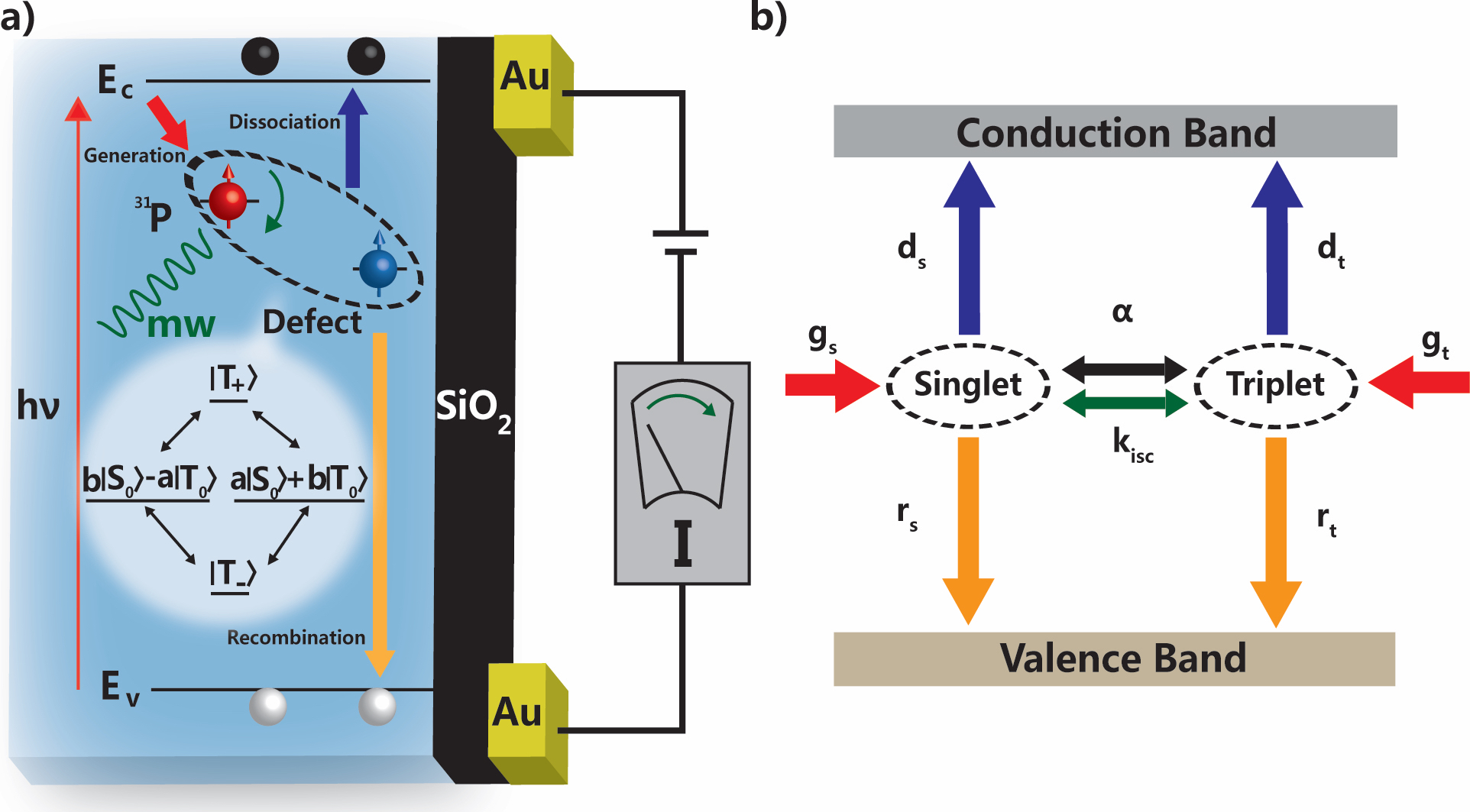
Figure 1(a) illustrates the basic EDMR experiment in Si:P. Shallow phosphorus donor electrons near the Si/SiO2 interface interact with adjacent (deep) paramagnetic defects present at the interface via either dipolar or exchange interactions. The four energy eigenstates for the spin pair are , , and the two admixed states and , where and are the triplet and singlet states. For a strongly-coupled pair, the states and become the singlet state and the triplet state (), while for very weak coupling they become the product states and ().
Since silicon has low spin-orbit coupling, the recombination process is spin-preserving, resulting in faster recombination rates for states with singlet character compared to states with triplet character. During steady state optical excitation, most pairs are pumped into the states or , since all the states are generated at the same rate (by non-geminate carriers) but and can recombine relatively quickly, given their singlet content. Resonant microwave excitation of either spin can induce transitions from states and to states or , resulting in a change in current.
Lee et al. proposed a two-component (singlet/triplet) kinetic model to describe the signal dependence observed in CW EDMR experiments that takes into account the competing generation, recombination and dissociation processes Lee et al. (2012). Figure 1(b) illustrates the key parameters of this model. Under optical excitation, spin pairs are randomly generated in each of the four above configurations with equal probability, so that the singlet and triplet generation rates and are related by . The singlet and triplet populations dissociate at rates and , releasing an electron to the conduction band, and recombine at rates and , when one of the electrons in the pair recombines with a hole in the valence band. Transitions between the singlet and triplet manifolds can be induced by either microwave excitation or via relaxation processes. To lowest order, the microwave-induced transition rate is proportional to the microwave power, while relaxation to thermal equilibrium populations is assumed to occur at a rate via inter-system crossover. Assuming a simple on-off amplitude modulation scheme, they derived a set of coupled differential equations describing the changes to the free carrier populations and the current through the device. The key equations describing the model are shown in Appendix A.
While the SDR mechanism for phosphorus donors is believed to primarily be mediated by mid-gap dangling-bond Pb0 defects Poindexter (1981); Stesmans and Afanas‘ev (1998); Stegner et al. (2006); Hoehne et al. (2010), previous EDMR measurements have measured E’ defects Lee et al. (2010) as well as Pb1 defects and a central donor pair resonance Hoehne et al. (2010). It was recently shown that EDMR in Si:P is primarily sensitive to those donors located within roughly the first 20 nm of the Si/SiO2 surface Suckert et al. (2013). The properties of a single donor-defect pair were also recently characterized using scanning probe techniques Ambal et al. (2016).
III Experimental Setup
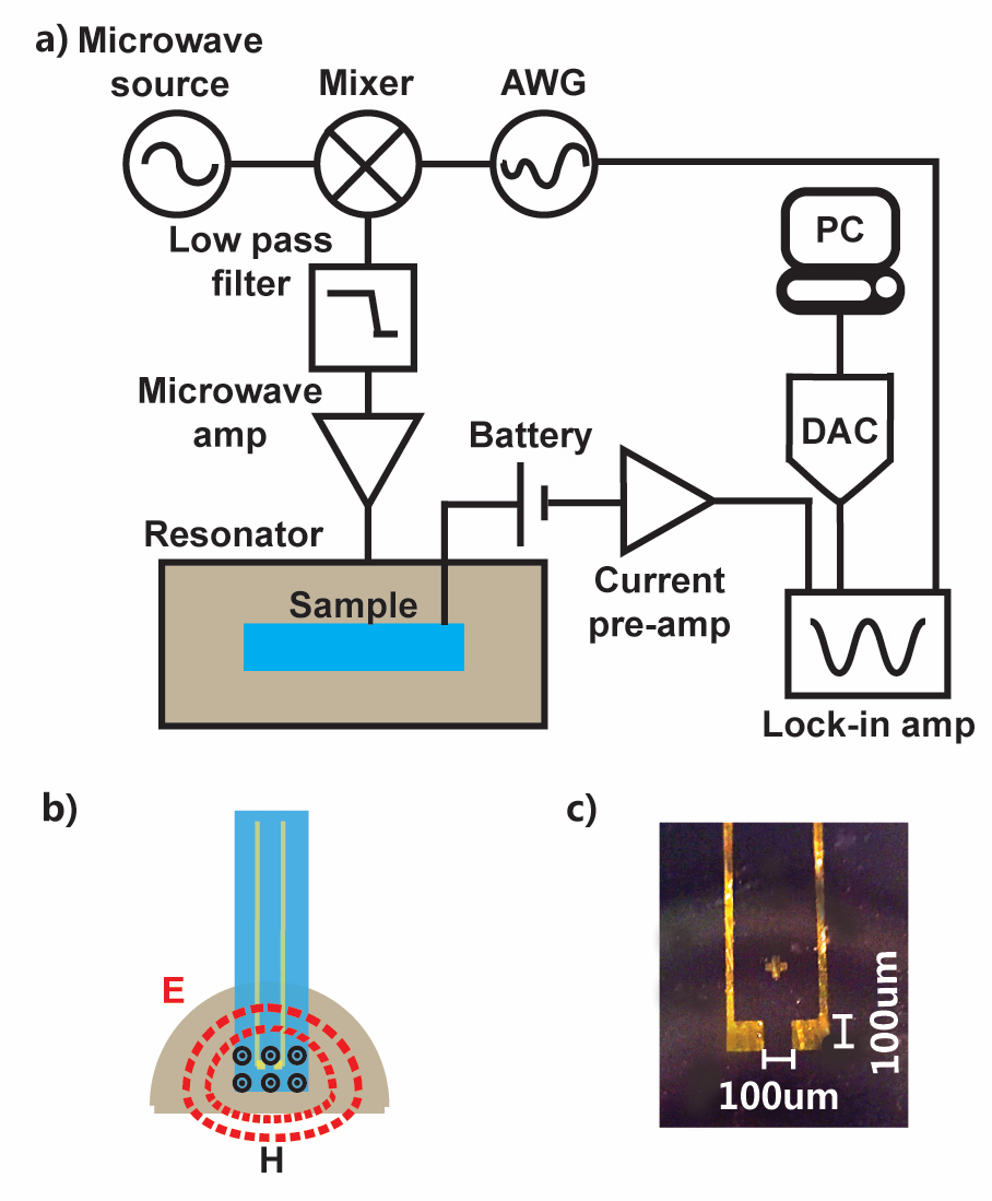
Figure 2(a) shows a schematic of the experimental setup used. The static magnetic field was generated by a 3-inch diameter electromagnet (Spectromagnetic Model 1019). A microwave synthesizer (QuickSyn FSW-0020) provided a constant carrier frequency of 2.596 GHz, which was mixed (Marki T3-06LQP) with a discrete, numerically-generated, frequency-modulation (FM) or amplitude-modulation (AM) waveform loaded into a high-frequency arbitrary waveform generator (Tektronix AWG7052). Low-pass filtering (Mini-Circuits VLF-2250+) was used to attenuate the upper sideband and carrier components by approximately 20 dB. The microwaves were then amplified by 30 dB (Mini-Circuits amplifiers ZX60-V62 and ZX60-6019 in series), before being transmitted to the sample. The microwaves were coupled to the sample with a lab-built, low quality-factor (), stripline-fed dielectric antenna mounted on the cold-finger of a continuous-flow Janis optical cryostat.
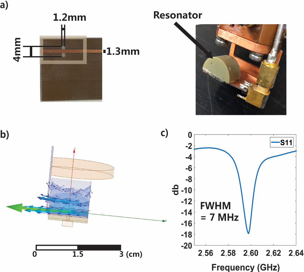
Figure 2(b) shows the mode structure of the half-cylinder dielectric antenna used in the experiment (described in more detail in Appendix B). The relative alignment of the sample and antenna was set to minimize RF electric-field () coupling to the electric current () through the device (), since such a coupling can excite microwave-induced currents that could mask the spin-dependent current changes. The stripline-fed dielectric resonator had a 3 dB bandwidth of 7 MHz, centered at 2.596 GHz, resulting in a of 371 at K.
A battery and resistor network were used to provide a constant bias current, , for a given optical illumination of the Si:P device. The current was fed to an SRS 570 current amplifier, which also compensated for the constant current bias. With 405 nm and white light excitation, the signals were measured in low-noise mode with a sensitivity setting of A/V, while the high-bandwith mode and a A/V sensitivity were used with the 980 nm excitation. No additional filtering was performed in the current preamplifier. The output of the current amplifier was connected to an SRS 830 lock-in amplifier, to which the FM (or AM) waveform was input as a reference, and whose resulting output was digitized using a National Instruments NI-USB-6361 DAQ. The time constant on the SR 830 was set to 100 ms in all the experiments described here.
The sample used in the experiment was fabricated on a commercial silicon on insulator (SOI) wafer (Ultrasil Corporation). The lightly phosphorus doped wafer had a device resistivity of 1-4 cm in the 100 orientation, which corresponds to a phosphorus doping concentration of cm-3. This is significantly lower than the cm-3 phosphorus donor concentrations used in most previously reported EDMR experiments 111While Stich, et al. used samples with a donor concentration of cm-3, they were unable to see an EDMR signal without irradiating the sample with 2 MeV electrons Stich et al. (1995), thereby generating bulk donor-defect pairs, where exchange interactions between the donors begins to become significant Cullis and Marko (1975). The sample was mounted with the wafer parallel to the magnetic field.
The 2.00.5 m thick device layer is located on a 1 m buried oxide layer. The 50010 m thick handle layer is boron doped with a resistivity of 10-20 cm in the 100 orientation. The native oxide surface layer has a thickness 10 nm. Gold contacts (100 nm) were thermally evaporated onto the surface, creating a 100 m junction as shown in Figure 2(c) (Additional processing steps are described in Appendix C). This corresponds to an active device volume (assuming a sensitive depth of 20 nm) on the order of cm3 containing about donor electron spins. The typical surface density of both and E’ defects is in the range of cm-2 Lenahan and Conley Jr. (1998); Hervé et al. (1992); Takahashi et al. (1987), leading to an estimate of about defect spins in the active device area.
IV Results and Discussion
IV.1 Microwave Modulation
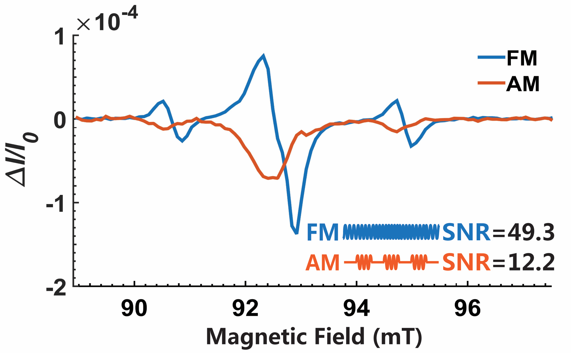
Although magnetic field modulation has traditionally been used for lock-in detection of CW-ESR and CW-EDMR, the use of small modulation coils (both to minimize inductance and due to space constraints) can lead to larger magnetic field inhomogeneities Crosser et al. (2010). Additionally, vibrations due to Lorentz forces and direct inductive pickup of the field modulation by the electrical leads can lead to increased noise in EDMR signals. AM microwave can also be used to detect EDMR, but the microwave-induced currents in the device electrode also pick up the modulation frequency and can mask the true EDMR signal as described in the previous section. For FM microwave modulation, the -field coupling to the sample can be minimized since the microwave induced current is constant over the range of modulation frequencies, so that the modulation envelope is only transferred into the signal under magnetic resonance conditions. Here, a triangular envelope was used for the FM frequency variation, with the maximum frequency deviation set to 12 MHz, slightly larger than the measured resonator bandwidth.
Figure 3 shows a comparison between FM EDMR spectra (blue) and AM EDMR spectra (red) using a 1 kHz modulation frequency under white light excitation. The central peak is due to surface defects while the two outer lines correspond to the 4.2 mT ( MHz) hyperfine split lines of the phosphorus donors () Stegner et al. (2006); Morishita et al. (2009). The transconductance gain of the current preamplifier was used to calculate the fractional current change from the measured signal voltage. Note that, although FM EDMR results in derivative lineshape spectra, AM EDMR does not. The peak microwave power delivered to the sample was kept constant at 3.16 W in both experiments. Part of the difference in peak signal intensity between the two spectra is likely due to the lower average microwave power (a factor of 3 for a symmetric triangular waveform) in the AM experiment. However, the signal-to-noise ratios (SNR) measured in the two experiments differ by a factor of 4, indicating a superior sensitivity for FM over AM EDMR. Typical resonant changes in device current of are observed.
IV.2 Optical Selection of Spin-Pair Species
Figures 4(a), (b), and (c) show the EDMR spectra recorded using a 25 mW 405 nm laser ( eV; Edmond Optics 59562), a 6 W broadband white light source (OceanOptics LS-1-LL), and a 200 mW 980 nm laser ( eV; ThorLabs L980P200) respectively. Under the same bias conditions, the induced photocurrent () in the sample was 5 A for the blue laser, 40 nA for the infra-red laser, and 1 A for the tungsten halogen lamp. For bias voltages under 5 V, the leakage current in the dark was negligible. The microwave power used in these experiments was 3.16 W, which is sufficient to saturate the EDMR spectra, as shown later.
The (peak-to-peak) fractional current change for the phosphorus donors () changes from at 405 nm illumination to about for 980 nm and for white light illumination. The intensity of the central defect peak depends much more strongly on the optical excitation, with changing from at 405 nm to under white light and at 980 nm. The ratio between the two signals changes from at 405 nm to with white light and at 980 nm. Table 1 summarizes these results. This change in the ratio between the two signals suggests that additional defect-defect interactions are contributing to the EDMR signal under 405 nm excitation. The area of the defect peak is greater than the sum of the two hyperfine split phosphorus peaks in all the experiments.
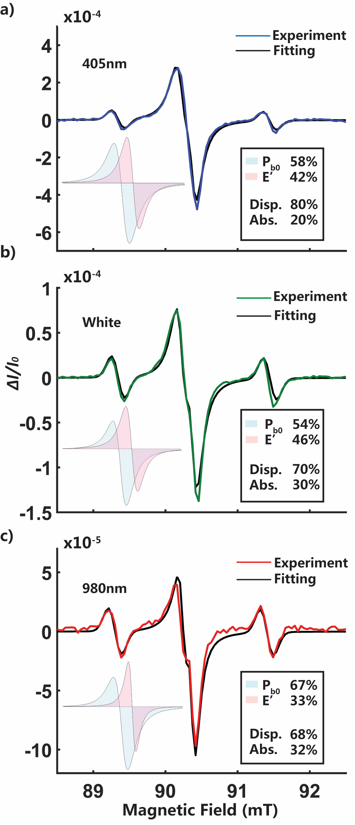
At the low donor concentrations used here, we do not expect donor pair resonances to arise. However multiple donor-defect and defect-defect EDMR signals are likely to be present. The figures also show the result of a spectral fit. The 117.4 MHz hyperfine-split phosphorus peaks were used to calibrate the field, with the -factor of the phosphorus peak set to =1.9985. The center defect peak was fit to the sum of two Lorentzian lines. One of the peaks has a -factor of 2.0002 which is close to the reported value ( = 2.0005) of deep hole oxide trap E’ defects Lenahan and Conley Jr. (1998). The other peak has a -factor of 2.0058 which is intermediate between the -values reported for Pb0 ( - parallel to (111); ; - parallel to (011)) and Pb1 (; - parallel to (111); - parallel to (011)) at the orientation used in the experiment Poindexter (1981); Lenahan and Conley Jr. (1998). We have labeled this the Pb0 defect since this is the most-commonly observed defect peak in EDMR. The shifts in the observed -factor are most likely due to errors in sample alignment with the field. The peak is also observed to have a mixed absorptive and dispersive character. Zevin and Suss have shown that such distortions of the line-shape can be caused by the microwaves passing through conducting metallic or semiconducting layers Zevin and Suss (1986). The dispersive component could arise from defect spins in the buried oxide layer. The distortion in the line-shape is more obvious under 980 nm excitation where the optical penetration is the greatest. The contribution of the E’ signal also drops while that of the Pb0 signal increases for the long wavelength excitation. This suggests that the observed E’ defects are primarily located on the top surface while the Pb0 defects are present at both the surface and buried oxide layers.
The width of the phosphorus peaks ( G) and the Pb0 peak ( G) remained relatively unchanged in the different experiments. The width of the E’ peak changed from G for 405 nm and white light excitation to G for 980 nm excitation. This is consistent with a weaker perturbation of the surface E’ spins with long wavelength excitation.
| Source | P0 | PI | P2μm | I0 | P20nm | ||||
|---|---|---|---|---|---|---|---|---|---|
| (mW) | (mW) | (mW) | (A) | (m) | (mW) | ( | ( | ||
| 980 nm | 200 | 63.7 | 1.2 | 0.04 | 100 | 0.012 | |||
| white | 6000 | 1910 | - | 1 | - | - | |||
| 405 nm | 25 | 8 | 8 | 5 | 0.12 | 1.2 |
Given the nominal incident powers and taking literature values for silicon absorption coefficient at these wavelengths Green and Keevers (1995), the calculated absorbed optical power over the device active volume ranges from 12 W at 980 nm to 1.2 mW at 405 nm. However, the induced steady-state photocurrent () is likely to pass uniformly through the entire 2 m device layer for the 980 nm excitation, given the 100 m penetration depth, but be more inhomogeneously distributed for the 405 nm excitation. While the optical penetration is restricted to about 120 nm at this wavelength, the carriers are likely to diffuse through the entire 2 m device layer. However the surface contribution to the overall current will be significantly higher for the 405 nm excitation than for the 980 nm excitation. This suggests that the fractional current changes could be made much larger using excitation in the infra-red if the current paths could be constrained to the surface, as has been done with the use of epitaxially-grown silicon layers Suckert et al. (2013).
The excess energy of the incident photons relative to the silicon band-gap is rapidly dissipated through electron and phonon scattering that can significantly modify the kinetics of the SDR process. At 4.2 K, silicon possesses two thresholds for indirect band-gap transitions, with the higher at 1.2135 eV Macfarlane et al. (1958). As a consequence, the types of carriers excited under each illumination varies widely. Excitation at 980 nm, just above the second phonon-mediated absorption threshold, generates relatively low-energy carriers, while 405 nm excitation leads to absorption enhancement of nearly three orders in magnitude Jellison (1982), generating hot carriers and increasing the phonon bath. The broadband white light source spans both regimes, while also exciting sub-band transitions such as donor-bound excitonic transitions, as have recently been exploited to perform bias-free EDMR experiments in isotopically-enriched silicon-28 samples Steger et al. (2012); Saeedi et al. (2013).
| Defects | Phosphorus | |||||
|---|---|---|---|---|---|---|
| Source | 405nm | White | 980nm | 405nm | White | 980nm |
IV.3 Wavelength-Dependent Rate Changes
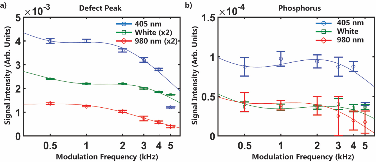
In order to better connect to the changing kinetics of the SDR process, we measured the modulation frequency and microwave power dependence of the EDMR signal for each optical excitation. Figure 5(a) and (b) show the modulation frequency dependence of the phosphorous donor and overall central defect signal intensities. The current change is observed to decrease at higher modulation frequencies in all cases. The change in EDMR with modulation frequency is an indirect probe of the SDR kinetics Hoehne et al. (2013); Lee et al. (2012). The solid lines in Figure 5 show the simulated signal dependence predicted by the kinetic model of the EDMR process described earlier Lee et al. (2012). Note that while this model was developed for a simple on-off amplitude modulation of the EDMR signal, we are using it here to approximately describe the triangular frequency modulation signal measured in our experiments. Table 2 shows the parameters in these simulations. Dreher et al. have reported singlet and triplet recombination time constants to be 15 s and 2 ms respectively in Si:P Dreher et al. (2015). However the other rates for this system have not been measured to date. Our initial estimate for these kinetic parameters were taken from Ref. Lee et al. (2012). We assumed these rates would not change by more than an order of magnitude, thus keeping the general shape of the modulation dependence the same. Appendix D outlines the detailed data processing steps and the calculation of the error bars shown.
In general, we see that almost all the electronic rates for both defects and phosphorus signals are higher for the 405 nm excitation experiment. For the defect signal, the singlet recombination rate at 405 nm is a factor of 2 higher than the rate at 980 nm or with white light excitation. Overall the electronic recombination and dissociation rates for the defect signal are observed to be higher than for the phosphorus signal. However, the model fails to capture the signal decrease at the highest modulation frequency under 405 nm excitation. This is probably due to the fact the observed signal arises from a number of different spin pairs, while the simulations are performed on a single pair. The central defect signal could have contributions from Pb0-Pb0, Pb0-E’, E’-E’, Pb0-Phosphorus and E’-Phosphorus pairs. Appendix E shows the change in the different defect components as a function of modulation frequency. It should be noted that these signals still represent the average behavior of multiple spin species, and could be partially correlated with each other.
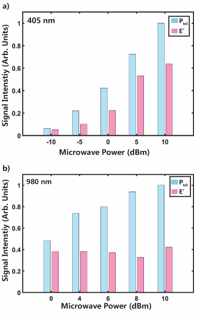
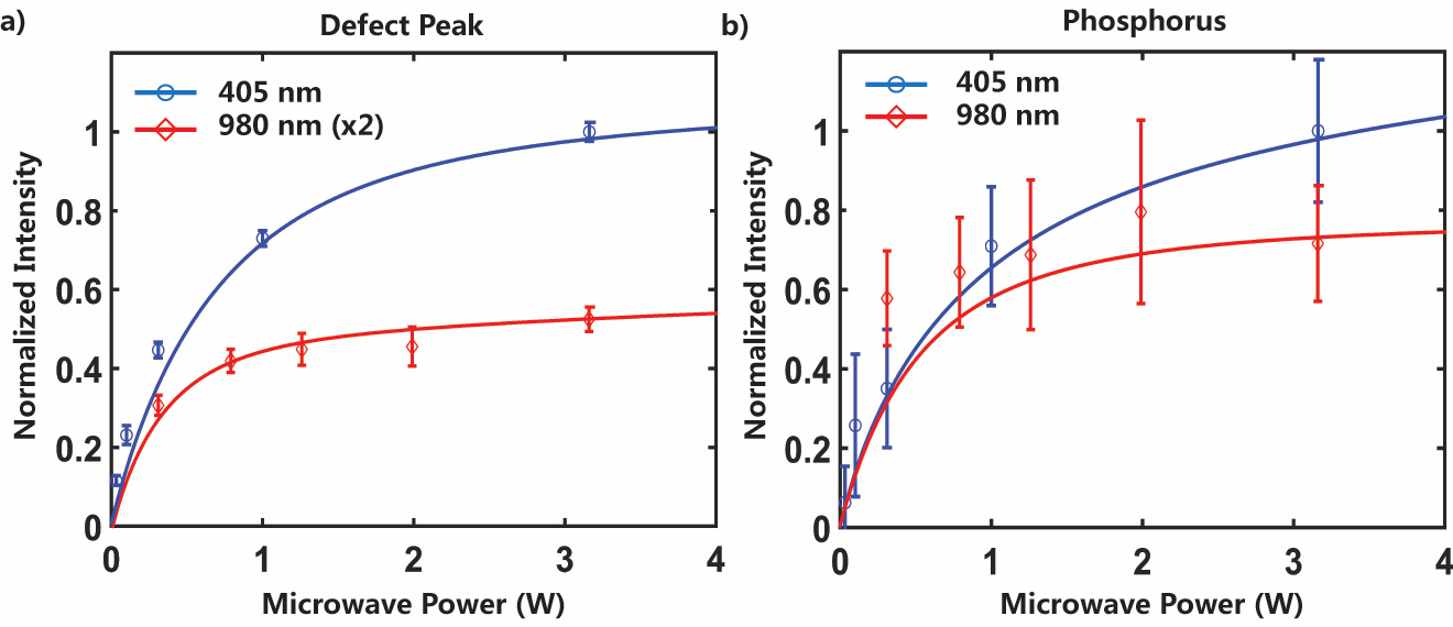
Figures 6(a) and (b) show the microwave power dependence of the two components for the blue and red laser excitation, showing that the fractional current change initially increases with microwave power before saturating, as has been observed previously Stich et al. (1995). To match the curves in Figure 6 the parameter was varied (assumed directly proportional to power) while all other parameters were kept fixed.
Care should be taken in interpreting the above changes in rate constant quantitatively, as Lee et al. have shown that a wide range of combinations of electronic rates can give rise to the same modulation frequency dependence Lee et al. (2012).
V SUMMARY and OUTLOOK
In summary, we have demonstrated high-sensitivity FM EDMR in lightly-doped Si:P devices, making comparative measurements on the optical excitation dependence of the EDMR spectra. We find that photon energies just above silicon’s phonon-mediated absorption threshold lead to a spin-spin population dominated by dopant-defect pairs, while the generation of hot carriers greatly increases the population fraction of defect-defect pairs. Two types of defect species were observed, which we ascribe here to Pb0 and E’ defects. The contribution of an absorptive component to the EDMR signal from the Pb0 defects suggests that a part of this signal arises from defects adacent to the buried oxide layer of the silicon-on-insulator sample. The underlying cause of the observed wavelength-dependent changes can be at least partially understood in the context of dramatically different optical absorption cross-sections between the two excitation energy extremes. Optical absorption at the surface Si/SiO2 interface is enhanced as the photon energy is increased, while the relative contribution of the buried oxide layer is more important at longer wavelengths. Additionally, the SDR rate kinetics are observed to change with the excitation source, possibly due to the amount of excess energy the photo-excited carrier dissipates during the capture process.
The tuning of surface spin-selectivity via optical excitation could enable the use of such silicon-based devices as quantum-enhanced surface-selective biochemical sensors. Demonstrations of this type of technology have been previously accomplished using NV centers in diamond for local nuclear magnetic resonance (NMR) detection of protons within nm3 voxels Staudacher et al. (2013); Mamin et al. (2013). However, the difficulty in controlling the orientation of the NV axis in implanted centers makes it challenging to build NV-based sensor arrays with ordered site spacings below the optical diffraction limit. On the other hand, the ability to lithographically pattern structures on silicon surfaces could enable the design of sensor arrays which are highly scalable. As Dreher et al. have shown previously, EDMR can be used to detect protons adsorbed onto the silicon surface, analogous to NMR measured by way of NV centers Dreher et al. (2015). This coupling between interfacial Pb0 defects and surface nuclear spin species has also been observed in dynamic nuclear polarization experiments Cassidy et al. (2013); Guy et al. (2017). In principle, it should be possible to resonantly detect any spin system – electronic or nuclear – that is coupled to the interfacial defect spins. Paramagnetic electronic states contributing directly to the SDR mechanism would be particularly attractive since their presence or absence could be immediately discerned through acquisition of a simple CW EDMR spectrum. In this case, optimizing optical excitation for surface-localized electronic generation would restrict EDMR readout to interface spin-states, enhancing SDR sensitivity to the current fraction arising from this region.
Acknowledgements.
We thank Professor Christoph Boehme at the University of Utah for several helpful discussions during the initial setting up of the experiment. We thank Dwayne Adams and Chris Grant for their help with designing and machining various components of the experimental setup. This work was funded in part by the National Science Foundation under CHE-1410504.References
- Staudacher et al. (2013) T. Staudacher, F. Shi, S. Pezzagna, J. Meijer, J. Du, C. a. Meriles, F. Reinhard, and J. Wrachtrup, Science 339, 561 (2013).
- Rogers et al. (2014) L. J. Rogers, K. D. Jahnke, M. H. Metsch, A. Sipahigil, J. M. Binder, T. Teraji, H. Sumiya, J. Isoya, M. D. Lukin, P. Hemmer, and F. Jelezko, Phys. Rev. Lett. 113, 263602 (2014).
- Mamin et al. (2013) H. J. Mamin, M. Kim, M. H. Sherwood, C. T. Rettner, K. Ohno, D. D. Awschalom, and D. Rugar, Science 339, 557 (2013).
- Falk et al. (2015) A. L. Falk, P. V. Klimov, V. Ivády, K. Szász, D. J. Christle, W. F. Koehl, Á. Gali, and D. D. Awschalom, Phys. Rev. Lett. 114, 247603 (2015).
- Calusine et al. (2016) G. Calusine, A. Politi, and D. D. Awschalom, Phys. Rev. Appl. 6, 014019 (2016).
- Steger et al. (2012) M. Steger, K. Saeedi, M. L. W. Thewalt, J. J. L. Morton, H. Riemann, N. V. Abrosimov, P. Becker, and H.-J. Pohl, Science 336, 1280 (2012).
- Gumann et al. (2014) P. Gumann, O. Patange, C. Ramanathan, H. Haas, O. Moussa, M. Thewalt, H. Riemann, N. Abrosimov, P. Becker, H.-J. Pohl, K. Itoh, and D. Cory, Phys. Rev. Lett. 113, 1 (2014).
- Hoehne et al. (2015) F. Hoehne, L. Dreher, D. P. Franke, M. Stutzmann, L. S. Vlasenko, K. M. Itoh, and M. S. Brandt, Phys. Rev. Lett. 114, 117602 (2015).
- Franke et al. (2015) D. P. Franke, F. M. Hrubesch, M. Künzl, H.-W. Becker, K. M. Itoh, M. Stutzmann, F. Hoehne, L. Dreher, and M. S. Brandt, Phys. Rev. Lett. 115, 057601 (2015).
- Wolfowicz et al. (2013) G. Wolfowicz, A. M. Tyryshkin, R. E. George, H. Riemann, N. V. Abrosimov, P. Becker, H.-J. Pohl, M. L. W. Thewalt, S. a. Lyon, and J. J. L. Morton, Nat. Nanotechnol. 8, 561 (2013).
- Tyryshkin et al. (2012) A. Tyryshkin, S. Tojo, J. Morton, H. Riemann, N. Abrosimov, P. Becker, H.-J. Pohl, T. Schenkel, M. Thewalt, K. Itoh, and S. Lyon, Nat Mater 11, 143 (2012).
- Saeedi et al. (2013) K. Saeedi, S. Simmons, J. Z. Salvail, P. Dluhy, H. Riemann, N. V. Abrosimov, P. Becker, H.-J. Pohl, J. J. L. Morton, and M. L. W. Thewalt, Science 342, 830 (2013).
- Kane (1998) B. E. Kane, Nature 393, 133 (1998).
- Hill et al. (2015) C. D. Hill, E. Peretz, S. J. Hile, M. G. House, M. Fuechsle, S. Rogge, M. Y. Simmons, and L. C. L. Hollenberg, Sci. Adv. 1, e1500707 (2015).
- Schmidt and Solomon (1966) J. Schmidt and I. Solomon, J. Appl. Phys. 37, 3719 (1966).
- Stich et al. (1995) B. Stich, S. Greulich Weber, and J. M. Spaeth, J. Appl. Phys. 77, 1546 (1995).
- McCamey et al. (2006) D. R. McCamey, H. Huebl, M. S. Brandt, W. D. Hutchison, J. C. McCallum, R. G. Clark, and A. R. Hamilton, Appl. Phys. Lett. 89, 1 (2006).
- Stegner et al. (2006) A. R. Stegner, C. Boehme, H. Huebl, M. Stutzmann, K. Lips, and M. S. Brandt, Nat. Phys. 2, 835 (2006).
- McCamey et al. (2010) D. R. McCamey, J. Van Tol, G. W. Morley, and C. Boehme, Science 330, 1652 (2010).
- Klein et al. (2013) K. Klein, B. Hauer, B. Stoib, M. Trautwein, S. Matich, H. Huebl, O. Astakhov, F. Finger, R. Bittl, M. Stutzmann, and M. S. Brandt, Rev. Sci. Instr. 84, 103911 (2013).
- Dreher et al. (2015) L. Dreher, F. Hoehne, H. Morishita, H. Huebl, M. Stutzmann, K. M. Itoh, and M. S. Brandt, Phys Rev B 91, 075314 (2015).
- Lee et al. (2012) S.-Y. Lee, S. Paik, D. R. McCamey, and C. Boehme, Phys. Rev. B 86, 115204 (2012).
- Kaplan et al. (1978) D. Kaplan, I. Solomon, and N. Mott, J Phys Lett-Paris 39, L51 (1978).
- Honig and Lagnado (1970) A. Honig and N. Lagnado, in Tenth International Conference on the Physics of Semiconductors, edited by S. P. Keller, J. C. Hensel, and F. Stern (United States Atomic Energy Commission, Cambridge, MA, 1970) pp. 809–814.
- Ghosh and Silsbee (1992) R. N. Ghosh and R. H. Silsbee, Phys Rev B 46, 12508 (1992).
- Hoehne et al. (2010) F. Hoehne, H. Huebl, B. Galler, M. Stutzmann, and M. S. Brandt, Phys. Rev. Lett. 104, 046402 (2010).
- Hoehne et al. (2013) F. Hoehne, L. Dreher, M. Suckert, D. P. Franke, M. Stutzmann, and M. S. Brandt, Phys. Rev. B 88, 155301 (2013).
- McCamey et al. (2008) D. R. McCamey, G. W. Morley, H. A. Seipel, L. C. Brunel, J. van Tol, and C. Boehme, Phys. Rev. B 78, 045303 (2008).
- Morishita et al. (2009) H. Morishita, L. S. Vlasenko, H. Tanaka, K. Semba, K. Sawano, Y. Shiraki, M. Eto, and K. M. Itoh, Phys. Rev. B 80, 205206 (2009).
- Lee et al. (2010) S.-Y. Lee, S.-Y. Paik, D. R. McCamey, J. Hu, F. Zhu, A. Madan, and C. Boehme, Applied Physics Letters 97, 192104 (2010).
- Macfarlane et al. (1958) G. G. Macfarlane, T. P. McLean, J. E. Quarrington, and V. Roberts, Phys. Rev. 111, 1245 (1958).
- Poindexter (1981) E. H. Poindexter, J. Appl. Phys. 52, 879 (1981).
- Stesmans and Afanas‘ev (1998) A. Stesmans and V. V. Afanas‘ev, J. Appl. Phys. 83, 2449 (1998).
- Suckert et al. (2013) M. Suckert, F. Hoehne, L. Dreher, M. Kuenzl, H. Huebl, M. Stutzmann, and M. S. Brandt, Mol. Phys. 111, 2690 (2013).
- Ambal et al. (2016) K. Ambal, P. Rahe, A. Payne, J. Slinkman, C. C. Williams, and C. Boehme, Sci. Rep. 6, 18531 (2016).
- Note (1) While Stich, et al. used samples with a donor concentration of cm-3, they were unable to see an EDMR signal without irradiating the sample with 2 MeV electrons Stich et al. (1995), thereby generating bulk donor-defect pairs.
- Cullis and Marko (1975) P. Cullis and J. Marko, Phys Rev B 11, 4184 (1975).
- Lenahan and Conley Jr. (1998) P. M. Lenahan and J. F. Conley Jr., J. Vac. Technol. B 16, 2134 (1998).
- Hervé et al. (1992) D. Hervé, J. L. Leray, and R. A. B. Devine, Journal of Applied Physics 72, 3634 (1992).
- Takahashi et al. (1987) T. Takahashi, B. B. Triplett, K. Yokogawa, and T. Sugano, Applied Physics Letters 51, 1334 (1987).
- Crosser et al. (2010) M. S. Crosser, S. Scott, A. Clark, and P. M. Wilt, Rev. Sci. Instrum. 81, 084701 (2010).
- Zevin and Suss (1986) V. Zevin and J. T. Suss, Phys. Rev. B 34, 7260 (1986).
- Green and Keevers (1995) M. A. Green and M. J. Keevers, Prog. Photovoltaics Res. Appl. 3, 189 (1995).
- Jellison (1982) G. E. Jellison, Appl. Phys. Lett. 41, 180 (1982).
- Cassidy et al. (2013) M. C. Cassidy, C. Ramanathan, D. G. Cory, J. W. Ager, and C. M. Marcus, Phys Rev B 87 (2013).
- Guy et al. (2017) M. L. Guy, K. J. van Schooten, L. Zhu, and C. Ramanathan, J. Phys. Chem. C 121, 2748 (2017).
- Porter and Marrows (2012) N. A. Porter and C. H. Marrows, Sci. Rep. 2, 565 (2012).

Appendix A Spin Pair Rate Model
A spin pair model described by Lee et al. was used to simulate the modulation frequency and power dependence shown in Figures 5 and 6 Lee et al. (2012). We can use two coupled rate equations to describe the changes to the number of singlet () and triplet () spins in the model of Figure 1(b).
| (1) | |||||
| (2) | |||||
where are the generation, recombination and dissociation rates for singlet and triplet spin pairs. represents the microwave-induced transition rate between and while describes the inter-system crossing which restores the populations of and to thermal equilibrium. is the Fermi-Dirac distribution function, , which is set to 0.25 in the modeling results shown.
These two equations are solved for square-wave AM microwave modulation as shown in Figure 7, with 0 when the microwaves are on and = 0 when the microwaves are off, resulting in
| (3) | |||||
| (4) | |||||
| (5) | |||||
| (6) |
where and are the singlet and triplet populations when the MW pulse is on and and are the singlet and triplet population when the MW pulse is off. are the steady-state solutions of , assuming that the modulation rate () is very low. The amplitudes , and the time constants () of the exponential functions depend on the electronic rates and . In order to solve for these, 8 boundary conditions are applied to Equations 3–6. The first four conditions represent the periodicity of the solution, namely, = , = , = and = . The other four boundary condition are simply the fact that the only allowed population change in and are caused by generation, recombination, dissociation and the two spin mixing process.
The electrical signal is proportional to +, which leads to the in-phase and out-of-phase electrical signals from the lock-in amplifier Lee et al. (2010)
where = - and = -. In our experiment, we use the magnitude output of the lock-in amplifier, instead of measuring the in-phase and out-of-phase signal changes, so the measured signal intensity is proportional to
| (9) |
Appendix B Dielectric Resonator
The half-cylindrical dielectric resonator was purchased from TCI ceramics. This dielectric constant of this resonator is 81.0 2. The dimensions of this half-cylindrical resonator are shown in Figure 8(a). Microwaves are coupled to the dielectric resonator through a strip-line fabricated on a two-sided printed circuit board (PCB). A small slot is cut just above the strip line on the opposite side of the PCB and the dielectric resonator is centered over the slot. The TE01δ mode is excited at 2.596 GHz at 4.2 K. Figure 8(b) shows an electromagnetic field simulation (ANSYS HFSS) of the dielectric resonator at 2.596 GHz, and a schematic of the mode structure. Figure 8(c) shows the measured S11 parameter of the resonator at 4.2 K, corresponding to a -factor of 370.9.
Appendix C Device Fabrication
The wafer was first immersed in 6:1 buffered oxide etch (BOE) solution for 5 min to remove the native oxide layer on top of the silicon device layer. A 1.5 m thick layer of S1813 Shipley photoresist was then spin-coated onto the sample as soon as possible, followed by a 3 minute soft bake at 100 degrees Celsius. The features for the metal contacts were defined by exposure to 26 mW/cm2 405 nm light for 15 seconds using a mask aligner. The sample was then developed in Microposit MF319 developer for 1 minute, which was followed by a 5 minute hard bake at 100 Celsius.
Appendix D Data Analysis
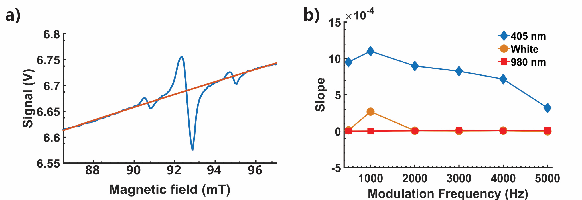
Figure 9(a) shows the raw EDMR data, illustrating the presence of a linear baseline. In order to correct for this, we fit the baseline of the measured spectra with a first order polynomial equation and subtracted this from the data, resulting in the flat baselines seen in Figures 2 and 3. Figure 9(a) also shows the fit used for the baseline correction.
Figure 9(b) shows the slopes of the linear fits obtained as a function of modulation frequency for each of the three optical excitation schemes, showing that the baseline correction did not significantly interfere with our analysis. For the 405 nm laser signal, the slope of the linear fit shows a similar trend when compared to the signal intensity. However, no such dependence is observed for the white light source and the 980 nm excitation. We currently do not know the origin of the baseline signal. However one possible explanation is that this slope is related to the magneto-resistance discovered in lightly doped phosphorus silicon Porter and Marrows (2012).
The signal intensity in the main manuscript is calculated from the resonance peak area after base line correction. The experimental spectra are scaled by lock-in amplifier and current preamplifier settings. The error bars shown in Figures 5 and 6 were calculated using the standard deviation of the baseline (following subtraction of the linear fit).
Appendix E Spectral Fits for Modulation and Power Dependence
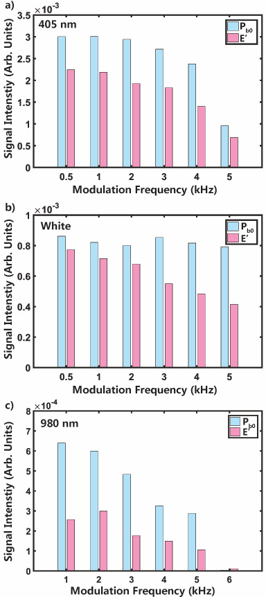
We performed two-component fits for the defect spectra measured under different modulation frequency and microwave power excitations. The modulation frequency dependence is shown in Figure 10, while the microwave power dependence is shown in Figure 11. The modulation frequency dependence of both components is similar to that of the total signal for the monochromatic excitations at 405 nm and 980 nm. With white light excitation, it appears that the main modulation dependence arises from E’ defects. The microwave power dependence of the two components follows the overall signal at 405 nm, but at 980 nm it appears that the defect signal is independent of microwave power. As noted earlier, care should be taken in interpreting these results as some of the defect signal also arises from E’-Pb0 pairs, which results in correlated signals.
