Implementing robust neuromodulation in neuromorphic circuits
Abstract
We introduce a methodology to implement the physiological transition between distinct neuronal spiking modes in electronic circuits composed of resistors, capacitors and transistors. The result is a simple neuromorphic device organized by the same geometry and exhibiting the same input–output properties as high-dimensional electrophysiological neuron models. Preliminary experimental results highlight the robustness of the approach in real-world applications.
I Introduction
Nature offers spectacular examples of energy-efficient, lightweight control architectures. Flight control in an animal like a honeybee outperforms the latest robotic architectures in terms of energy consumption, adaptability, robustness, and dimensions. Neuromorphic engineering aims at emulating the way in which biological neuronal systems perceive and represent the outside world, take decisions and develop computations, and command motor outputs [1, 2].
In implementing the dynamical behavior of biological neurons in electronic hardware we face the compromise between fidelity of the reproduced behavior and complexity of the designed circuit. Existing silicon neuron designs span a variety of solutions: from detailed implementation of neuron biophysics [3] to implementation of simple, abstract neuron models [4]. Both approaches have advantages and disadvantages, and it is an active research area to determine which implementation to use depending on the desired objective [5].
The possibility of robustly and rapidly switching between distinct activity modes is one of the peculiarity of biological neurons, which allows them to adapt their input–output response to internal and environmental conditions. Two fundamental neuronal activity modes are tonic spiking and bursting. Tonic spiking describes the slow, regular generation of spikes in the neuron membrane potential. Bursting describes the alternation between moments of low membrane potential and moments of high oscillatory activity, in which spikes are generated at very high frequency. The transition between tonic spiking and bursting plays a major role in neuronal information processing by modulating neuron input–output behavior [6, 7, 8].
We showed [9, 10] that all biological neurons share the same geometry at the transition between distinct spiking modes. In particular, this transition can be described in a simple, abstract model given by the normal form of an organizing singularity. Roughly speaking, a singularity describes a highly degenerate and fragile situation that correspond to the transition between distinct regimes [11]. There is a direct correspondence between biophysical parameters and mathematical parameters in the abstract model, which leads to a novel mathematical understanding of robustness and modulation of neuronal activity [12]. We further showed that the same qualitative picture can be realized in simple input–output circuits [13].
In this paper we follow the recipe provided in [13] to design a neuromorphic circuit with the property of exhibiting the same qualitative geometry, robustness, modulation capabilities, and input–output behavior as biophysical neuron models. As a first, biologically relevant illustration, we focus on the transition between tonic spiking and bursting. The resulting circuit solely uses six transistors and passive elements and its robust real-world implementation in low-cost components solely uses four additional transistors to overcome loading effects.
The key contributions with respect to existing neuromorphic design methods [5, 14, 15] are threefold. First, the equivalence (from a geometric, dynamical systems, and input–output perspective) of the designed circuit and high-dimensional biophysical neuron models close to the transition between distinct spiking modes is a provable consequence of the used approach. Second, the geometric nature of our methodology avoids laborious and non-constructive parameter fitting procedures, and, third, it also ensures robustness to components variability in real-world applications.
In Section II we rapidly review the results in [9, 10, 13]. Grounded in these works, we derive an implementation of our neuromorphic device in Section III and simulate it in ngspice [16] (the code can be found in the Appendix). The actual implementation of this circuit and preliminary experimental tests are reported in Section IV. Future directions are discussed in Section V.
II The geometry of neuronal behaviors and its block realization
Electrophysiological models of neurons are constructed upon the seminal work of Hodgkin and Huxley [17]. They all share the physical interpretation of the nonlinear RC circuit depicted in Fig. 1-A. The capacitor models the neuron lipidic membrane and the other branches, containing a voltage source and a variable resistance, model the flow of a specific ion across the membrane.
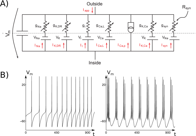
Ion flow across the membrane is dynamically regulated by the membrane potential via opening and closing of ion channels, which makes the circuit in Fig. 1-A highly nonlinear. As such, it can exhibit a rich variety of dynamical behaviors. The present paper focuses on two fundamentals behaviors shared by almost all neuron types: the tonic spiking behavior of Fig. 1-B left and the bursting behavior of Fig. 1-B right.
Reproducing tonic spiking and bursting, as well as the transition between these two modes, in an electrophysiological model requires an empirical tuning of the many biophysical parameters that usually ends up in an extensive brute-force computational parameter search [19]. A different approach relies on bifurcation theory [20].
Roughly speaking, bifurcation theory makes the ansatz that the vector field associated to an electrophysiological model undergoes some qualitative change at the transition between two distinct activity modes.
We showed in [9, 10] that the bifurcation associated to the transition between tonic spiking and bursting can be algebraically tracked by exploiting the multi-timescale nature of electrophysiological neuron models and by detecting a transcritical singularity in the critical manifold of the associated singularly perturbed dynamics. We refer the reader to [21] for an introduction to geometric singular perturbation theory and to [11] for singularity theory concepts.
The power of this analysis is that we can visualize the geometry of the tonic spiking–bursting transition in a low-dimensional normal form of the organizing singularity:
| (1a) | ||||
| (1b) | ||||
| (1c) | ||||
where is called the bifurcation parameter, are called unfolding parameters, and model timescale separation between the three state variables , and . The system is driven by the external input . The distinction between bifurcation and unfolding parameters is instrumental to the tools used in the construction of the normal form (1), that is, singularity theory applied to bifurcation problems [11].
The main theorem in [10] provides constructive conditions on the parameters in model (1) to enforce the existence of a bursting attractor. This attractor exists for parameters close to the same transcritical singularity organizing the transition between tonic spiking and bursting in biophysical conductance-based models. As a corollary, the results in [10] therefore provide a geometric way of exploring the transition between bursting and tonic spiking.
Fig. 2-A shows the temporal traces and the projection onto the phase plane of the slow–fast subsystem (1a)-(1b) of tonic spiking and bursting behaviors in model (1). Due to timescale separation, trajectories spend most of the time near the critical manifold
| (2) |
that is, the -nullcline composed of steady states as and vary.
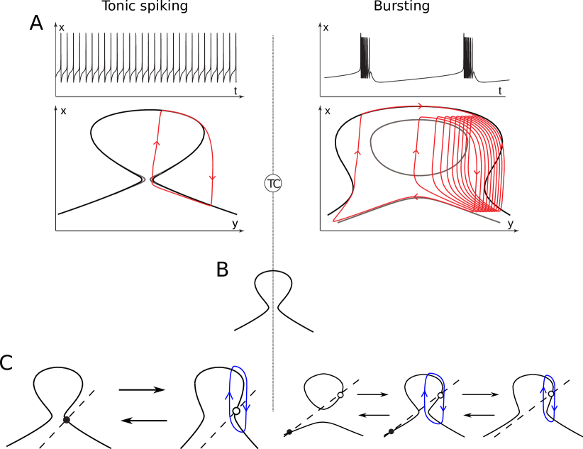
The fundamental geometric shape underlying the transition between tonic spiking and bursting is the mirrored hysteresis bifurcation diagram introduced in [10] and sketched in Fig. 2-B. In the tonic spiking mode, trajectories solely visit the right branch of the mirrored hysteresis organizing the critical manifold, whereas in bursting mode trajectories alternate between the two branches.
The geometry of both behaviors is summarized in Fig. 2-C. In tonic mode, for a fixed value of the ultra-slow variable , the slow–fast subsystem possesses a single attractor on the right branch of the mirrored hysteresis: either a stable fixed point, for a large value of (left plot), or a stable limit cycle, for a small value of (right plot). For large initial values of the model is therefore at quasi-steady state. In this case the ultra-slow dynamics (1c) forces to decrease until the steady state looses stability and a spike is emitted along the newborn limit cycle. This in turn leads to a sharp increase of , which immediately lets the steady state recover stability, and the model is forced back to quasi-steady state after a single spike.
In bursting mode, there exists a large range of values of the ultra-slow variable in which the slow–fast subsystem exhibits bistability between a stable steady state on the left branch of the mirrored hysteresis and a limit cycle on the right branch of the mirrored hysteresis (center plot). Bursting arises from ultra-slow hysteretic evolution around this bistable region.
For a large initial value of the sole attractor is a stable steady state (left plot). The ultra-slow dynamics (1c) forces to decrease. However, once in the bistable region, the model remains at quasi-steady state. Only for sufficiently small the steady state looses stability and the trajectory converges toward the spiking limit cycle, which is now the sole attractor (left plot). On the limit cycle the ultra-slow dynamics (1c) forces to increase. Again, all through the bistable region the system remains in the oscillatory mode and only for sufficiently large the trajectory converges back to the quasi-steady state.
Normal forms are useful not only because they unmask the geometry underlying a given dynamical behavior, but also because they possess the minimum number of parameters to reproduce a family of behaviors of interest. As such they can also be implemented in physical devices more easily and robustly than the original biophysical model, yet, preserving the same geometric and input–output properties.
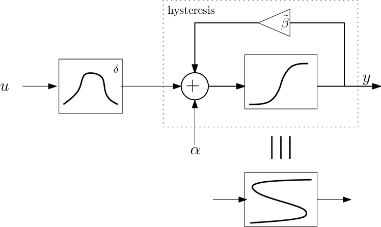
We showed in [13] that the mirrored hysteresis bifurcation diagram at the core of model (1) can be realized in the input–output diagram of Fig. 3. Its basic ingredients are a non-monotone nonlinearity cascaded with a saturation nonlinearity and a positive feedback loop around the saturation nonlinearity. The positive feedback loop transforms the saturation into a hysteresis [13, Proposition 1], the non-monotone block creates a mirror of the resulting hysteretic characteristic.
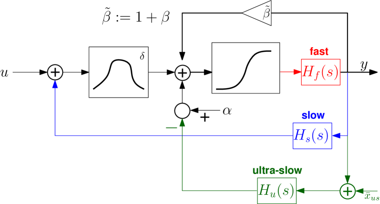
Adding linear dynamical systems evolving on three sharply different timescales (Fig. 4) transforms the static diagram in Fig. 3 into a three-timescale dynamical system with the same qualitative behavior of model (1). In particular, the diagram in Fig. 4 exhibits the same geometric transition between tonic spiking and bursting as model (1) [13, Theorem 3].
III Electronic implementation

In this section we derive an electronic implementation of the diagram in Fig. 4. The main active component is an NPN transistor. Its constitutive relations are given by Ebers-Moll equations [22] but, to simplify the analysis, we will model the transistor as a current source with current proportional to that of a diode standing at the base (see Fig. 5). Furthermore, we regard the diode as a perfect switch that opens whenever the base–emitter voltage is lower or equal to 0.6 V, and closes otherwise. Also, the minimal voltage between the collector and the emitter is equal to 0.1 V, a point at which the proportional relation among the base and emitter currents is lost.
III-A Non-smooth analysis
The simplified transistor description leads to piecewise linear models that are easily dealt with using non-smooth analysis. To make the paper self contained, we recall some definitions and results. See [23, 24] for further details.
Definition 1
[24, p. 27] Consider a function with a Banach space. The generalized directional derivative of at in the direction of , denoted , is defined as
The generalized gradient of at , denoted , is a subset of the dual space given by
Here we will set and identify with its dual, so is taken as a subset of . In this case we have:
Theorem 1
[24, p. 63] Let be Lipschitz near and let be the set of points at which fails to be differentiable. Suppose that is any set of Lebesgue measure 0 in . Then,
Theorem 2
[23, p. 38] If is locally Lipschitz at and attains its extremum at , then
The smooth version of the implicit function theorem is a common tool for finding singular points in classical bifurcation theory. Let us present a non-smooth version for non-smooth problems. Consider a Lipschitz function together with the equation
| (3) |
Suppose there is a pair that solves (3) and
where is the generalized gradient with respect to . The implicit function theorem [24, p. 256] states that there exists a neighborhood of and a Lipschitz function such that and such that, for every ,
III-B Voltage-controlled non-monotone characteristic
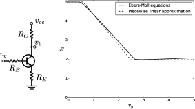
The non-monotone block of the circuit in Fig. 4 is realized as the difference of two monotone nonlinearities [13]. A common emitter NPN transistor configuration serves as a simple, natural saturation monotone nonlinearity (see Fig. 6). In view of the transistor model described above, the – characteristic takes the piecewise linear form
| (4) |
where is the voltage at the power source,
is the voltage gain (the slope of the saturation), is the transistor’s current gain and with
the saturation voltage. Usually, one chooses so that , that is, so that the dependence of on is negligible.
is the operator that projects its argument into the set , that is,
For our particular , the projection translates into
The projection captures the fact that the diode does not conduct when is below 0.6 V and that saturates when reaches 0.1 V. To asses the quality of our estimation, we choose a set of parameters and compare (4) against the simulation obtained using ngspice (which implements Ebers-Moll equations). The results are shown in Fig. 6.
The parallel interconnection achieving the non-monotone behavior is shown in Fig. 7, left. Applying Kirchhoff’s laws and the piecewise linear model for the transistor one obtains
| (5) |
with
(see Fig. 7, right).
The characteristic (5) is non-monotone whenever strict extrema are present. Recall that a necessary condition for the presence of extrema is , where is the generalized gradient of with respect to . Note that
| (6) |
with and the interior and the boundary of , respectively. Application of the chain rule to (5) gives
A necessary condition for is
| (7) |
This inequality imposes a set of conditions to be satisfied by the resistors , , , , and .
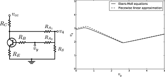
When inequality (7) holds strictly (the equality does not happen in practice), the inclusion occurs at the boundary of , that is, at the points that satisfy
We thus have the following points of interest for (5):
The computation of such points is again useful for choosing the appropriate resistors. The objective is to have the minimum occur as close as possible to , and to have the largest possible excursion along the axis.
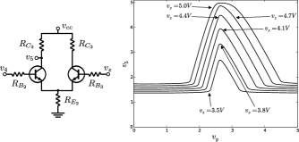
In the block realization in Fig. 4, the output of the non-monotone block is modulated by the unfolding parameter . Such modulation is necessary to transition along the three possible characteristics in Fig. 2-C. The same modulation is achieved here by cascading a differential amplifier with the non-monotone characteristic. In this way, an external voltage can be used to the scale the input–output characteristic, as shown in Fig. 8, left. We have
with . The currents are thus
with
Let and . When does not saturate, i.e., when
the output voltage is
| (8) |
where
and the interval is determined by
The voltage is called the non-inverting input and the inverting one. The complete block is shown in Fig. 10 and the input–output characteristic is shown in Fig. 8, right.
III-C Hysteretic characteristic

The hysteretic block is built as the positive feedback of a basic saturation and a linear gain [13]. This is achieved at once with another differential amplifier. By letting be the inverting input, the non-inverting input and the output, we obtain, cf. (8),
Positive feedback is then achieved simply by setting , as shown in Fig. 9. This results in the piecewise linear characteristic
| (9) |
It follows from the implicit function theorem that a necessary condition for the existence of singular points is , with the generalized gradient taken with respect to . Application of the chain rule to (9) gives
A necessary condition for is thus . There are two points of singularity occurring at the boundary of . The first one is characterized by
which, together with the condition , gives
The other point of singularity is determined by
which gives
(see Fig. 9). For this block, the resistors were chosen so that the first and second singularities occur, respectively, at one and two thirds of the chosen voltage range of 5 V.
III-D Voltage-controlled mirrored hysteresis

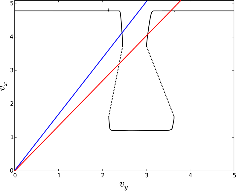
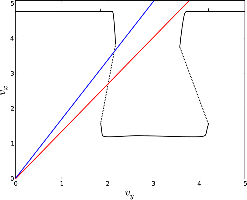
The cascade of the voltage-controlled non-monotone block and the hysteresis is shown in Fig. 10. This interconnection realizes the block diagram in Fig. 3. The circuit establishes the desired static behavior relating , and , that is, it implements a voltage characteristic that is topologically equivalent to the algebraic variety given by (2). In other words, it produces the desired voltage-controlled mirror hysteresis (see Figs. 11, black traces). Compared to Figs. 2-C, the simulated responses are, on one hand, stiffer and, on the other, reflected along a horizontal axis. However, this does not alter the qualitative picture in terms of number and type of different possible attractors. In this sense we say that the two portraits are qualitatively equivalent.

III-E Burster
We now transform the static circuit in Fig. 10 into a dynamic circuit exhibiting the same qualitative dynamics as model (1). The parasitic capacitances of the transistors provide the fast dynamics and set its corresponding timescale (cf. in Fig. 4). The voltage is fed back to by means of a resistive voltage divider and a capacitor. The values of the resistors and the capacitor determine the timescale of the slow dynamics as well as the slope of its nullcline (cf. in Fig. 4). For bursting, we choose the resistors in such a way that this slope is small and the nullcline intersects both branches of the mirrored hysteresis, as in Fig. 2.
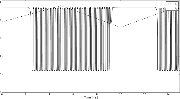
Fig. 11 confirms the qualitative equivalence of the circuit in Fig. 10 and model (1). By sweeping we recover the same qualitative phase portraits of Fig. 2-C left, which underlie the behavior simulated in Fig. 12. A key ingredient in the bursting behavior is the bistability of the limit cycle and the node (Fig. 11(b), red). The presence of this phenomenon can be asserted by noting that the transition from the constant output (the stable node) to the oscillating behavior (the limit cycle) occurs at a higher value of than the one for the transition from the oscillating behavior back to the constant output.
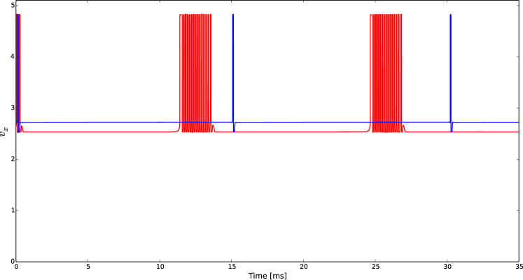
Bursting is finally achieved by feeding back to through the ultra slow filter . This is again realized with a voltage divider and a capacitor, but now the circuit’s time-constant is chosen much larger. To ensure a robust operation, the output of is amplified so that exhibits a large swing. In fact it is the complement of that is passed through an amplifier with negative slope (this accounts for the sixth transistor). The complete circuit is shown in Fig. 14 and its time response is shown in Fig. 13.
III-F Spiker
Recall that the mirrored hysteresis captures both modes of operation: bursting and tonic spiking. Geometrically, the difference between the two behaviors is the locus of the stable fixed point, as sketched in Fig. 2. In our circuit, we recover the same geometric picture by changing the slope of the -nullcline via tuning of the resistance and . When the slope of the nullcline is sufficiently large this line solely intersects the left branch of the mirrored hysteresis at the transition between spiking and resting (see Figs. 11(b) and 11(c), blue), thus destroying the possibility of the bistability underlying bursting. The model is in this case in the tonic spiking mode shown in Fig. 13.

All the results of this section can be easily reproduced using the code provided in the appendix.
III-G Modulation of excitability properties in electronic devices
The possibility of reliably switching between bursting and tonic spiking is relevant because it provides a means to modulate the input–output behavior of our circuit. The output is the fast capacitor voltage . We introduce inputs by adding a current source at the node labeled in Fig. 14. The injected current corresponds to in (1). Sufficiently large positive applied currents set the circuit in a stable resting state, both in the tonic and bursting modes. The resting state is however excitable: the response to excitatory (that is, negative for our circuit) input is large and highly nonlinear (spiking), reflecting the latent nonlinear dynamics of the circuit (Fig. 15).
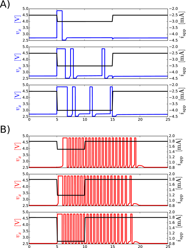
Excitability is sharply different in tonic and bursting modes [7]. The tonic mode is characterized by a quasi-linear coding of incoming inputs: the response of the circuit lasts only as long as the excitatory input is applied and the elicited spiking frequency is roughly proportional to the magnitude of the excitatory inputs. On the contrary, the bursting mode is characterized by a nonlinear detection mechanism of incoming inputs: the response of the circuit lasts for a fixed amount of time that can outlast the length of the excitatory stimuli (memory) and the elicited frequency is roughly independent of the input magnitude. Excitability in bursting mode serves as a bell ring signaling the arrival of new incoming inputs (for instance an unexpected sensory stimulus), whereas excitability in tonic mode serves as a frequency-coding mechanism to transmit information about those inputs. The possibility of switching between the two modes is widespread in the brain [7, 8].
Our circuit exhibits the same behavioral transition. In the tonic mode the voltage output response roughly codifies the input current step magnitude (Fig. 15A). In the bursting mode it responds with bursts whose length and interspike frequency are virtually independent of the magnitude of the input current (Fig. 15B).
IV Real-world implementation
The real circuit was built using the same methodology used for designing the simulated circuit. First, a non-monotone block was built as in Section III-B. Using the formulas in that section, the resistors were tuned so that the local minimum occurs at half the voltage range, . The output of the non-monotone block was connected to a differential amplifier without much difference with the simulated design. A hysteretic characteristic was implemented by means of a differential amplifier in positive feedback. Again, the resistors were chosen in order to have have a symmetric characteristic with a large swing in . The direct interconnection of the voltage-controlled block and the hysteresis did not work as expected, the main reason being the fact that the hysteretical block draws a non-negligible current from the non-monotone block and changes its behavior (a phenomenon usually referred to as loading). To overcome this issue, an extra transistor in an emitter-follower configuration was inserted between these two blocks. In this configuration, the extra transistor presents high input and low output impedances, allowing the hysteretical block to be driven by the non-monotone block, but preventing the hysteretical block from affecting the behavior of the non-monotone block. This effectively overcomes the loading problem and simplifies the tuning of the circuit parameters, but induces a stiffer characteristic.

The resulting circuit is depicted on the upper half of the circuit shown in Fig. 16. The voltage-controlled non-monotone block is composed of transistors Q1-Q3, the emitter-follower transistor corresponds to Q4 and the hysteretical block is formed by transistors Q5-Q6. The behaviour is shown in Fig. 17. It can be seen that the responses are indeed stiffer than the simulated ones, but remain qualitatively equivalent to the mirrored hysteresis of Figs. 2-C.
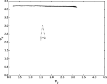
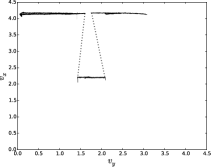
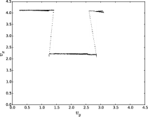
The – feedback loop is closed by means of another transistor in a common-emitter configuration, Q7, with a response similar to the one depicted in Fig. 6. The negative slope presented by this block is corrected by taking the complementary output of at the collector of Q6, instead of itself at the collector of Q5. The 11 nF ceramic capacitor and the 100 k potentiometer set the slow time-scale. The potentiometer also permits to adjust the slope of the -nullcline in a similar way as in Fig. 11. Indeed, by properly adjusting the potentiometer, it is possible to set the circuit either in bursting or in tonic spiking mode.
Closing the – loop is slightly more complicated. First, an emitter-follower, Q8, is used for the same impedance-matching purposes as before. A 10 F electrolytic capacitor and a 5.6 k resistor set the ultra slow time-scale. The output of the ultra slow filter is then connected to a two-stage amplifier, Q9-Q10, that works as a signal conditioner which translates the voltage change in that arises when transitioning from the upper stable equilibrium (4 V) to the stable limit cycle (3 V, average), into the voltage change required in for transitioning between the mirrored hysteresis of Fig. 17(c) (2.7 V) and Fig. 17(a) (0.8 V). The desired bursting and tonic spiking modes are finally shown in Fig. 18. As explained above, it is possible to smoothly transition from one mode to the other simply by adjusting the 100 k potentiometer.
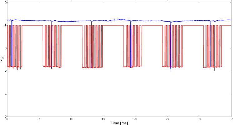
It is worth mentioning that the circuit was built using common low-cost components. All the transistors have part number 2N2222. The resistors have precision tolerances of 5 %, while the capacitors have precision tolerances of 10 %. The low precision of the components attests to the intrinsic robust nature of the singularity approach. To further asses the robustness of the design, the transistors where randomly swapped. The resulting responses were virtually indistinguishable.
V Conclusion and perspectives
V-A A robust geometric neuromorphic circuit design methodology
Instead of relying on fine, non-constructive parameter tuning, the design methodology introduced in this paper allows to implement desired behaviors in electronic circuits from the geometrical inspection of the static characteristic of suitable sub-circuits. The proposed methodology is a direct application of the geometric analysis of neuronal behaviors in [9, 10] and of the realization theory in [13]. The main extension was the use of non-smooth analysis to cope with the switching behavior typical of electronic devices. When applied to the biological transition between tonic spiking and bursting the result of the proposed methodology is a compact six-transistor ngspice model that only requires four additional transistors for a robust, low-cost component, real-world implementation.
V-B Reliable excitability modulation in neuromorphic circuits
Because the same geometry of high-dimensional neuron models is being enforced, it is natural to expect that the proposed methodology enforces the same input–output behavior. The transition between tonic spiking and bursting is associated with a switch in excitability type from linear input coding to nonlinear input detection that plays a fundamental role in brain functions. The same qualitative transition is reliably reproduced in the designed neuromorphic devices. Other excitability transitions could robustly and efficiently be implemented following the same geometric methodology, which provides the main advantage with respect to available neuromorphic circuit design methods.
V-C Perspective
The possibility of implementing the transition between distinct excitability types in simple, inexpensive, and robust neuromorphic circuits opens the path, for instance, to the design of neuromorphic sensors inspired by the thalamus, the main sensory hub in the central nervous system, where this transition plays a major role in the efficient coding of sensory stimuli [7].
In terms of computational capabilities, spike-based neural networks offer several promising features such as selective attention [25] and homeostasis [26].
More generally, because virtually any higher-level brain function relies on the modulation of spiking and the excitability property at the single neuron level [8], the designed circuit potentially provides a novel building block for any neuromorphic circuit in which neuromodulation is essential.
Acknowledgments
Alessio Franci acknowledges support by DGAPA-PAPIIT (UNAM) grant IA105816.
References
- [1] K. Boahen, “Neuromorphic microchips,” Scientific American, vol. 292, no. 5, pp. 56–63, 2005.
- [2] S.-C. Liu and T. Delbruck, “Neuromorphic sensory systems,” Current opinion in neurobiology, vol. 20, no. 3, pp. 288–295, 2010.
- [3] K. M. Hynna and K. Boahen, “Thermodynamically equivalent silicon models of voltage-dependent ion channels,” Neural Computation, vol. 19, no. 2, pp. 327–350, 2007.
- [4] J. H. Wijekoon and P. Dudek, “Compact silicon neuron circuit with spiking and bursting behaviour,” Neural Networks, vol. 21, no. 2, pp. 524–534, 2008.
- [5] G. Indiveri, B. Linares-Barranco, T. J. Hamilton, A. Van Schaik, R. Etienne-Cummings, T. Delbruck, S.-C. Liu, P. Dudek, P. Häfliger, S. Renaud et al., “Neuromorphic silicon neuron circuits,” Frontiers in neuroscience, vol. 5, 2011.
- [6] R. Krahe and F. Gabbiani, “Burst firing in sensory systems,” Nature Reviews Neuroscience, vol. 5, no. 1, pp. 13–23, 2004.
- [7] S. S. Sherman and R. W. Guillery, Exploring the thalamus. Oxford Univ Press, 2001, vol. 312.
- [8] S.-H. Lee and Y. Dan, “Neuromodulation of brain states,” Neuron, vol. 76, no. 1, pp. 209–222, 2012.
- [9] A. Franci, G. Drion, V. Seutin, and R. Sepulchre, “A balance equation determines a switch in neuronal excitability,” PLoS Computational Biology, 2013.
- [10] A. Franci, G. Drion, and R. Sepulchre, “Modeling the modulation of neuronal bursting: a singularity theory approach,” SIAM Journal on Applied Dynamical Systems, vol. 13, no. 2, pp. 798–829, 2014.
- [11] D. G. Schaeffer and M. Golubitsky, “Singularities and groups in bifurcation theory,” Appl. Math. Sci, vol. 51, 1985.
- [12] G. Drion, A. Franci, J. Dethier, and R. Sepulchre, “Dynamic input conductances shape neuronal spiking,” eneuro, vol. 2, no. 2, pp. ENEURO–0031, 2015.
- [13] A. Franci and R. Sepulchre, “Realization of nonlinear behaviors from organizing centers,” in Proc. Conference on Decision and Control, Los Angeles, CA, Dec. 2014, pp. 56 – 61.
- [14] J. Misra and I. Saha, “Artificial neural networks in hardware: A survey of two decades of progress,” Neurocomputing, vol. 74, pp. 239 – 255, Dec. 2010.
- [15] A.-D. Almási, S. Woźniak, V. Cristea, Y. Leblebici, and T. Engbersen, “Review of advances in neural networks: Neural design technology stack,” Neurocomputing, vol. 174 A, pp. 31 – 41, Jan. 2016.
- [16] Ngspice. [Online]. Available: http://ngspice.sourceforge.net/
- [17] A. L. Hodgkin and A. F. Huxley, “A quantitative description of membrane current and its application to conduction and excitation in nerve,” The Journal of physiology, vol. 117, no. 4, pp. 500–544, 1952.
- [18] G. Drion, L. Massotte, R. Sepulchre, and V. Seutin, “How modeling can reconcile apparently discrepant experimental results: the case of pacemaking in dopaminergic neurons,” PLoS Comput Biol, vol. 7, no. 5, pp. e1 002 050–e1 002 050, 2011.
- [19] A. A. Prinz, C. P. Billimoria, and E. Marder, “Alternative to hand-tuning conductance-based models: construction and analysis of databases of model neurons,” Journal of Neurophysiology, vol. 90, no. 6, pp. 3998–4015, 2003.
- [20] J. Guckenheimer and P. Holmes, Nonlinear oscillations, dynamical systems, and bifurcations of vector fields. Springer Science & Business Media, 1983, vol. 42.
- [21] C. K. R. T. Jones, “Geometric singular perturbation theory,” in Dynamical systems. Springer, 1995, pp. 44–118.
- [22] A. S. Sedra and K. C. Smith, Microelectronic Circuits. New York: Oxford University Press, 2004.
- [23] M. M. Mäkelä and P. Neittaanmäki, Nonsmooth optimization. Singapore: World Scientific, 1992.
- [24] F. H. Clarke, Optimization and Nonsmooth Analisis. New York: Society for Industrial and Applied Mathematics, 1990.
- [25] C. Bartolozzi and G. Indiverti, “Selective attention implemented with dynamic synapses and integrate-and-fire neurons,” Neurocomputing, vol. 69, pp. 1971 – 1976, Oct. 2006.
- [26] ——, “Global scaling of synaptic efficacy: Homeostasis in silicon synapses,” Neurocomputing, vol. 72, pp. 726 – 731, Jan. 2009.
Simulations were carried using ngspice. The circuit simulator is a well-documented open-source implementation of Spice3, Cider and Xspice. The following code describes the circuit depicted in Fig. 14 and was used to produce the plots shown in Fig. 13.
* this is complete.cir file * voltage resources vcc 5 0 dc 5V * non monotone q1 2 3 4 2n2222bis rC1 5 2 16k rB1 3 1 100k rE1 4 0 10k Ra1 6 1 100k Ra2 6 2 33k Rs 6 0 220k * non monotone modulation q2 7 8 9 2n2222bis q3 10 11 9 2n2222bis rC2 7 5 4.7k rC3 10 5 4.7k rB2 8 6 1k rB3 12 11 1.2k rE2 9 0 470 * hysteresis q4 13 14 15 2n2222bis q5 16 17 15 2n2222bis rC4 13 5 820 rC5 16 5 240 rB4 14 7 2.4k rB5 17 13 6k rE4 15 0 240 * vy-vx feedback loop ri1 13 1 15k ri2 1 0 47k * Set ri2 to 34.5k for tonic spiking ciF 1 0 22n * vz-vx feedback loop q6 12 18 19 2n2222bis ro1 16 18 4.7k ro2 18 0 4.7k coF 18 0 4.7u rC6 12 5 200 rE6 19 0 20 rbi 19 5 150 * model for a 2n2222 transistor .model 2n2222bis npn (is=14.34f bf=255.9 + vaf=74.03 ikf=.2847 ise=14.34f ne=1.307 + br=6.092 ikr=0 isc=0 nc=2 rb=10 rc=1 + cje=22.01p tf=411.1p cjc=7.306p tr=46.91n + xtb=1.5 Xti=3 Eg=1.11 Mjc=.3416 Vjc=.75 + Fc=.5 Mje=.377 Vje=.75 Itf=.6 Vtf=1.7 + Xtf=3 ) .control tran 1us 40ms plot v(16) ylimit 0 5 .endc .end