Influence of excitonic effects on luminescence quantum yield in silicon
Abstract
Nonradiative exciton lifetime in silicon is determined by comparison of the experimental and theoretical curves of bulk minority charge carriers lifetime on doping and excitation levels. This value is used to analyze the influence of excitonic effects on internal luminescence quantum yield at room temperature, taking into account both nonradiative and radiative exciton lifetimes. A range of Shockley-Hall-Reed lifetimes is found, where excitonic effects lead to an increase of internal luminescence quantum yield.
Keywords: silicon, excitons, luminescence, quantum yield, recombination
I Introduction
Excitonic effects in both radiative and nonradiative recombination play an important role in photo- and electroluminescence processes, whose quantum yield is about 10% and 1%, respectively Green01 ; Ng01 . Their influence on the photoelectric processes in silicon-based devices, such as solar cells, was studied in a number of publications Kane93 ; Corkish93 ; Green98 ; Gorban00 .
Investigations of bulk lifetime in silicon as a function of doping and excitation levels were initiated by Hangleiter Hangleiter88 , who considered the spatial correlation of two electrons and a hole (or two holes and an electron), which exists in the presence of an exciton. This correlation leads to an increased probability of Auger recombination, in which the energy released is transferred to another charge carrier. It can proceed both via the interband and the deep impurity mechanisms.
Excitons’ effect on electoluminescence in silicon were considered in Sachenko06 . However, the effect of nonradiative exciton recombination in n-type silicon was overestimated in that work.
Here, a more accurate value of exciton nonradiative lifetime is obtained by means of comparison between the theoretical and experimental dependences of the bulk lifetime on doping and excitation levels in silicon. In this comparison, improved theoretical expressions for the interband Auger recombination rate from Ref. Richter12, are used. The so obtained lifetime served as an input parameter to analyze the contribution of excitonic effects to the luminescence internal quantum yield in silicon. Both the positive effect of radiative exciton recombination and the negative effect of nonradiative recombination are taken into account. Quantum yield dependence on doping and excitation levels, as well as the influence of surface recombination on quantum yield at room temperature are analyzed. It is shown that, at Shockley-Hall-Reed lifetime exceeding 1 ms, radiative exciton recombination dominates; in the opposite case, the negative, i.e., nonradiative effect takes over.
II Nonradiative exciton lifetime in silicon
As shown in Ref. Sachenko00, based on the results obtained by Hangleiter Hangleiter88 , the presence of the exciton subsystem in silicon at sufficiently high doping and excitation levels leads to an onset of the nonradiative exciton recombination channel via Auger mechanism on deep impurities. Its characteristic time is
| (1) |
where is Shockley-Reed-Hall lifetime, is the density of electron-hole pairs, consisting of the equilibrium, , and excess, , contributions, and is the parameter of the theory. In the case considered here, practically coincides with the doping level. On the other hand, the non-radiative recombination rate can be written as Sachenko00
| (2) |
where is the density of recombination (trap) centers, the probability of Auger recombination on an impurity,
| (3) |
being the exciton Bohr radius, the binding energy of the exciton ground state, and , , and the effective densities of states in the conduction, valence, and exciton bands in silicon. Combination of Eqs. (1) and (2), taking into account that , where is the capture coefficient of a minority carrier by a deep impurity, gives
| (4) |
Taking meV, nm, cm-3, cm-3, cm-3, K, and assuming that the electron density is well below the Mott transition threshold (about cm-3), we obtain cm-3 and cm-3 Kane93 .
As this estimate shows, the ratio in silicon is of the order of unity. This means that is of the same order of magnitude as the ratio of the capture coefficient by a deep impurity level to the probability of impurity-assisted Auger recombination.
In the work Sachenko00, , the value of cm-3 was determined by analyzing the experimental data for the inverse effective lifetime, vs. doping level in silicon, published in the literature. There are reasons to believe that this figure underestimates the true value of , because, as will be shown below, it does not agree well with the experimental results published in those works, where the surface recombination rate was minimized to such a degree that its influence on was negligible. In this case, the effective recombination rate is determined by the Shockley-Hall-Reed recombination, nonradiative exciton recombination, radiative band-to-band and exciton recombination, and interband Auger recombination rates:
| (5) |
Here, is the interband recombination lifetime with the respective parameter , is the radiative exciton recombination lifetime with the parameter , see Ref. Sachenko06, , and is the interband Auger recombination lifetime given by an empirical expression (18) from Ref. Richter12, .
For further treatment, we need to specify the parameters in Eqs. (1)-(5). We will treat the Shockley-Hall-Reed lifetime as an adjustable parameter. Let us focus on the room-temperature case. Then, at low doping levels, the recombination parameters are Sachenko06 cm-3/s and cm-3/s. As the doping level increases, the electron-hole interaction becomes screened, leading to the reduction of . To account for this effect, has to be multiplied by a factor , see Ref. Sachenko00-1, .
In order to find , we use the experimental dependence of on reported in Refs. Richter12, ; Fossum76, ; Hacker94, ; Beck73, ; Passari83, , and also the improved empirical formula for obtained in Richter12 .
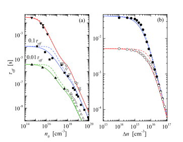
The results of comparison of the experimental curve with the theoretical one, obtained using the expressions from Ref. Richter12, , are shown in Fig. 1(a). The theoretical calculations were performed using Eq. (5), both with and without taking into account the nonradiative exciton recombination. Fig. 1(b) shows the experimental dependence of on the excitation level from Ref. Yablonovitch86, .
It should be noted that, in order to obtain an accurate estimate for from the experimental curves for , see Fig. 1, using the relation (5), the graphical accuracy is insufficient. Therefore, we first excluded the effect of the interband Auger recombination using the expressions from Ref. Richter12, (neglecting the radiative recombination). As a result, we obtained a simple expression
| (6) |
which implies that the combination
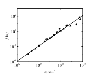
| (7) |
is a linear function of , whose slope is . Note that the function is universal, i.e. independent of . Fig. 2 shows this function, obtained theoretically and based on the experimental results of Refs. Fossum76 ; Hacker94 ; Yablonovitch86 (with interband Auger recombination taken into account). For each of the three experimental curves, was found using the least squares method, yielding in all three cases very similar values
| (8) |
It is this value that was used in all theoretical curves presented in this work.
As seen from Fig. 1, the noticeable discrepancy between the theoretical curves that do and do not take the nonradiative recombination into account occurs at , and 0.4 ms. At higher Shockley-Reed-Hall lifetimes of 30 and 40 ms, the two sets of curves are practically identical.
We note that in the work Fossum76, , a value cm-3 was obtained using the simplified expression (5), where only the first term was present in the right-hand side. However, as our analysis shows, interband Auger recombination becomes operative at doping levels higher than cm-3, which was not taken into account in Ref. Fossum76, . Therefore, quadratic exciton nonradiative recombination plays a smaller role, and the parameter has a somewhat higher value.
We note that, according to (3), the obtained value cm-3 is realized when the ratio cm-3. The independence of on the parameters of concrete deep centers can be explained by the fact that, on the one hand, responsible for the generation-recombination processes in silicon are the levels with high capture cross-section, whose energies are close to the middle of the bandgap. On the other hand, according to Ref. Haug81, , depends only weakly on the specifics of the deep levels, but is determined by their energies. Therefore, for the impurity levels, whose energy is close to the middle of the bandgap, the value of can be practically the same.
III Exciton effect on the internal luminescence quantum yield in silicon
We now apply the corrected value (8) to analyze the influence of the excitonic effects on the internal luminescence quantum yield in silicon, which can be written as
| (9) |
where is the semiconductor slab thickness, and the total recombination velocity on its both surfaces.
For simplicity, we consider the case, where the electron-hole pair diffusion length is large: . We will use the expression (5) and its truncated version, in which the terms due to the radiative and nonradiative exciton recombination are omitted.
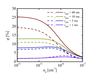
Fig. 3 shows the theoretical results for the internal luminescence quantum yield in n-type silicon. We assumed cm/s, the smallest value obtained in Ref. Yablonovitch86, . Furthermore, we took cm-3, and , and 1 ms. The solid curves are obtained taking the exciton effects into account, and the dashed ones are obtained without them.
As seen from Fig. 3, inclusion of exciton effects leads to an increase of the luminescence quantum yield when radiative exciton recombination dominates at , and 5 ms. The higher the larger luminescence quantum yield obtained taking the exciton effects into account. At ms, exciton recombination practically does not affect luminescence quantum yield at cm-3. At cm-3, the value of obtained without exciton effects is larger than with them.
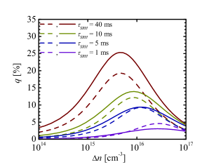
Shown in Fig. 4 are the theoretical dependence of the luminescence quantum yield on the excitation level obtained with (solid) and without (dashed) taking the exciton effects into account. As seen from this figure, all curves have a maximum. The highest value of % is realized at ms. At and 40 ms, the curves obtained with exciton effects exceed the corresponding curves obtained without taking these effects into account, at all values of . For ms, the curve obtained with the exciton effects taken into account exceeds the one without exciton effect almost everywhere, except for the region near the maximum. Finally, at ms, the two curves practically coincide for cm-3, whereas at higher , the curve obtained without exciton effects is higher.
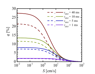
Presented in Fig. 5 is the theoretical luminescence quantum yield as a function of surface recombination velocity with and without exciton effects (solid and dashed curves, respectively). As seen in this plot, exciton effects make higher at , and 5 ms; the two curves for ms practically coincide. The higher , the smaller the surface recombination velocity, at which starts to decrease. At the typical value of of the order of cm/s, quantum yield does not exceed 0.1 %. Thus, in order to increase luminescence quantum yield, efficient methods of surface passivation are required, see Refs. Richter12, ; Yablonovitch86, for a description of such methods. In particular, it is possible to substantially reduce surface recombination velocity by using -Si:H layers of nanometer thickness Jano13 .
We note that the curves from Figs. 3-5 are obtained under the assumption that the doping level, , and the excitation level, , are independent parameters. The latter is proportional to the irradiation intensity; however, it also depends on the recombination mechanisms, including the interband Auger recombination. Therefore and are, in fact, related. This relation can be found from the generation-recombination balance equation for the photodiode silicon structures used to investigate electroluminescensce. In the open-circuit regime, and for , this equation has the form:
| (10) |
where is the short-circuit current, and is the area of the semiconductor structure.
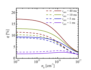
Fig. 6 shows the internal luminescence quantum yield as a function of doping level for AM1.5 conditions. As before, these curves are build with and without taking exciton effects into account (solid and dashed lines, respectively). The photocurrent density was assumed to be mA/cm2. To build these curves, we first determined from Eq. (10). Then, this dependence was substituted into Eq. (9) and into the reduced version of Eq. (9), where the recombination terms due to radiative and nonradiative exciton recombination are omitted.
As seen from Fig. 6, the curves obtained are very similar to the ones from Fig. 3. However, there is a difference between the two dependences. The main difference is that the magnitude of internal yield in Fig. 6 is smaller than in Fig. 3. This is due to the fact that the initial obtained from Eq. (7) at sufficiently small are higher than cm-3. At the same time, as seen from Fig. 4, the maximum of the curve at , and 5 ms is below cm-3. This means that, in order to increase , one needs to reduce , which is achieved by the reduction of the photogenerated current, i.e. by the reduction of the irradiation intensity. Indeed, for mA/cm2 we obtain % at ms. This agrees with the result from Fig. 3.
IV Conclusions
As shown in this work, the effective density , which determines the nonradiative exciton lifetime in silicon is cm-3. Our analysis has revealed that the exciton effects in silicon lead to an increase of the internal luminescence quantum yield at sufficiently long Shockley-Reed-Hall lifetimes exceeding 1 ms. In the opposite case, ms, this effect is absent.
Acknowledgments
M.E. is grateful to the Natural Sciences and Engineering Research Council of Canada (NSERC) and to the Research and Development Corporation of Newfoundland and Labrador (RDC) for financial support.
References
- (1) M.A. Green, J. Zhao, A. Wang, P.J. Reece, and M. Gal, Nature 412, 805 (2001).
- (2) W.L. Ng, M.A. Lourenço, R.M. Gwilliam, S. Ledain, G. Shao, and K.P. Homewood, Nature 410, 192 (2001).
- (3) D.E. Kane and R.M. Swanson, J. Appl. Phys. 73, 1193 (1993).
- (4) R. Corkish, D.S.P. Chan, and M.A. Green, J. Appl. Phys. 79, 195 (1993).
- (5) M.A. Green, in Proceedings of the 2nd World Conference and Exhibition on Photovoltaic Solar Energy Conversion, pp. 74-76 (Wien, 1998).
- (6) A.P. Gorban, A.V. Sachenko, V.P. Koslylyov, and N.A. Prima, Semicond. Phys. Quantum Electron. Optoelectron. 3, 322 (2000).
- (7) A. Hangleiter, Phys. Rev. B 37, 2594 (1988).
- (8) A.V. Sachenko, A.P. Gorban, V.P. Kostylyov, and I.O. Sokolovskyi Semiconductors 40, 884 (2006).
- (9) A. Richter, S.W. Glunz, F. Werner, J. Schmidt, and A. Cuevas, Phys. Rev. B 86, 165202 (2012).
- (10) A.V. Sachenko, A.P. Gorban, and V.P. Kostylyov, Semicond. Phys. Quantum Electron. Optoelectron. 3, 5 (2000).
- (11) A.V. Sachenko and Yu.V. Kryuchenko, Semicond. Phys. Quantum Electron. Optoelectron. 3, 150 (2000).
- (12) J.G. Fossum, Solid State Electron. 19, 269 (1976).
- (13) R. Häcker and A. Hangleiter, J. Appl. Phys. 75, 7570 (1994).
- (14) J.D. Beck and R. Conradt, Solid State Commun. 13, 93 (1973).
- (15) L. Passari and N. Susi, J. Appl. Phys. 54, 3935 (1983).
- (16) E. Yablonovitch and T. Gmitter, Appl. Phys. Lett. 49, 587 (1986).
- (17) A. Haug, Phys. Stat. Sol. B 108, 443 (1981).
- (18) A. Yano, S. Tohoda, K. Matsuyama, Y. Nakamura, T. Nishiwaki, K. Fujita, M. Taguchi, and E. Maruyama, Proceedings of the 28th European Photovoltaic Solar Energy Conference and Exhibition, p. 748 (2013).