Thermal Conductance by Dirac fermions in NormalInsulatorSuperconductor junction of Silicene
Abstract
We theoretically study the properties of thermal conductance in a normal-insulator-superconductor junction of silicene for both thin and thick barrier limit. We show that while thermal conductance displays the conventional exponential dependence on temperature, it manifests a nontrivial oscillatory dependence on the strength of the barrier region. The tunability of the thermal conductance by an external electric field is also investigated. Moreover, we explore the effect of doping concentration on thermal conductance. In the thin barrier limit, the period of oscillations of the thermal conductance as a function of the barrier strength comes out be when doping concentration in the normal silicene region is small. On the other hand, the period gradually converts to with the enhancement of the doping concentration. Such change of periodicity of the thermal response with doping can be a possible probe to identify the crossover from specular to retro Andreev reflection in Dirac materials. In the thick barrier limit, thermal conductance exhibits oscillatory behavior as a function of barrier thickness and barrier height while the period of oscillation becomes dependent. However, amplitude of the oscillations, unlike in tunneling conductance, gradually decays with the increase of barrier thickness for arbitrary height in the highly doped regime. We discuss experimental relevance of our results.
pacs:
73.23.-b, 74.45.+c, 65.80.Ck, 74.25.fgI Introduction
With the discovery of graphene Geim and Novoselov (2007); Castro Neto et al. (2009) and topological insulator Qi and Zhang (2011); Hasan and Kane (2010), the study of Dirac fermions in condensed matter systems has become one of the most active field of reseach over the last decade. The low energy band spectrum of these materials exhibits massless Dirac equation. Hence, relativistic electronic band structure leads to upsurge research interest in terms of possible application as well as fundamental physics point of view.
In recent years, a silicon analogue of graphene, silicene Liu et al. (2011a); Houssa et al. (2015); Ezawa (2015a); Hattori et al. consisting of a monolayer honeycomb structure of silicon atoms, has attracted an immense amount of research interest both theoretically Ezawa (2015a); Liu et al. (2011a) and experimentally Lalmi et al. (2010); Padova et al (2010); Vogt et al. (2012); Lin et al. (2012). This two-dimensional (2D) material has been grown experimentally by successful deposition of silicene sheet on silver substrate Lalmi et al. (2010); Padova et al (2010); Vogt et al. (2012). Also the interest in silicene soared due to the possibility of its various future applications ranging from spintronics Zutić et al. (2004); Tsai et al. (2013); Wang et al. (2012, 2015); Rachel and Ezawa (2014), valleytronics Ezawa (2013); Pan et al. (2014); Kundu et al. (2016); Yokoyama (2013); Saxena et al. (2015) to silicon based transistor Tao et al. (2015) at room temperature.
Very recently, it has been reported that low energy excitations in silicene follows relativistic Dirac equation akin to graphene Ezawa (2015a, 2012a). In fact, silicene shares almost all remarkable properties with graphene viz. hexagonal honeycomb structure, Dirac cones etc. However, due to large ionic radius of silicon atom, contrary to graphene, silicene does not possess a planar structure, rather it has a periodically buckled structure. Not only that, silicene has spin-orbit coupling () Liu et al. (2011a) which is significantly large compared to Graphene. Consequently, a band gap appears at the Dirac points and resulting Dirac fermions to be massive. Due to the buckled structure the two sub-lattices in silicene respond differently to an externally applied electric field which can tune the band gap at the Dirac points Houssa et al. (2013); Drummond et al. (2012); Ezawa (2012a). Such tunability opens up the possibility to undergo a topological phase transition from topologically non-trivial state to a trivial state depending on whether the applied electric field is less or more than the critical value at which the band gap closes. Thus a rich varity of topological phases can be realised in silicene Liu et al. (2011b); Ezawa and Nagaosa (2013); Ezawa (2013, 2012b, 2015b) under suitable circumstances.
Proximity effect in Dirac materials has attracted a great deal of attention in recent times Beenakker (2008); Qi and Zhang (2011). Very recently superconducting proximity effect in silicene has been investigated in Ref. Linder and Yokoyama, 2014 in which the authors have theoretically studied the behavior of electrical conductance in a normal-superconductor (NS) junction of silicene. Up to now, no experiment has been carried out in the context of proximity effect in silicene. On the other hand, heat transport in Dirac systems Xu et al. (2014); Lundgren et al. (2014) and superconducting hybrid structures also has become an active field of research over the past decade Chandrasekhar (2009); Machon et al. (2014); Ozaeta et al. (2014). Thermal conductance (TC) has been investigated in graphene based hybrid junctions in Ref. Yokoyama et al., 2008; Wysokiński, 2014; Salehi et al., 2010a, b where due to low-energy relativistic nature of Dirac fermions in graphene, TC exhibits oscillatory behavior with respect to the barrier strength. Such oscillatory behavior of TC is in sharp contrast to that of the conventional NS junction Andreev (1964); Bezuglyi and Vinokur (2003) where TC decays with the barrier strength. However, study of TC in silicene based normal-insulator-superconductor (NIS) junction is still unexplored to the best of our knowledge. The extra tunability of the band gap by an external electric field also allows one to control the TC by the same. Also, TC in silicene NIS junction for both thin and thick (arbitrary barrier thickness) insulating barrier limit with different doping concentrations is worth to explore.
Motivated by the above mentioned facts, in this article we study TC in silicene NIS junction for both thin and thick insulating barrier as well as with various doping concentration in the normal silicene regime. In our analysis, we consider only the electronic part of the TC and neglect the phonon contribution at low temperature. We find that TC has an exponential dependance on temperature which is due to the s-wave symmetry of the superconductor. As the thermal transport is carried by the low-energy Dirac fermions like graphene, TC is shown to be oscillatory as a function of barrier strength. In moderate doped regime, where chemical potential is of the same order of band gap at the Dirac points, TC shows non-trivial nature due to interplay of chemical potenial, gap and temperature. TC is also controllable by the external electric field applied perpendicular to the silicene sheet. The period of oscillations of TC as a function of barrier strength depend on the doping concentration. In the thin barrier limit, the period changes from to as we go across from undoped to highly doped regime. In the thick barrier limit, oscillations persist in TC as a function of barrier thickness and barrier height but the period and amplitude of oscillations become functions of the barrier height. More strikingly, amplitude of oscillations of TC diminishes after a certain barrier thickness and height in the highly doped regime which is in contrast to the tunneling conductance Bhattacharjee et al. (2007).
The remainder of the paper is organised as follows. In Sec. II, we describe our model and method. Sec. III is devoted to the thin barrier regime where results are presented for three different doping concentrations. Results for the thick barrier limit are shown in Sec. IV. Finally, we summerize and conclude in Sec. V.
II Model and Method
We consider a monolayer of silicene consisting of two sublattices A and B. Two sublattice planes are separted by a distance due to the buckled structure. When an electric field is applied perpendicular to the silicene sheet, a staggered potential is generated between the two sublattices A and B. In general tight-binding Hamiltonian for this system is given by Liu et al. (2011a); Ezawa (2012a),
| (1) | |||||
The operator creates an electron at site with spin ploarization while the operator annihilates it. The first term describes the nearest-neighbor hopping of amplitude on honeycomb lattice, where denotes the nearest-neighbor sites. The second term is for the effective spin-orbit coupling (SOC) with Ezawa (2012a), where is the pauli spin matrices and . Here and are two nearest bonds between the next nearest-neighbors. The sum is over the next nearest-neighboring sites. The third term is the Rashba SOC of amplitude , where for the A(B) site. The fourth term represents the staggered sublattice potential, where for the A(B) sites. We consider throughout our analysis.
The low energy Hamiltonian of silicene can be obtained from Eq.(1) near the Dirac points as Ezawa (2012a)
| (2) |
where is the fermi velocity of the electrons, is the chemical potential and is the external electric field. corresponds to the and valley. In Eq. (2), is the spin index and correspond to the Pauli matrices in the sublattice space and is the identity operator.
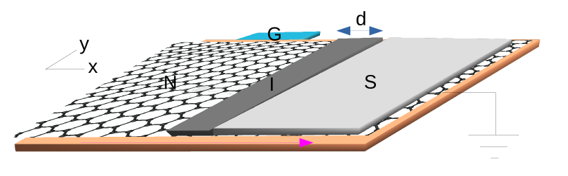
In this work we consider a normal-insulator-superconductor (NIS) set-up of silicene in plane as depicted in Fig. 1 with normal region (N) being in . The insulating region (I) with width has while the superconducting region (S) occupies 0 for all . The insulating region has a barrier potential which can be implemented by an external gate voltage. Also the chemical potential can be tuned by a gate voltage connected to the silicene sheet (see. Fig. 1). Superconductivity in silicene is induced via the proximity effect of a bulk -wave superconductor placed close to the silicene sheet in the region .
Silicene NIS junction can be described by the Dirac Bogoliubov-de Gennes (DBdG) equation of the form Linder and Yokoyama (2014)
| (3) |
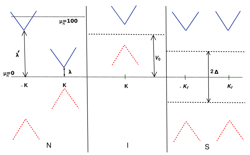
where is the excitation energy, is the proximity induced superconducting pairing gap and is given by Eq.(2). The schematic band diagram of the silicene NIS set-up is shown in Fig. 2. In silicene, the pairing occurs between , and , as well as , and , for a -wave superconductor.
Solving Eq.(3) we find the wave functions in three different regions. The wave functions for the electrons and holes moving in direction in normal silicene region reads
| (4) |
where the normalization factors are given by , and
| (5) |
| (6) |
| (7) |
Here is the chemical potential in the normal silicene region.
Due to translational invariance in the -direction, corresponding momentum is conserved. The angle of incidence and the Andreev reflection (AR) angle are related via the relation
| (8) |
For the rest of the paper, we have denoted the band gap at valley by and the gap at valley by . In the Insulating region wave functions can be found from normal region wave functions (Eq.(4)) by replacing .
In the Superconducting region the wave functions of DBdG quasiparticles are given by,
| (9) |
Here, and . The transmission angles for electron-like and hole-like quasi-particles are given by,
| (10) |
for The quasiparticle momentums can be written as
| (11) |
where and is the gate potential applied in the superconducting region to tune the Fermi surface mismatch. The requirement for the mean-field treatment of superconductivity is that Beenakker (2006, 2008).
We consider electrons with energy incident at the interface of our NIS junction of a silicene sheet. Considering both normal reflection and Andreev reflection from the interface, we can write the wave functions in three different regions of the junction as
| (12) |
where and are the amplitudes of normal reflection and Andreev reflection in the N region respectively. and denote the amplitudes of transmitted electron like and hole like quasiparticles in the S region. Using boundary conditions at the two interfaces, we can write
| (13) |
From these equations we can find the reflection and AR amplitudes and , required for evaluating the electronic contribution of TC. For the NIS junction, normalized thermal conductance is given by Bardas and Averin (1995); Yokoyama et al. (2008)
| (14) | |||||
Here, and are reflection and AR probability respectively. From current conservation, we obtain Linder and Yokoyama (2014)
| (15) |
III Thin barrier
In this section, we present our numerical results based on Eq.(14) for the thin barrier limit. In this particular limit of insulating barrier, we consider and , such that where are the electron and hole momentum inside the insulating barrier respectively. is defined as the barrier strength of the insulating region. Such limit has been considered before in Ref. Bhattacharjee and Sengupta, 2006 for the analysis of tunneling conductance in graphene.
We take to be very large compared to the superconducting pairing potential . For simplicity, we consider and in Eq.(10) and Eq.(11). Due to significant chemical potential imbalance between the normal and superconducting sides, there is a large mismatch of Fermi wavelengths in these two sides resulting in interesting behavior in TC.
Before proceeding to present our numerical results, here we illustrate whether both valleys contribute to TC at all doping conentrations or not. For silicene, the band gap at valley satisfies for the undoped and moderately doped regime. Consequently, valley does not contribute to TC in these two regimes. Nevertheless, in highly doped regime, which is much larger than both the band gaps and at and valley respectively (see Fig. 2). Hence, we consider contribution for both the valleys while calculating TC for the highly doped regime. Therefore, we can write in this case. On the other hand, for the undoped and moderately doped case.

III.1 Undoped regime ()
In this subsection we present our results when the normal region of the silicene sheet is undoped i.e. . In Fig. 3((a)-(d)) we show the behavior of TC as a function of for ranging from to . In silicene can be tuned by just the external electric field . We choose various barrier strengths. Here, is the transition temperature of the superconducting silicene. The exponential fall of TC () when the temperature is below the transition temperature results because of spherical symmetry of the -wave superconductor Yokoyama et al. (2008). This behavior is similar to that of conventional nomal metal-superconductor junction Bezuglyi and Vinokur (2003). As we increase by suitably adjusting the perpendicular electric field , TC decreases monotonically. As i.e. band gap increases, the available propagating states through which thermal transport takes place reduces and as a consequence TC decreases monotonically with . However, as carriers with all energies contribute to the thermal transport, quantitative value of is hardly affected by change of band gap at Dirac points which is less than the induced superconducting gap in magnitude. This we can see from formula of (see Eq.(14)).
In Fig. 4((a)-(d)) we demonstrate the bahavior of TC with respect to the barrier strength . We choose different temperatures below the transition temperature . TC exhibits a periodic behavior with periodicity as shown in Fig. 4. Such periodic behavior of TC is entirely different from conventional NS junction where TC always decays with the barrier strength. This periodic behavior is also the manifestation of Dirac fermions in silicene. When temperature is very small compared to , the quantitative value of is vanishingly small which can also be seen from Fig. 3 focusing at small region. Also, the periodicity of TC is independent of value. Moreover, for the regime, the major contribution in TC originates from the specular Andreev reflection (SAR) Beenakker (2006) process due to the pecularity of 2D Dirac systems. Effect of is more prominent near the transition temperature because superconducting gap decreases as resulting the band gap in the normal region to overcome the superconducting pairing gap. As a result normal reflection probability enhances rusulting in reduction in . Note that, the maxima of the peaks of for different are same for which is unique behavior at very low temperature (). On the contrary, peak heights of gets reduced due to the evanescent modes as long as approaches .
The oscillatory behavior of the TC can be explained as follows. Nonrelativistic free electrons with energy incident on a potential barrier with height are described by an exponentially decaying (non-oscillatory) wave function inside the barrier region if , since the dispersion relation is . On the contrary, relativistic free electrons satisfies a dispersion , consequesntly corresponding wave functions do not decay inside the barrier region Linder and Sudbø (2007). Instead, the transmittance of the junction displays an oscillatory behavior as a function of the strength of the barrier. Hence, the undamped oscillatory behavior of TC at is a direct manifestation of the relativistic low-energy Dirac fermions in silicene.


III.2 Moderately doped regime ()
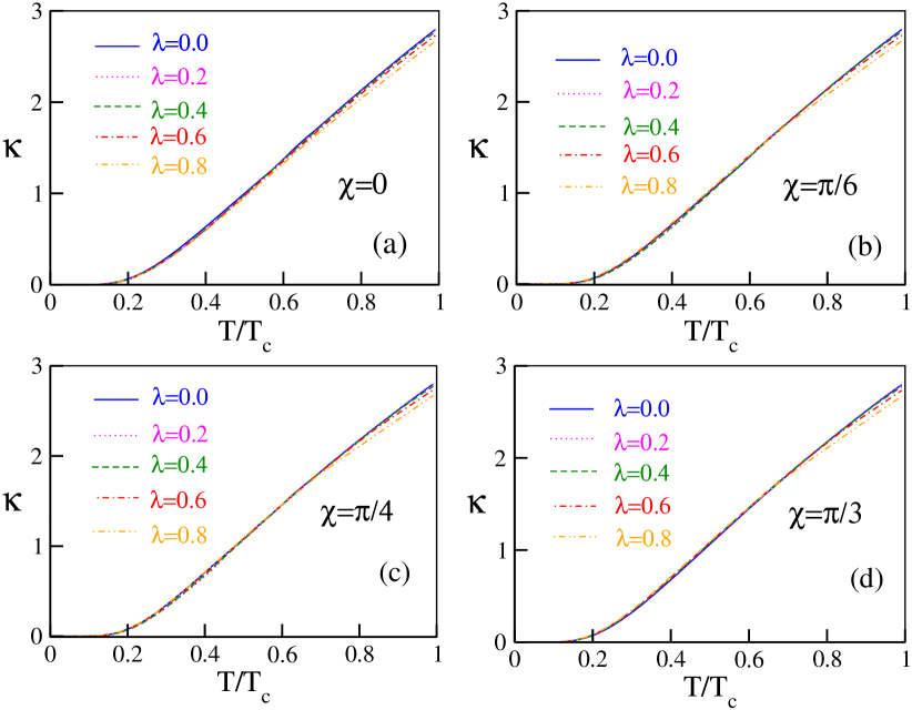
In this subsection, we present our results for the moderate doping case where chemical potential in the normal part of the silicene sheet is . This regime is qualitatively different from the undoped one because the doping concentration has now almost same order of magnitude with . So it is interesting to analyse whether non-trivial behavior of TC emerges out due to the interplay between doping and band gap at the two valleys. In Fig. 5((a)-(d)), TC is shown as a function of temperature with different and for various barrier strength . The striking difference from the undoped case is that does not show monotonic behavior with . When , decreases with increasing value by from 0 to 0.4. Then further increases as crosses value. At temperaure close to , decreases monotonically with increasing similar to the undoped case. Note that, decreases in the regime due to the evanescent modes present between the energy range to . Then start increasing in the subgapped regime when resulting in the non-monotonic behavior. As long as it again decreases due to the silicene band gap like the case.
Transition from non-monotonic to monotonic behavior of TC takes place at independent of value. This non-monotonic characteristics is more promiment in Fig. 6((a)-(b)) where oscillatory nature of with barrier strength is presented for different values of . For a fixed , such non-monotonic characteristics of can be tuned by the external electric field which is unique in silicene. Here also the periodicity of oscillations remains independent of temperature and contribution in originates from both SAR and retro AR.
III.3 Highly doped regime ()
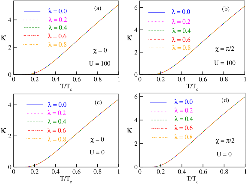
Here in this subsection we present the features of TC while normal portion of silicene is highly doped (). In this case the mean-field condition: Beenakker (2006) can be satisfied by assuming or taking as before. Former one does not exhibit any Fermi surface mismatch between the normal and superconducting regions. On the other hand, the latter one contributes to large density mismatch between the two sides. We have numerically calculated for , and regime. The corresponding results are presented in Fig. 7 and Fig. 8. Here also, similar to the undoped and moderately doped regime, has exponential dependance on temperature which is a universal feature in thermal transport. The only difference from the previous two cases lies in the fact that we consider the separate contribution of both the valleys and when (see Fig. 2).
From analytical expressions of the superconducting wave functions (see Eq.(10) and Eq.(11)), we notice that the change in wave functions due to the variation of and is negligible because . Hence, in this regime comes out to be independent of the applied electric field which is depicted in Fig. 7. The corresponding behavior is independent of also. Nevertheless, the quantitative value of is enhanced by a factor of “” compared to the previous two cases due to the contribution coming from both the valleys.
The oscillatory behavior of TC with respect to the barrier strength persists in the highly doped regime as well (see Fig. 8((a)-(d))). However, now the periodicity changes with the value. As long as , period remains but it increases gradually to as decreases towards . Both for and , periodicity of remains same at but the spread of the curve decreases as decreases as depicted in Fig. 8(a,c). This change of behavior with variation of can be qualitatively understood from Fermi surface mismatch between the normal and superconducting sides. For large Fermi wavelengths mismatch between the normal and superconducting regions, period of oscillations remains which is similar to the undoped and moderately doped regimes. However, as the Fermi wavelengths mismatch becomes vanishingly small in the highly doped regime, periodicity of oscillation converts to . Here also, as well as have neglizible effect on the thermal transport as is the dominant energy scale in this particular regime. Similar periodicity of in the behavior of tunneling conductance in graphene for the highly doped regime was reported earlier in Ref. Bhattacharjee and Sengupta, 2006.
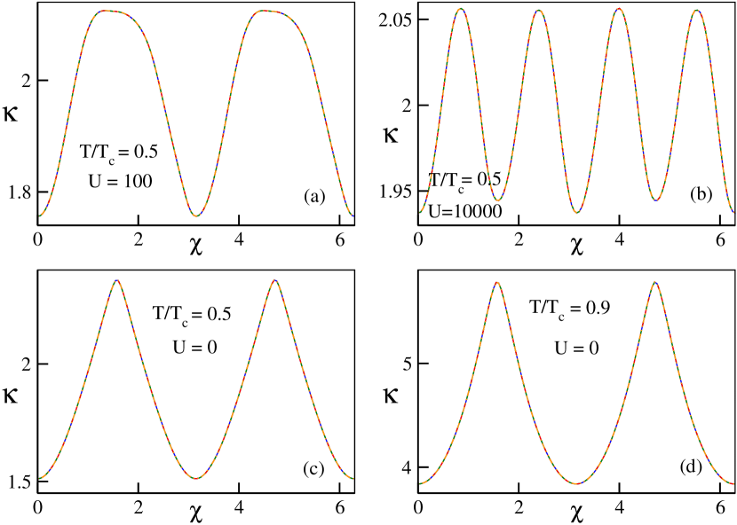
Note that, for the highly doped regime, major contribution in originates from the retro AR in contrast to SAR in the undoped regime. Also the periodicity of changes from to as long as . Such change of periodicity with doping, in the behavior of thermal conductance in the thin barrier limit, can be an indirect way to identify the crossover from SAR to retro AR in Dirac materials. Although, it is not apparent to compute separately the individual contribution of retro AR and SAR to when . This is because within our scattering matrix formalism we have to average over all values of energy (see Eq.(14)). Hence, the change of periodicity of from to may not be a strong justification (smoking gun signal) for the crossover phenomenon from SAR to retro AR as the periodicity again can change from to due to Fermi wavelengths mismatch between the normal and superconducting regions even if where the major contribution to arising from retro AR (see Fig. 8(b)). However, to observe the latter change, one has to enhance the doping concentration in the superconducting side also.
IV Thick barrier
In this section we examine TC in the thick barrier limit where we consider a barrier of width and height . The height of the barrier can be tuned by applying an additional gate voltage in the insulating region Bhattacharjee et al. (2007). We emphasize on the role being played by the barrier height as well as thickness . We show manifests osscillatory behavior with respect to both and . However, the period of oscillation is no longer universal as in the thin barrier limit but beocmes a function of applied voltage and width . Similar feature is found earlier in graphene NIS junction Bhattacharjee et al. (2007) where tunneling conductance is shown to have oscillation whose period depends on .
Note that, in the thick barrier limit, extended BTK formalism Blonder et al. (1982) is valid for our model of NIS junction if where which is the phase coherence length in the superconducting side. Fermi wavelength is given by, where being the Fermi wave vector. So and are related by, . We notice that undoped regime is not valid in the thick barrier limit becuase Fermi wavelength diverges in that regime. In the moderately doped regime, choosing as before, we obtain .
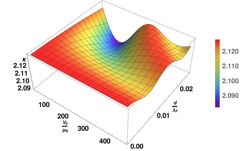
IV.1 Moderately doped regime ()
When the doping concentration is moderate () in the normal silicene regime, TC exhibits similar features as in the thin barrier limit. Here we illustrate the behavior of TC as a function of barrier height and thickness in Fig. 9 and Fig. 10 for and respectively. We note the following features. (i) When , TC is unaffected by the barrier height . This is true for arbitray bandgap as we can see from Fig. 9 and Fig. 10. Nonetheless, affects TC as increases. Qualitatively we understand that as is chosen to be large , small barrier height has negligible effect on TC. (ii) As barrier height dominates , TC exhibits oscillatory behavior as a function of and such oscillation persists even for very large values of . Similarly oscillation is present as changes even for . However, the period of oscillation does not show any universal periodicity of like in the thin barrier case. The period of oscillation of depends on both and . Similar feature was found earlier in case of tunneling conductance in graphene NIS junction Bhattacharjee et al. (2007). (iii) The external electric field does not change the qualitative behavior of as shown in Fig. 9 and Fig. 10. Although it changes the quantitative value of . As increases by tuning , TC reduces monotonically with both and similar to the thin barrier case when .

IV.2 Highly doped regime ()
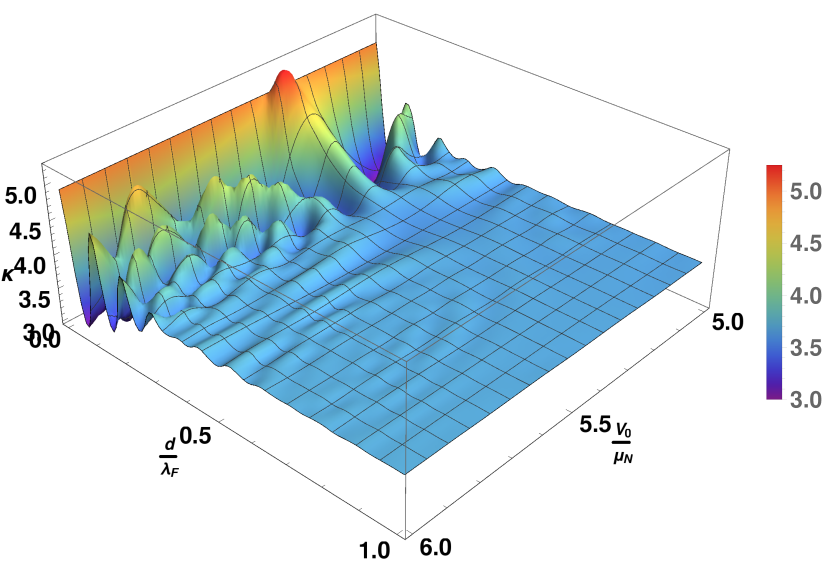
Here, we present the behavior of TC as a function of and with high doping concentration where . We choose only. Hence, there is no Fermi wavelength mismatch between the normal and superconducting side of the silicene sheet. Thus the effect of applied gate voltage across the insulating region can be investigated prominently in this regime due to . Also, as we have already pointed out in thin barrier limit that and has negligible effect on when , hence we consider and .
Fig. 11 represents TC as a function of and for and . We choose value to be much larger than in order to investigate the effect of applied gate voltage or barrier height on TC. We note that exhibits oscillation with respect to even for very small barrier thickness . The period of these oscillations is entirely dependent on . As mentioned earlier, such oscillations of at very small does not appear at moderate doping concentration unless and until exceeds . Note that, the enhancement in the quantitative value of compared to the previous case arises due to both and valley contribution. Also in the highly doped regime, the amplitudes of oscillations of decay after a certain value of barrier thickness () for arbitrary barrier height . This can be understood from the Fermi wave-length mismatch between the barrier and the normal silicene region for high value of and . This feature of TC is in sharp contrast to the tunneling conductance in graphene which is oscillatory for arbitrary and Bhattacharjee et al. (2007).
V Summary and conclusions
To summerize, in this article, we investigate thermal conductance by Dirac fermions in silicene NIS junction where superconductivity is induced in silciene sheet through the proximity effect. We study the behavior of TC in this set-up both for thin and thick insulating barrier limit. We show that TC exhibits periodic oscillation with respect to the barrier strength in thin barrier limit for undoped () and moderately doped () regime where the Fermi surface mismatch between the normal and superconducting sides is significant. The oscillation becomes periodic as a function of barrier strength in the highly doped () regime where Fermi surfaces in the two sides are almost aligned. This change of periodicity ( to ) in thermal response with the variation of doping concentration can be an indirect probe to identify the crossover from SAR to retro AR. Nonetheless, TC shows conventional exponential dependence on temperature independent of doping concentration and barrier characteristics. The external electric field reduces TC monotonically in the undoped regime. However, a non-trivial interplay between band gap at Dirac points and doping concentration appears in the moderately doped case. Consequently, electric field can tune TC in the later regime. On the other hand, electric field has negligible effect on TC when .
In the thick barrier limit, oscillation of TC persists both as a fucntion of barrier thickness as well as barrier height . The latter can be tuned by an additional gate voltage appled at the insulating region. However, we show that the periodicity of TC no longer remains constant, rather becomes functions of both and . Also after a certain barrier thickness (), amplitude of oscillations in TC decays for arbitrary in the highly doped regime.
In our analysis, we consider only the electronic contribution in TC and neglect the phonon contribution at small temperatures (). Very recently, nanoscale control of phonon excitation in graphene has been reported Kim et al (2015). Hence, such nanoscale control of phonon excitation in silicene and the effect of electron-phonon interaction on TC will be presented elsewhere.
As far as experimental realization of our silicene NIS set up is concerned, superconductivity in silicene can be induced by -wave superconductor like Heersche et al. (2007); Choi et al. (2013). In recent years, proximity induced superconductivity has been observed in other 2D materials such as graphene Heersche et al. (2007); Choi et al. (2013); Calado et al. (2015) and transition metal dichalcogenides Shi et al. (2015). Once such superconducting proximity effect is realized in silicene, fabrication of silicene NIS junction can be feasible. Typical spin-orbit energy in silicene is while the buckling parameter Liu et al. (2011a); Ezawa (2015a). Considering Ref. Heersche et al., 2007, typical induced superconducting gap in silicene would be . For such induced gap, choosing , we obtain . Hence, a barrier of thickness may be considered as thin barrier and the gate voltage can therefore meet the demands of our silicene NIS setup. For the thick barrier limit, thickness can be varied arbitrarily (satisfying ), with the gate voltage .
However, the effects of external electric field might not be visible in the above regime as envisaged by our theoretical calculation. To realize non-trivial effects due to the electric field on TC, chemical potential in the normal silicene region can be and the external electric field can be within the range . In this moderately doped regime (), the criterion for and can be similar to the highly doped regime as mentioned before.
Note that, in our analysis, we have considered a bulk silicene material following Ref. Linder and Yokoyama, 2014. The bulk-boundary correspondence has not been taken into account within our scattering matrix formalism. So, we cannot distinguish between the topological phase or the band insulating phase within our formalism even if we tune the electric field in our calculation. Hence, in our analysis, the contribution in the thermal conductance is arising from the bulk states only.
We expect our results to be analogous to the recently discovered 2D materials like germenene, stanene Dávila et al. (2014); Zhu et al. (2015). Although the effect of Rashba SOC in these materials can be more important than silicene Liu et al. (2011a); Ezawa (2015a). For silicene, is small compared to Ezawa (2012a). The low energy spectrum of silicene is independent of only at the Dirac point Ezawa (2012a). Inclusion of small breaks the spin symmetry and spin is no longer a good quantum number. Qualitatively, from scattering point of view, presence of small introduces spin flip scattering processes from the normal-superconductor (NS) interface. Apart from spin conserving reflection and AR processes, the reflection and AR processes with spin flip also contribute to . Nevertheless, as is small, the amplitudes of those additional scattering processes will also be small. Hence, after averaging over all the energy values while computing , the contribution arising from these two extra scattering processes on the resulting thermal conductance will be vanishingly small. Thus the qualitative feature of as a function of or will remain similar even one includes small into account.
Acknowledgements.
We acknowledge S. D. Mahanti for valuable discussions and encouragement at the initial stage of this work.References
- Geim and Novoselov (2007) A. K. Geim and K. S. Novoselov, Nat. Materials 6, 183 (2007).
- Castro Neto et al. (2009) A. H. Castro Neto, F. Guinea, N. M. R. Peres, K. S. Novoselov, and A. K. Geim, Rev. Mod. Phys. 81, 109 (2009).
- Qi and Zhang (2011) X. L. Qi and S. C. Zhang, Rev. Mod. Phys. 83, 1057 (2011).
- Hasan and Kane (2010) M. Z. Hasan and C. L. Kane, Rev. Mod. Phys. 82, 3045 (2010).
- Liu et al. (2011a) C.-C. Liu, H. Jiang, and Y. Yao, Phys. Rev. B 84, 195430 (2011a).
- Houssa et al. (2015) M. Houssa, A. Dimoulas, and A. Molle, J. Phys. Cond. Matt. 27, 253002 (2015).
- Ezawa (2015a) M. Ezawa, J. Phys. Soc. Jpn. 84, 121003 (2015a).
- (8) A. Hattori, S. Tanaya, K. Yada, M. Araidai, M. Sato, Y. Hatsugai, K. Shiraishi, and Y. Tanaka, arXiv:1604.04717 [cond-mat.mes-hall] .
- Lalmi et al. (2010) B. Lalmi, H. Oughaddou, H. Enriquez, A. Kara, S. Vizzini, B. Ealet, and B. Aufray, Appl. Phys. Lett. 97, 223109 (2010).
- Padova et al (2010) P. D. Padova et al, Appl. Phys. Lett. 96, 261905 (2010).
- Vogt et al. (2012) P. Vogt, P. D. Padova, C. Quaresima, J. Avila, E. Frantzeskakis, M. C. Asensio, A. Resta, B. Ealet, and G. L. Lay, Phys. Rev. Lett. 108, 155501 (2012).
- Lin et al. (2012) C.-L. Lin, R. Arafune, K. Kawahara, N. Tsukahara, E. Minamitani, Y. Kim, N. Takagi, and M. Kawai, Appl. Phys. Exp. 5, 045802 (2012).
- Zutić et al. (2004) I. Zutić, J. Fabian, and S. Das Sarma, Rev. Mod. Phys. 76, 323 (2004).
- Tsai et al. (2013) W.-F. Tsai, C.-Y. Huang, T.-R. Chang, H. Lin, H.-T. Jeng, and A. Bansil, Nat. Commn. 4, 1500 (2013).
- Wang et al. (2012) Y. Wang, J. Zheng, Z. Ni, R. Fei, Q. Liu, R. Quhe, C. Xu, J. Zhou, Z. Gao, and J. Lu, Nano 7, 1250037 (2012).
- Wang et al. (2015) Y. Wang, R. Quhe, D. Yu, J. Li, and J. Lu, Chin. Phys. B 24, 087201 (2015).
- Rachel and Ezawa (2014) S. Rachel and M. Ezawa, Phys. Rev. B 89, 195303 (2014).
- Ezawa (2013) M. Ezawa, Phys. Rev. B 87, 155415 (2013).
- Pan et al. (2014) H. Pan, Z. Li, C.-C. Liu, G. Zhu, Z. Qiao, and Y. Yao, Phys. Rev. Lett. 112, 106802 (2014).
- Kundu et al. (2016) A. Kundu, H. Fertig, and B. Seradjeh, Phys. Rev. Lett. 116, 016802 (2016).
- Yokoyama (2013) T. Yokoyama, Phys. Rev. B. 87, 241409(R) (2013).
- Saxena et al. (2015) R. Saxena, A. Saha, and S. Rao, Phys. Rev. B 92, 245412 (2015).
- Tao et al. (2015) L. Tao, E. Cinquanta, D. Chiappe, C. Grazianetti, M. Fanciulli, M. Dubey, A. Molle, and D. Akinwande, Nat. Nanotechnol. 10, 227 (2015).
- Ezawa (2012a) M. Ezawa, New J. Phys. 14, 033003 (2012a).
- Houssa et al. (2013) M. Houssa, B. van den Broek, E. Scalise, G. Pourtois, V. Afanas’ Ev, and A. Stesmans, Phys. Chem. Chem. Phys. 15, 3702 (2013).
- Drummond et al. (2012) N. Drummond, V. Zolyomi, and V. Fal’Ko, Phys. Rev. B 85, 075423 (2012).
- Liu et al. (2011b) C. C. Liu, W. Feng, and Y. Yao, Phys. Rev. Lett. 107, 076802 (2011b).
- Ezawa and Nagaosa (2013) M. Ezawa and N. Nagaosa, Phys. Rev. B. 88, 121401(R) (2013).
- Ezawa (2012b) M. Ezawa, Eur. Phys. J. B 85, 363 (2012b).
- Ezawa (2015b) M. Ezawa, Phys. Rev. Lett. 114, 056403 (2015b).
- Beenakker (2008) C. W. J. Beenakker, Rev. Mod. Phys. 80, 1337 (2008).
- Linder and Yokoyama (2014) J. Linder and T. Yokoyama, Phys. Rev. B. 89, 020504(R) (2014).
- Xu et al. (2014) Y. Xu, G. Zhongxue, and S. C. Zhang, Phys. Rev. Lett. 112, 226801 (2014).
- Lundgren et al. (2014) R. Lundgren, P. Laurell, and G. A. Fiete, Phys. Rev. B. 90, 165115 (2014).
- Chandrasekhar (2009) V. Chandrasekhar, Supercond. Sci. Technol. 22, 083001 (2009).
- Machon et al. (2014) P. Machon, M. Eschrig, and W. Belzig, New J. Phys. 16, 073002 (2014).
- Ozaeta et al. (2014) A. Ozaeta, P. Virtanen, F. S. Bergeret, and T. T. Heikkilä, Phys. Rev. Lett. 112, 057001 (2014).
- Yokoyama et al. (2008) T. Yokoyama, J. Linder, and A. Sudbø, Phys. Rev. B 77, 132503 (2008).
- Wysokiński (2014) M. Wysokiński, Acta Physica Polonica, A. 126 (2014).
- Salehi et al. (2010a) M. Salehi, M. Alidoust, Y. Rahnavard, and G. Rashedi, J. Appl. Phys. 107, 123916 (2010a).
- Salehi et al. (2010b) M. Salehi, M. Alidoust, and G. Rashedi, J. Appl. Phys. 108, 083917 (2010b).
- Andreev (1964) A. Andreev, Sov. Phys. JETP 46 (1964).
- Bezuglyi and Vinokur (2003) E. Bezuglyi and V. Vinokur, Phys. Rev. Lett. 91, 137002 (2003).
- Bhattacharjee et al. (2007) S. Bhattacharjee, M. Maiti, and K. Sengupta, Phys. Rev. B 76, 184514 (2007).
- Beenakker (2006) C. W. J. Beenakker, Phys. Rev. Lett. 97, 067007 (2006).
- Bardas and Averin (1995) A. Bardas and D. Averin, Phys. Rev. B. 52, 12873 (1995).
- Bhattacharjee and Sengupta (2006) S. Bhattacharjee and K. Sengupta, Phys. Rev. Lett. 97, 217001 (2006).
- Linder and Sudbø (2007) J. Linder and A. Sudbø, Phys. Rev. Lett. 99, 147001 (2007).
- Blonder et al. (1982) G. Blonder, M. Tinkham, and T. Klapwijk, Phys. Rev. B. 25, 4515 (1982).
- Kim et al (2015) H. W. Kim et al, Nat. Commn. 6, 7528 (2015).
- Heersche et al. (2007) H. B. Heersche, P. Jarillo-Herrero, J. B. Oostinga, L. M. K. Vandersypen, and A. F. Morpurgo, Nature 446, 56 (2007).
- Choi et al. (2013) J.-H. Choi, G.-H. Lee, S. Park, D. Jeong, J.-O. Lee, H.-S. Sim, Y.-J. Doh, and H.-J. Lee, Nat. Commn. 4, 2525 (2013).
- Calado et al. (2015) V. E. Calado, S. Goswami, G. Nanda, M. Diez, A. R. Akhmerov, K. Watanabe, T. Taniguchi, T. M. Klapwijk, and L. M. K. Vandersypen, Nat. Nanotechnol. 10, 761 (2015).
- Shi et al. (2015) W. Shi, J. Ye, Y. Zhang, R. Suzuki, M. Yoshida, J. Miyazaki, N. Inoue, Y. Saito, and Y. Iwasa, Sci. Rep. 5, 12534 (2015).
- Dávila et al. (2014) M. Dávila, L. Xian, S. Cahangirov, A. Rubio, and G. Le Lay, New J. Phys. 16, 095002 (2014).
- Zhu et al. (2015) F.-f. Zhu, W.-j. Chen, Y. Xu, C.-l. Gao, D.-d. Guan, C.-h. Liu, D. Qian, S.-C. Zhang, and J.-f. Jia, Nat. Mat. 14, 1020 (2015).