Electronic, Optical and Mechanical Properties of Silicene Derivatives
Abstract
Successful isolation of graphene from graphite opened a new era for material science and condensed matter physics. Due to this remarkable achievement, there has been an immense interest to synthesize new two dimensional materials and to investigate their novel physical properties. Silicene, form of Si atoms arranged in a buckled honeycomb geometry, has been successfully synthesized and emerged as a promising material for nanoscale device applications. However, the major obstacle for using silicene in electronic applications is the lack of a band gap similar to the case of graphene. Therefore, tuning the electronic properties of silicene by using chemical functionalization methods such as hydrogenation, halogenation or oxidation has been a focus of interest in silicene research. In this paper, we review the recent studies on the structural, electronic, optical and mechanical properties of silicene-derivative structures. Since these derivatives have various band gap energies, they are promising candidates for the next generation of electronic and optoelectronic device applications.
pacs:
62.25.-g, 73.20.At, 68.47.Gh, 78.67-nI Introduction
Layered bulk materials consisting of two dimensional (2D) sheets which are hold together with weak, interlayer van der Waals interaction have been the focus of interest for more than a centuryBrodie ; Peierls1 ; Peierls2 . With the advancement of synthesis and characterization techniques it has been possible to isolate ultra thin films down to a monolayer of these materials which became feasible in the last decade. Monolayer forms of these layered bulk materials often exhibit different physical properties than their bulk counterparts. The first isolated 2D material is known to be graphene, a one-atom-thick carbon sheet, with extraordinary physical propertiesNovo1 ; Novo2 ; Geim1 . After the successful exfoliation of graphene by Novoselov and Geim, researchers have been searching for several other 2D materials that can exist in single layer form such as hexagonal monolayer crystals III-V binary compoundshasan1 ; Golberg ; Zeng ; Song ; Bacaksiz ; Zhuang ; QWang ; KKim ; MFarahani , transition metal dichalcogenides (TMDs)Wang ; Wilson ; Horzum ; Bacaksiz2 and the group IV elements (silicene, germanene, stanene)Cahangirov ; Vogt ; Lin ; Fleurence ; Davila ; Zhu . Among these 2D monolayer materials, graphene and silicene are known to posses semi-metallic character while the members of TMDs family compounds generally display semiconducting behavior with a band gap of 1-2 eV. In all of these 2D materials silicene occupies an important position for the next generation of nanoscale technology which up to now is mostly based on silicon.
According to its electronic-band structure, graphene has a semi-metallic character which is not suitable for optoelectronic applications. One possible way to open a gap in the band structure of graphene is to functionalize its surface with various types of atoms such as H, F and Cl which were widely studied and successfully synthesized. It was shown that both full and partial hydrogenation of graphene leads to semiconducting materials with different band gap valuesBoukhvalov ; Haberer ; Sofo . Similar to the hydrogenation case, experimental and theoretical studies showed that the band gap of fluorinated-graphene can alter from 0 to 3 eV depending on the fluorination level. cRobinson ; cSamarakoon ; cCheng1 ; cJeon ; cGarcia
Silicene, a 2D honeycomb structure of Si atoms with a buckled geometry, has been attracting great interest due to its physical properties such as possessing massless Dirac fermions and large spin-orbit coupling resulting in an intrinsic band gapKara ; Xu1 . The buckled structure of silicene is a consequence of sp2-sp3 hybridization of Si atoms. This makes the structure of silicene different from the flat structure of graphene. Another important physical property of silicene is its high surface reactivity which widens the methods of manipulating its electronic, magnetic and mechanical propertieshasan2 . Thus, the functionalization of its surface and applying external mechanical strain are some of the widely used ways of controlling the electronic properties of silicene for its practical usage in device technology.
After the theoretical prediction and successful synthesis of silicene, researchers have focused on dopingLin2 ; Quhe ; Ni ; Cheng ; Sivek ; Zheng , chemical modificationhasan2 ; Okamoto1 ; Nakano ; Okamoto2 ; Sugiyama ; Pereda ; Spencer ; Du and strain engineeringLiu12 ; Qin12 ; Zhao12 ; Hu13 ; Kal-13 ; Dur14 ; Moh14 ; Hus14 ; Wang14 ; Zhu14 ; Yang14 ; Cao15 in order to modify its electronic structure. Studies have demonstrated that fully hydrogenated silicene is a semiconductorDing ; Voon ; Houssa while half hydrogenated silicene is still a semi-metal or direct-gap semiconductor depending on the hydrogenation configurationZhang . Functionalization of silicene with halogen atoms (F, Cl, Br and I) was also considered in several studies for tuning its electronic structureWei ; Gao ; Zhang2 ; Wang2 . Studies on fully halogenated silicene indicated that it possesses a direct-gap semiconducting character with various band gap depending on the type of the halogen atom. Other functionalization methods like doping organic molecules on hydrogenated silicene have also been considered. Okamoto1 ; Nakano ; Okamoto2 ; Sugiyama Moreover, the oxidation of silicene was studied both theoretically and experimentally by several research groups which is important for the use of 2D materials in nanoscale device technology. Padova1 ; Padova2 ; Molle ; Friedlein ; Xu ; Liu
In this review we summarize the studies on the structural, electronic, optical and mechanical properties of silicene derivatives. This review is organized as follows: We first provide the physical properties of hydrogenated silicene in Sec. II, the oxidized silicene in Sec. III and the halogenated silicene in Sec IV. The physical properties of silicene functionalized with organic molecules are given in Sec. V while the properties of silicene decorated with adatoms are given in Sec. VI. Finally we present a brief summary in Sec. LABEL:summ
II HYDROGENATED SILICENE
In this section we review the results of studies on hydrogenation of silicene. Like C atoms in graphene, Si atoms in silicene have unpaired electrons which are suitable for possible functionalizations. Among these possible functionalizations, hydrogenation was studied extensively in the literature. Zhang ; Drissi1 ; Drissi2 ; Zhang3 It has been shown that two possible configurations exist for the hydrogenation process of silicene, fully-hydrogenation (fH), namely silicane, and single side hydrogenation, half-hydrogenation (hH), similar to the case of graphene.
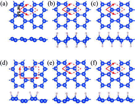
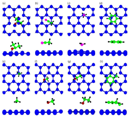
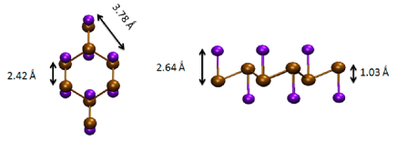
In Fig. 1, possible geometric structures are given for bare, fully and half hydrogenated silicene crystals. Zhang et al. investigated the structural properties of fH and hH cases of silicene by first principles calculationsZhang and found that for the silicane structure the chair-like configuration (see Fig. 1(c)) is the ground state and it has 30 meV/atom lower energy than the boat-like one (see Fig. 1(b)) as confirmed by total energy calculations. The Si-H bond length was calculated to be 1.50 Å for the chair-like structure. For the hH silicene they reported that the zigzag structure (Fig. 1(d)) is the most stable configuration with a total energy of 33 meV/atom and 180 meV/atom lower than the boat-like and chair-like structures, respectively. In addition, Osborn et al. reported that the fH silicene structure has a higher buckling than its bare formOsborn . They calculated the buckling height of fH silicene to be 0.74 Å while 0.54 Å was reported for the bare silicene case. This structural change occurs due to the interaction between Si and H atoms which widens the structure in the vertical direction. The buckling height of the hH silicene structure is reported to be less than that of silicane as expectedZhang4 .
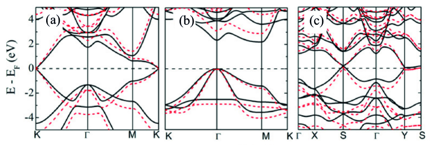
Hydrogenation plays an important role for tuning the electronic structure of a 2D material. For instance in contrast to bare graphene, hydrogenated graphene, namely graphane, is a semiconductorSahin3 . The same functionalization process was studied in the case of silicene. Zhang et al. reported that the electronic-band structure of silicene can be tuned through hydrogenation. It was found that silicane is an indirect-gap semiconductor with its valence-band maximum (VBM) and conduction band minimum (CBM) residing at the and M points, respectively. The band gap of silicene was found to be 2.36 eV within GGA approximation while it is reported as 3.51 eV by using HSE06 functional. These results were also predicted and supported by many other studiesDing ; Houssa ; Zhang ; Osborn . In contrast to silicane, the HH silicene crystal possesses metallic character in its zigzag structure (see Fig. 2(c)). However, the other two configurations, boat-like and chair-like structures, were reported to be direct-gap semiconductorsZhang .
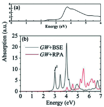
Optical properties of silicane such as its optical absorption spectrum and dielectric function were investigated in the literature beforeWei ; Chinnathambi . In addition, the optical properties of bilayer and few layer fH silicene structures were also predictedHuang ; Liu2 . Chinnathambi et al. studied the optical properties of silicane by calculating the optical absorption spectrumChinnathambi . They reported that a transition from semi-metallic to semiconducting behavior is seen. The reason is the broken bonds in silicene due to the saturation by H atoms. As seen in Fig. 3(a), an absorption onset at 2.2 eV was predicted which is consistent with the bandgap of silicane as calculated within the GGA approximationChinnathambi . Moreover, Wei et al. investigated the optical absorption spectra of silicane by GW approximation with random phase approximation (GW+RPA) and Bethe-Salpeter equation (GW+BSE)Wei . It was reported that the hydrogenation process removes conduction at the Dirac point and causes a finite band gap opening. It was also reported that the GW+RPA and GW+BSE methods give different absorption spectra due to the large self-energy correlations of electrons (see Fig. 3(b)). The absorption onset obtained with GW+RPA is located at about 4 eV consistent with the band gap value calculated within HSE06 functionalHoussa ; Zhang . Including the excitonic correlations of electrons and holes, within the GW+BSE approximation, the excitonic effect significantly shifts the onset of the absorption spectrum towards lower energy (see Fig. 3(b)).
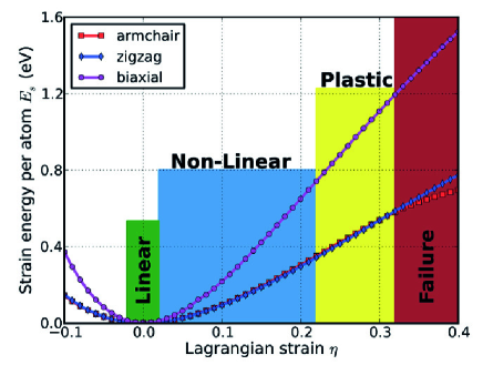
In addition to the electronic and optical properties, the mechanical properties of silicane were also investigated theoretically in the previous studiesJamdagni ; Peng ; Yang . Peng et al. reported that the in-plane stiffness (58 N/m) and Poisson ratio (0.24) values for silicane are reduced by 16% and 26%, respectively, when compared to those of silicenePeng . The elastic limits in terms of ultimate tensile strains were found to be 0.22, 0.28, and 0.25 along armchair, zigzag, and biaxial directions, respectively. It was reported that these values increases by 9%, 33%, and 24%, respectively from silicene to silicane. Moreover, Jamdagni et al. reported that the band gap of silicane reduces to zero with increasing applied biaxial tensile strain leads to a semiconducting to metallic transition for silicane. Their calculations indicated that at 2% of tensile strain, the magnitude of the bandgap first increases to 2.22 eV and the indirect band-gap character of silicane changes to a direct bandgap. Then with every 2% increment of tensile strain, the band gap decreases nearly by 0.3 eV and the 22% value of the strain is the critical value for semiconducting-to-metallic transitionJamdagni .
III OXIDATION OF SILICENE
Oxidation has important consequences on the usage of materials in real life device technologies. Thus, the oxidation processes of both bulk and 2D materials were widely studied and investigated in previous works. Similar to all materials, the oxidation of silicene is an important question for scientists during the fabrication of silicene-based devices. Therefore, the possibilities of silicene oxide formation and the effects of oxidation on the physical properties of silicene were studied both experimentallyDu ; Padova2 ; Molle ; Friedlein ; Xu and theoreticallyPadova1 ; Liu ; Wang3 ; Ongun1 ; Ongun2 ; Gurel .
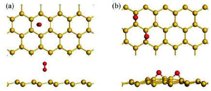
Liu et al. investigated the oxygen adsorption and dissociation on a free-standing silicene monolayerLiu . It was reported that the O2 molecule dissociates into O atoms on free-standing silicene and the formation of Si-O compound occurs. Also it was pointed out that the oxidation of silicene is easy because of the very low energy barrier for the O2 molecule to dissociate into O atoms. Depending on the initial vertical distance of the O2 molecule to the silicene layer, the resultant O atoms can bind to different sites of silicene. Among these sites the lowest energy configuration is the one for which the two O atoms reside on bridge sites of silicene (see Fig. 5(b)). The dissociation of O2 molecule on free-standing silicene is confirmed by Ozcelik et al.Ongun1 The Si-O bond lengths were calculated to be 1.71 Å and 1.73 Å for upper and lower Si atoms, respectively. The possible migration paths for an O atom from one bridge site to a neighboring bridge site exhibit energy barriers of 1.05 eV and 1.18 eV energy barriers. These are large values as compared to those for a graphene surfaceLiu . In another study, the single layer phase of silica, SiO2, was predicted as a stable honeycomblike structure by Ozcelik et al.Ongun2
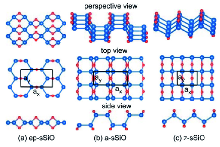
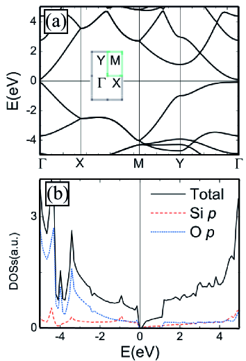
The effect of oxidation on the electronic properties of silicene was investigated by Wang et al.Wang3 They studied fully oxidized silicene with stoichiometric ratio of Si:O = 1:1. The zigzag ether-like conformation stoichiometric silicene oxide (z-sSiO) was found to be the ground state configuration (see Fig. 6(c)). The z-sSiO configuration has 14 and 165 meV/atom lower energy than the a-conformation and the ep-conformation, respectively. They reported that the z-sSiO structure is a semiconductor with a direct band gap of 0.18 eV as calculated within the GGA approximation (see Fig. 7(a)) while it is found to be 1.05 eV when the HSE06 functional is considered. In addition, Ozcelik et al. reported that single O adsorption on a silicene layer results in a direct-gap semiconducting structure with a band gap of 0.21 eVOngun1 . In the study of Ozcelik et al., the new phase of SiO2, monolayer silica, was found to be a direct-gap semiconductor with a relatively large band gap of 3.3 eV when compared to O-doped silicene layerOngun2 .
Wang et al. studied the mechanical properties of the stoichiometric SiO structure. They found that the z-sSiO monolayer has some prominent elastic characteristics, as negative Poisson ratios and exhibits an unconventional auxetic behavior. When these auxetic materials are stretched in one direction, they become thicker in the perpendicular direction. The reason for this auxetic behavior is the assembly of Si-O bonds into bending -O- network along the y-direction. The mechanical properties of monolayer silica were investigated in terms of in-plane stiffness and Poisson ratioOngun2 . It was reported that single-layer silica has an in-plane stiffness of 22.6 J/m2 which is smaller than that of graphene. Moreover, the Poisson ratio for the monolayer phase of silica was calculated to be negative like the z-sSiO monolayer. Having negative Poisson ratio is an important mechanical property for the usage of a material in biomedical and nanosensor applications.
IV HALOGENATED SILICENE
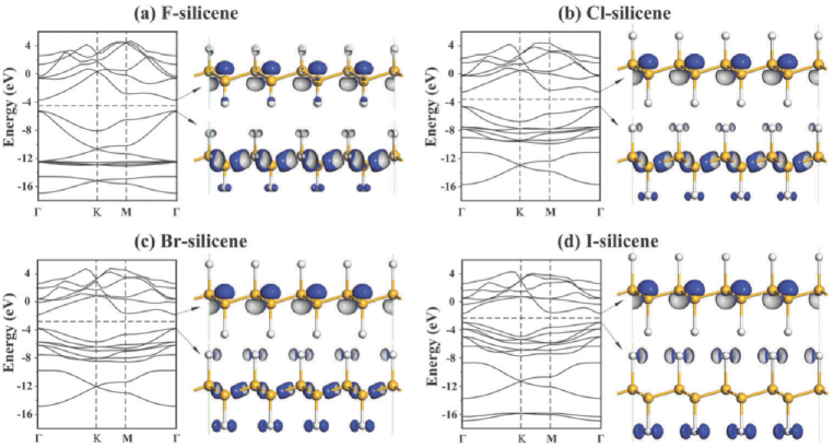
In order to integrate 2D monolayers into nanotechnological devices, fluorination and functionalization with other halogen atoms are promising methods similar to hydrogenation. Experimental and theoretical studies have shown that the band gap of fluorinated-graphene can be tuned from 0 to 5.0 eV by changing the fluorination levelcRobinson ; cSamarakoon ; cCheng1 ; cJeon ; cGarcia ; cWalter1 ; cWalter2 and half-fluorinated graphene was predicted to be magnetic.cMa Similar to the case of graphene, chemical functionalization of silicene with fluorine (F) and other halogen atoms (such as Cl, Br, and I) have also been extensively studied in the literature. Gao et al. reported that halogenation of silicene opens a band gap with various gap values depending on the atomic number of the halogen atoms.Gao The obtained band gaps are 1.19, 1.47, 1.95, and 1.98 eV for I, Br, F, and Cl atoms, respectively as shown in Fig. 8. They also reported that the formation energy increases with the increase in the atomic number of the halogen atom.
As in the hydrogenation case, several structural configurations (see Fig. 1) were also considered for the halogenation of silicene. Ding et al. studied the structural and electronic properties of fluorinated silicene alongside with hydrogenated silicene. They reported that the band gap of the boat-like (Z-line type in the corresponding study) fluorinated silicene increases almost linearly with strain, on the other hand, the band gap of the chair-like structure has a parabolic dependence around the strain value of .Ding
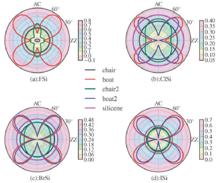
Zhang et al. investigated the geometric and the electronic structure as well as the mechanical properties of halogenated silicene XSi (X = F, Cl, Br and I) in various conformers (as shown in Fig. 1) by using first principles calculations within DFT. Their results indicated that halogenated silicene shows enhanced stability as compared with bare silicene and exhibits a tunable direct band gap.Zhang2 They reported that the chair-like structure of silicene is the most favorable one for all the halogen atoms. They also showed that, consistent with the previous resultsGao , the formation energy increases when the atomic number of the halogen atom increases which indicates that fluorination is the most favorable one among all halogenation. In addition, as shown in Fig. 9, direction dependent Poisson ratio for different conformers of the halogenated silicene were calculated and a negative Poisson ratio was predicted for the boat-like (boat2 structure in the corresponding study) structure of fluorinated siliceneZhang2 .
Moreover, Wang et al. investigated the structural, electronic and magnetic properties of half-fluorinated silicene sheets by using first principles simulation within the framework of DFT. They reported that half-fluorinated (as shown in Fig. 1) silicene sheets with zigzag, boat-like or chair-like configurations were confirmed to be dynamically stable based on phonon calculations.cWang4 Upon the adsorption of fluorine, a band gap opening is predicted in both zigzag and boat-like conformations and they were found to be direct-gap semiconductors. Moreover, half-fluorinated silicene with chair-like configuration shows antiferromagnetic ordering which is mainly induced by the unfluorinated Si atoms.
Wei et al. investigated the optical properties of fluorinated silicene by using the many-body effects by using Green’s function perturbation theory.Wei As in hydrogenation, fluorination of silicene also opens a band gap which is consistent with the previous studies. They also reported that strong excitonic effects dominate the absorption properties of hydrogenated, fluorinated silicene, and silicene nanoribbon with high exciton binding energies.
V Functionalization via Organic Molecule Adsorption
The adsorption of different chemical functional groups on silicene have potential applications for silicene-based nanoelectronic devices. Different from the highly stable planar structure of graphene, the buckled honeycomb structure of silicene leads to high chemical reactivity for functional groups. Thus, adsorption of functional groups could be a prominent method for tuning the electronic structure of silicene.
Hue et al. investigated the adsorption of NH3, NO and NO2 on silicene and found that the electronic properties of silicene are strongly depend on the type of adsorbate. Their findings revealed a significant potential of silicene for highly sensitive molecule sensors. In addition, Wen et al. found high reactivity of silicene towards NO2, O2 and SO2 molecules.Feng Binding energies of these molecules on silicene are larger than 1 eV. In contrast, the binding energies of NO and NH3 are 0.35 and 0.60 eV, respectively. While the band gap of silicene is enhanced upon adsorption of NO, O2, NH3, and SO2, it becomes half-metallic when NO2 is adsorbed. The structural and electronic properties of diverse molecules adsorbed on silicene were investigated by van der Waals included DFT.Kaloni Considered molecules are shown in Fig. 10 and their calculated adsorption energies vary from -0.11 to -0.95 eV indicating no adsorption. Moreover, electronic structure in hydrogenated silicene as well as fluorinated silicene calculations showed that the calculated band gaps range from 0.01 to 0.35 eV for acetonitrile to acetone, respectively.
Recently, Prasongkit et al. investigated the change of the electronic and transport properties when NO2, NO, NH3, and CO molecules are adsorbed onto pristine and B/N-doped silicene.Prasongkit Their results showed that NO and NO2 can be sensitively detected by pristine silicene. On the other hand, due to the weak interaction of CO and NH3 molecules with pristine silicene, the possibility of detection of those gases is relatively low. Increased sensitivity toward NH3 and CO obtained when pristine silicene is doped either by B or N atoms. Quantum conductance properties of CO molecule adsorbed silicene nanoribbons were investigated by Osborn et al.Osborn1 They showed that the quantum conduction is modified in a detectable way by weak chemisorption of a single CO molecule on a silicene nanoribbon. The adsorption of N2 and CO2 molecules do not affect the conductance. However, O2 and H2O molecules can be strongly chemisorbed and can diminish the CO detection capability of silicene. Moreover, they found that CO, O2 and H2O are easily detectable molecules among CO, CO2, O2, N2, and H2O. Gurel et al. investigated the interaction of H2, O2, CO, H2O, and OH molecules with graphene and siliceneGurel and found that H2, O2, and CO remain intact on both graphene and silicene. When these molecules adsorb at the vicinity of vacancy centers they can dissociate. The dissociations of other atoms are hindered by high energy barriers. Stephan et al. studied adsorption of benzene molecule on () silicene which was placed on the () Ag (111) surface.Stephan Their study revealed that benzene molecule can be chemisorbed on a silicene layer deposited on Ag(111) through a cycloaddition reaction. They also showed that, Si (100) and Si (111) surfaces are more reactive than the other surfaces of the structure. In addition, Stephan et al. investigated the adsorption characteristics of H2Pc molecule on silicene above Ag (111).Stephan1 They showed that, due to an electostatic or polarization repulsion between H2Pc molecule and Si surface, H2Pc molecule adopts a butterfly configuration on this surface. However, this molecule shows a planar configuration on the SiC and SiB surfaces. This study revealed the possibility of chemisorption of such large molecules on the Si/Ag system.
VI Functionalization of silicene via adatom decoration
Due to the buckled honeycomb structure of silicene, it is chemically a very active material. In order to maintain and tune its electronic properties as required, diverse growth mechanisms and various substrates were used. During growth processes the presence of foreign atoms and cluster formation is inevitable. The quality of fabricated silicene-based devices is strongly affected by the adsorbed foreign atoms. Therefore, the investigation of the decoration mechanisms of these atoms on silicene is quite essential.
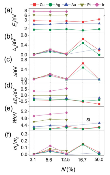
Ni et al. investigated the geometric and electronic properties of silicene with five different transition metal atoms (Cu, Ag, Au, Pt, and Ir) adsorbed at different coverages by using first principle methods.Ni Optimized geometric structures of Cu-covered silicene with different covarages are shown in Fig. 11. Similiar to Cu, favorable geometric configuration of Ag , Au, Pt, and Ir atoms is the center of silicene hegzagons. A sizable band gap can be opened without degrading the electronic properties at the Dirac point of silicene when these atoms are adsorbed. Adsorption characteristics of the metal atoms are given in Fig. 12. As shown in the figure, a band gap opening occurs in all the considered coverages and the value of the gap increases from 0.03 to 0.66 eV with increasing coverage range. Using the method of the adsorption of different transition metal atoms on different regions of silicene, they designed a silicene p-i-n tunnelling field effect transistor.
The adsorption characteristics and the stability of Li atoms on silicene was investigated by first principles calculations.Osborn2 ; Tritsaris It was reported that, Li adsorbed silicene compounds are energetically favorable and fully lithiated silicene (silicel) is the most stable form among them. The stability of the silicene sheet in the presence of completely adsorbed lithium atoms on the atom-down sites of both sides (Fig. 13) was confirmed by molecular dynamic simulations conducted at elevated temperatures. Lithiation can be used to tune the band gap of silicene and complete Li adsorption results in a band gap of 0.368 eV
Quhe et al. examined the gap opening in silicene in the presence of single-side adsorption of alkali atoms such as Li, Na, K, Rb, and Cs.Quhe They showed that the band gap of silicene can be tuned by alteration of adsorption coverage resulting in a band gap up to 0.5 eV. Moreover, quantum transport simulation of a bottom-gated FET based on a Na-covered silicene was also conducted and a transport gap with an on/off current ratio up to 108 was predicted. The electronic structure, mechanical stability, and hydrogen storage capacity of strain induced Mg functionalized silicene (SiMg) and silicane (SiHMg) monolayers have been investigated by Hussain et al.Hussain Their results revealed that high doping concentration of Mg atom can be obtained on both monolayers by biaxial symmetric strain up to 10%. The adsorption energy of H2 molecules on silicene was found to be ideal for the application in hydrogen storage devices. Li, Na, K, Be Mg and Ca adsorbed silicene sheets were studied to investigate their hydrogen-storage capacity.Hussain1 It is found that Li and Na atoms have strong metal-to-substrate binding and they are suitable for high-capacity storage of hydrogen. Using DFT calculations, the effects of an external electric field on the adsorption-desorption of H2 on a Ca-decorated silicene system was studied.Song1 Doubled binding energy enhancement is observed for H2 when 0.004 au external electric field was applied on the Ca-silicene system. On the other hand, when -0.004 au external electric field was applied to the system, the binding of 9H2 on Ca- monolayer or bilayer silicene system is getting weaker.
VII Summary
Functionalization of 2D materials is an efficient way to tailor their electronic, optical and mechanical properties. Silicene, with its highly-reactive surface structure, is a good candidate for various functionalization techniques and have been widely studied by the researchers. Recent studies have demonstrated that hydrogenation and halogenation of silicene can tune the electronic-band structure from semi-metal to semiconductor. However, by single-side adsorption of alkali atoms, Li, Na, K, Rb, and Cs, only a relatively small band gap opens. Opening a gap in silicene is rather important for its potential usage of the material in optoelectronic applications. In addition to its electronic properties, chemical functionalization of silicene can also change the Poisson ratio from positive to negative values which is important for applications in biomedicine and nanosensors. Like other 2D monolayer materials, the electronic, optical and mechanical properties of silicene could be tuned by chemical functionalization to integrate it into nanotechnological device applications.
Acknowledgements.
This work was supported by the Flemish Science Foundation (FWO-Vl) and the Methusalem foundation of the Flemish government. Computational resources were provided by TUBITAK ULAKBIM, High Performance and Grid Computing Center (TR-Grid e-Infrastructure). H.S. is supported by a FWO Pegasus Long Marie Curie Fellowship.References
- (1) —————————————–
- (2) B. C. Brodie, Phil. Trans. R. Soc. Lond. 149, 249 (1859).
- (3) R. E. Peierls, Ann. Inst. Henri Poincare 5, 177 (1935).
- (4) R. E. Peierls, Helv. Phys. Acta, 7, 81 (1934).
- (5) K. S. Novoselov, A. K. Geim, S. V. Morozov, D. Jiang, Y. Zhang, S. V. Dubonos, I. V. Grigorieva, and A. A. Firsov, Science 306, 666 (2004).
- (6) K. S. Novoselov, D. Jiang, F. Schedin, T. Booth, V. V. Khotkevich, S. Morozov, and A. K. Geim, Proc. Natl. Acad. Science U.S.A. 102, 10451 (2005).
- (7) K. S. Novoselov, A. K. Geim, S. V. Morozov, D. Jiang, M. I. Katsnelson, I. V. Grigorieva, S. V. Dubonos, and A. A. Firsov, Nature 438, 197 (2005).
- (8) H. Sahin, S. Changirov, M. Topsakal, E. Bekaroglu, E. Akturk, R. T. Senger, and S. Ciraci, Phys. Rev. B 80, 155453 (2009).
- (9) D. Golberg, Y. Bando, Y. Huang, T. Terao, M. Mitome, C. Tang, and C. Zhi, ACS Nano 4, 2979 (2010).
- (10) H. Zeng, H. Zhi, C. Zhang, Z. Wei, X. Wang, X. Guo, W. Bando, Y. Golberg, D. Nano Lett. 10, 5049 (2010).
- (11) L. Song, L. Ci, L. Lu, H. Sorokin, P. B. Jin, C. Ni, J. Kvashnin, A. G. Kvashnin, D. G. Lou, J. Yakobson, B. I. Ajayan, P. M. Nano Lett. 10, 3209 (2010).
- (12) C. Bacaksiz, H. Sahin, H. D. Ozaydin, S. Horzum, R. T. Senger, and F. M. Peeters, Phys. Rev. B 91, 085430 (2015).
- (13) H. L. Zhuang and R. G. Hennig, Appl. Phys. Lett. 101, 153109 (2012).
- (14) Q. Wang, Q. Sun, P. Jena, and Y. Kawazoe, ACS Nano 3, 621 (2009).
- (15) K. K. Kim, A. Hsu, X. Jia, S. M. Kim, Y. Shi, M. Hofmann, D. Nezich, J. F. Rodriguez-Nieva, M. Dresselhaus, T. Palacios, and J. Kong, Nano Lett. 12, 161 (2012).
- (16) M. Farahani, T. S. Ahmadi, and A. Seif, J. Mol. Struct. 913, 126 (2009).
- (17) Q. H. Wang, K. K. Zadeh, A. Kis, J. N. Coleman, and M. S. Strano, Nat. Nanotechnol. 699, 699 (2012).
- (18) J. A. Wilson and A. D. Yoffe, Adv. Phys. 18, 193 (1969).
- (19) S. Horzum, D. Cakir, J. Suh, S. Tongay, Y. S. Huang, C. H. Ho, J. Wu, H. Sahin, and F. M. Peeters, Phys. Rev. B 89, 155433 (2014).
- (20) C. Bacaksiz, S. Cahangirov, A. Rubio, R. T. Senger, F. M. Peeters, and H. Sahin, Phys. Rev. B 93, 125403 (2016).
- (21) S. Changirov, M. Topsakal, E. Akturk, H. Sahin, and S. Ciraci, Phys. Rev. B 102, 236804 (2009).
- (22) P. Vogt, P. D. Padova, C. Quaresima, J. Avila, E. Frantzeskakis, M. C. Asensio, A. Resta, B. Ealet, and G. L. Lay, Phys. Rev. Lett. 108, 155501 (2012).
- (23) C. L. Lin, R. Arafune, K. Kawahara, N. Tsukahara, E. Minamitami, Y. Kim, N. Takagi, and M. Kawai, Appl. Phys. Express 5, 045802 (2012)
- (24) A. Fleurence, R. Friedlein, T. Osaki, H. Kawai, Y. Wang, and Y. Y. Takamura, Phys. Rev. Lett. 108, 245501 (2012).
- (25) M. E. Davila, L. Xian, S. Cahangirov, A. Rubio, and G. L. Lay, New J. Phys. 16 095002 (2014).
- (26) F. F. Zhu, W. J. Chen, C. L. Gao, D. D. Guan, C. H. Liu, D. Qian, S. C. Zhang, and J. F. Jia, Nat. Mater. 14 1020 (2015).
- (27) D. W. Boukhvalov, M. I. Katsnelson, and A. I. Lichtenstein, Phys. Rev. B 77, 035427 (2008).
- (28) D. Haberer et al., Nano Lett. 10, 3360 (2010).
- (29) J. O. Sofo, A. S. Chaudhari, and G. D. Barber, Phys. Rev. B 75, 153401 (2007).
- (30) J. T. Robinson, J. S. Burgess, C. E. Junkermeier, S. C. Badescu, T. L. Reinecke, F. K. Perkins, M. K. Zalalutdniov, J. W. Baldwin, J. C. Culbertson, P. E. Sheehan, and E. S. Snow, Nano Lett. 10, 3001 (2010).
- (31) D. K. Samarakoon, Z. Chen, C. Nicolas, and X. Q. Wang, Small 7, 965 (2011).
- (32) S. H. Cheng, K. Zou, F. Okino, H. R. Gutierrez, A. Gupta, N. Shen, P. C. Eklund, J. O. Sofo, and J. Zhu, Phys. Rev. B 81, 205435 (2010).
- (33) K. J. Jeon, Z. Lee, E. Pollak, L. Moreschini, A. Bostwick, C. M. Park, R. Mendelsberg, V. Radmilovic, R. Kostecki, T. J. Richardson, and E. Rotenberg, ACS Nano 5, 1042 (2011)
- (34) J. C. Garcia, D. D. B. Lima, L. V. C. Assali, and J. F. Justo, J. Phys. Chem. C 115, 13242 (2011).
- (35) A. L. Walter, H. Sahin, K. J. Jeon, A. Bostwick, S. Horzum, R. Koch, F. Speck, M. Ostler, P. Nagel, M. Merz, S. Schupler, L. Moreschini, Y. J. Chang, T. Seyller, F. M. Peeters, K. Horn, and E. Rotenberg, ACS Nano 8, 7801 (2014).
- (36) A. L. Walter, H. Sahin, J. Kang, K. J. Jeon, A. Bostwick, S. Horzum, L. Moreschini, Y. J. Chang, F. M. Peeters, K. Horn, and E. Rotenberg, Phys. Rev. B 93, 075439 (2016).
- (37) A. Kara, H. Enriquez, A. P. Seitsonen, L. C. L. Y. Voon, S. Vizzini, B. Aufray, and H. Oughaddou, Surf. Sci. Rep. 67, 1 (2012).
- (38) M. Xu, T. Liang, M. Shi, and H. Chen, Chem. Rev. 113, 3766 (2013).
- (39) H. Sahin, J. Sivek, S. Li, B. Partoens, and F. M. Peeters Phys. Rev. B 88, 045434 (2013).
- (40) B. Lalmi, H. Oughaddou, H. Enriquez, A. Kara, S. Vizzini, B. Ealet, and B. Aufray, Appl. Phys. Lett. 97 223109 (2010).
- (41) L. Meng, Y. Wang, L. Zhang, S. Du, R. Wu, L. Li, Y. Zhang, G. Li, H. Zhou, W. A. Hofer, and H. J. Gao, Nano Lett. 13 685 (2013).
- (42) X. Lin and J. Ni, Phys. Rev. B 86, 075440 (2012).
- (43) R. Quhe, R. Fei, Q. Liu, J. Zheng, H. Li, C. Xu, Z. Ni, Y. Wang, D. Yu, Z. Gao, and J. Lu, Sci. Rep. 2, 853 (2012).
- (44) Z. Ni, H. Zhong, X. Jiang, R. Quhe, G. Luo, Y. Wang, M. Ye, J. Yang, J. Shi, and J. Lu, Nanoscale 6, 7609 (2014).
- (45) Y. C. Cheng, Z. Y. Zhu, and U. Schwingenschlogl, Europhys. Lett. 95, 17005 (2011).
- (46) J. Sivek, H. Sahin, B. Partoens, and F. M. Peeters, Phys. Rev. B 87, 085444 (2013).
- (47) R. Zheng, X. Lin, and J. Ni, Appl. Phys. Lett. 105, 092410 (2014).
- (48) H. Okamoto, Y. Sugiyama, and H. Nakano, Chem. Eur. J. 17, 9864 (2011).
- (49) H. Nakano, M. Nakano, K. Nakanishi, D. Tanaka, Y. Sugiyama, T. Ikuno, H. Okamoto, and T. Ohta, J. Amer. Chem. Soc. 134, 5452 (2012).
- (50) H. Okamoto, Y. Kumai, Y. Sugiyama, T. Mitsuoka, K. Nakanishi, T. Ohta, H. Nozaki, S. Yamaguchi, S. Shirai, and H. Nakano, J. Amer. Chem. Soc. 132, 2710 (2010).
- (51) Y. Sugiyama, H. Okamoto, T. Mitsuoka, T. Morikawa, K. Nakanishi, T. Ohta, and H. Nakano, J. Amer. Chem. Soc. 132, 5946 (2010).
- (52) P. R. Pereda and N. Takeuchi, J. of Chem. Phys. 138, 194702 (2013).
- (53) M. J. S. Spencer, M. R. Bassett, T. Morishita, I. K. Snook, and H. Nakano, New J. Phys. 15, 125018 (2013).
- (54) Y. Du, J. C. Zhuang, H. S. Liu, X. Xu, S. Eilers, K. H. Wu, C. Peng, J. J. Zhao, X. D. Pi, K. See, G. Peleckis, X. Wang, and X. Dou, ACS Nano 8, 10019 (2014).
- (55) G. Liu, M. S. Wu, C. Y. Ouyang, and B. Xu, Euro Phys. Lett. 99, 17010 (2012).
- (56) R. Qin, C. H. Wang, W. Zhu, and Y. Zhang, AIP Adv. 2, 022159 (2012).
- (57) H. Zhao, Phys. Lett. A 376, 3546 (2012).
- (58) M. Hu, X. Zhang, and D. Poulikakos, Phys. Rev. B 87, 195417 (2013).
- (59) T. P. Kaloni, Y. C. Cheng, and U. Schwingenschlögl, J. App. Phys. 113, 104305 (2013).
- (60) A.P. Durajski, D. Szczesniak, and R. Szczesniak, Solid State Comm. 200, 17 (2014).
- (61) B. Mohan, A. Kumar, and P.K. Ahluwalia, Physica E 61, 40 (2014).
- (62) T. Hussain, S. Chakraborty, A. D. Sarkar, B. Johansson, and R. Ahuja, J. App. Phys. 105, 123903 (2014).
- (63) B. Wang, J. Wu, X. Gu, H. Yin, Y. Wei, R. Yang, and M. Dresselhaus, Appl. Phys. Lett. 104, 081902 (2014).
- (64) J. Zhu and U. Schwingenschlogl, ACS Appl. Mater. Interfaces 6, 11675 (2014).
- (65) C. Yang, Z. Yu, P. Lu, Y. Liu, H. Ye, and T. Gao, Comp. Mater. Sci. 95, 420 (2014).
- (66) G. Cao and Y. Zhang, J. Cao, Phys. Lett. A 379, 1475 (2015).
- (67) Y. Ding and Y. Wang, Appl. Phys. Lett. 100, 083102 (2012).
- (68) L. C. L. Y. Voon, E. Sandberg, R. S. Aga, and A. A. Farajian, Appl. Phys. Lett. 97, 163114 (2010).
- (69) M. Houssa, E. Scalise, K. Sankaran, G. Pourtois, V. V. Afanasev, and A. Stesmans, Appl. Phys. Lett. 98, 223107 (2011).
- (70) P. Zhang, X. D. Li, C. H. Hu, S. Q. Wu, and Z. Z. Zhu, Phys. Lett. A 376, 1230 (2012).
- (71) W. Wei and T. Jacob, Phys. Rev. B 88, 045203 (2013).
- (72) N. Gao, W. T. Zheng, and Q. Jiang, Phys. Chem. Chem. Phys. 14, 257 (2012).
- (73) W. B. Zhang, Z. B. Song, and L. M. Dou, J. Mater. Chem. C 3, 3087 (2015).
- (74) X. Wang, H. Liu and S. T. Tu, RSC Adv. 36, 6238 (2015).
- (75) P. De Padova, C. Ottaviani, C. Quaresima, B. Olivieri, P. Imperatori, E. Salomon, T. Angot, L. Quagliano, C. Romano, A. Vona, M. M. Miranda, A. Generosi, B. Paci, and G. L. Lay, 2D Mater. 1, 021003 (2014).
- (76) P. De Padova, C. Quaresima, B. Olivieri, P. Perfetti, and G. L. Lay, J. Phys. D: Appl. Phys. 44, 312001 (2011).
- (77) A. Molle, C. Grazianetti, D. Chiappe, E. Cinquanta, E. Cianci, G. Tallarida, and M. Fanciulli, Adv. Func. Mater. 24, 5088 (2013).
- (78) R. Friedlein, H. V. Bui, F. B. Wiggers, Y. Y. Takamura, A. Y. Kovalgin, and M. P. de Jong, J. Chem. Phys. 140, 204705 (2014).
- (79) X. Xu, J. Zhuang, Y. Du, H. Feng, N. Zhang, C. Liu, T. Lei, J. Wang, M. Spencer, T. Morishita, X. Wang, and S. X. Dou, Sci. Rep. 4, 7543 (2014).
- (80) G. Liu, X. L. Lei, M. S. Wu, B. Xu, and C. Y. Ouyang, J. Phys. Conden. Matter. 26, 355007 (2014).
- (81) L. B. Drissi, E. H. Saidi, M. Bousmina, and O. F. Fehri, J. Phys. Conden. Matter. 24, 485502 (2012).
- (82) L. B. Drissi and F. Z. Ramadan, Physica E 68, 38 (2015).
- (83) P. Zhang, B. B. Xiao, X. L. Hou, Y. F. Zhu, and Q. Jiang, Sci. Rep. 4, 3821 (2014).
- (84) T. H. Osborn, A. A. Farajian, O. V. Pupysheva, R. S. Aga, and L.C. L. Y. Voon , Chem. Phys. Lett. 511, 101 (2011).
- (85) C. W. Zhang and S. S. Yan, J. Phys. Chem. C 116, 4163 (2012).
- (86) H. Sahin and F. M. Peeters, Phys. Rev. B 87, 085423 (2013).
- (87) K. Chinnathambi, A. Chakrabarti, A. Banerjee, and S.K. Deb, arXiv:1205.5099v1.
- (88) W. Rong, M. S. Xu, and X. D. Pi, Chinese Phys. B 24, 086807 (2015).
- (89) B. Huang, H. X. Deng, H. Lee, M. Yoon, B. G. Sumpter, F. Liu, S. C. Smith, and S. H. Wei, Phys. Rev. X 4, 021029 (2014).
- (90) Y. Liu, H. Shu, P. Liang, D. Cao, X. Chen, and W. Lu, J. Appl. Phys. 114, 094308 (2013).
- (91) P. Jamdagni, A. Kumar, M. Sharma, A. Thakur, and P. K. Ahluwalia, AIP Conf. Proc. 1661, 080007 (2015).
- (92) Q. Peng and S. De, Nanoscale 6, 1207 (2014).
- (93) C. H. Yang, Z. Y. Yu, P. F. Lu, Y. M. Liu, S. Manzoor, M. Li, and S. Zhou, Proc. SPIE 8975, 89750K-1 (2014).
- (94) Y. Wang and Y. Ding, Phys. Stat. Solidi RRL 7, 410 (2013).
- (95) V. O. Ozcelik and S. Ciraci, J. Phys. Chem. C 117, 26305 (2013).
- (96) V. O. Ozcelik, S. Cahangirov, and S. Ciraci, Phys. Rev. Lett. 112, 246803 (2014).
- (97) H. H. Gurel, V. O. Ozcelik, and S. Ciraci, J. Phys. Chem. C 118, 27574 (2014).
- (98) Y. D. Ma, Y. Dai, M. Guo, C. W. Niu, L. Yu, and B. B. Huang, Nanoscale 3, 2301 (2011).
- (99) X. Wang, H. Liu, and S. T. Tu, RSC Adv. 5, 6238 (2015).
- (100) W. Hu, N. Xia, X. Wu, Z. Li, and J. Yang, Phys. Chem. Chem. Phys. 16, 6957 (2014).
- (101) J. Wen, Y. J. Liu, H. X. Wang, J. X. Zhao, Q. H. Cai, and X. Z. Wang, Comp. Mater. Sci. 87, 218 (2014).
- (102) T. P. Kaloni, G. Schreckenbach, and M. S. Freund, J. Phys. Chem. C 118, 23361 (2014).
- (103) J. Prasongkit, R. G. Amorim, S. Chakraborty, R. Ahuja, R. H. Scheicher, and V. Amornkitbamrung, J. Phys. Chem. C 119, 16934 (2015).
- (104) T. H. Osborn and A. A. Farajian, Nano Res. 7 (7), 945 (2014).
- (105) R. Stephan, M. C. Hanf, and P. Sonnet, Phys. Chem. Chem. Phys. 17, 14495 (2015).
- (106) R. Stephan, M. C. Hanf, and P. Sonnet, J. Chem. Phys. 143, 154706 (2015).
- (107) T. H. Osborn and A. Farajian, J. Phys. Chem. C 116, 22916 (2012).
- (108) G. A. Tritsaris, E. Kaxiras, S. Meng, and E. Wang, Nano Lett. 13, 2258 (2013).
- (109) T. Hussain, S. Chakraborty, A. D. Sarkar, B. Johansson, and R. Ahuja, Appl. Phys. Lett. 105, 123903 (2014).
- (110) T. Hussain, S. Chakraborty, and R. Ahuja, Chem. Phys. Chem. Commun. 14, 3463 (2013).
- (111) E. H. Song, S. H. Yoo, J. J. Kim, S. W. Lai, Q. Jiang, and S. O. Cho, Phys. Chem. Chem. Phys. 16, 23985 (2014).