Efficient electrical spin readout of NV- centers in diamond
Abstract
Using pulsed photoionization the coherent spin manipulation and echo formation of ensembles of NV- centers in diamond are detected electrically realizing contrasts of up to . The underlying spin-dependent ionization dynamics are investigated experimentally and compared to Monte-Carlo simulations. This allows the identification of the conditions optimizing contrast and sensitivity which compare favorably with respect to optical detection.
The nitrogen vacancy center NV- in diamond is a promising candidate for quantum applications, since its coherence time at room temperature is in the range of ms Bar-Gill et al. (2013) and its spin can be read out by optical fluorescence detection Gruber et al. (1997). These features have enabled the use of NV- centers, e.g., as a quantum sensor for magnetic fields Taylor et al. (2008); Wolf et al. (2015) and temperature Acosta et al. (2010) , for scanning-probe spin imaging Maletinsky et al. (2012) and structure determination of single biological molecules Shi et al. (2015). Despite its apparent simplicity, however, optical spin readout has drawbacks: it is highly inefficient, requiring several repetitions for a single spin readout, and cumbersome to implement in many applications. Electric readout of spin in a suitable diamond semiconductor device appears as an attractive way to surmount these limitations. It could enable access to NV- centers in dense arrays, with a spacing limited by the few-nm-small feature size of electron beam lithography Manfrinato et al. (2013) rather than the optical wavelength. It might, moreover, provide a way to read out other spin defects Jungwirth et al. (2014); Christle et al. (2015); Widmann et al. (2015), potentially including optically inactive ones.
Two methods for electric readout of NV- centers have been demonstrated. The method in Ref. Brenneis et al., 2015 uses non-radiative energy transfer to graphene and detects the spin signal in the current through the graphene sheet generated by this transfer. In contrast, the method presented in Ref. Bourgeois et al., 2015 uses the charge carriers generated directly in the diamond host crystal by photoionization of the NV- centers (photocurrent detection of magnetic resonance, PDMR). Both methods, however, have until now only been used with continuous wave (cw) spin manipulation and have therefore remained limited to NV- detection. Here we demonstrate a scheme based on both pulsed spin manipulation and pulsed photoionization to truely read out the spin state of NV- centers electrically after coherent control, using Rabi oscillations and echo experiments as examples. We employ this scheme to establish a quantitative model of photoionization, simulate the readout efficiency and predict, that under optimized conditions pulsed electric readout could outperform optical fluorescence detection.
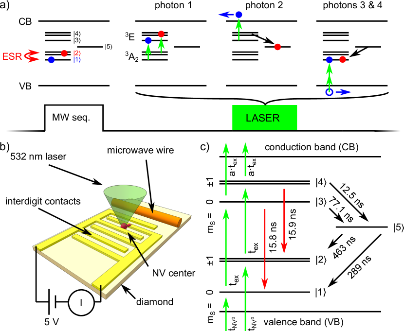
The spin-dependent photoionization cycle can be understood as an effective four-photon process, whose spin dependence relies on the NV- center’s inter-system crossing (ISC) which is also key to the classic optical readout (Fig. 1 a)) Bourgeois et al. (2015). A first photon (green arrows) triggers shelving (black arrow) of NV- centers in spin state (corresponding to the spin quantum numbers of NV-) into the long-lived metastable singlet state by this ISC. Since shelving protects this spin state from further laser excitation, absorption of a second photon preferentially ionizes NV- centers prepared in spin state (corresponding to ) into the conduction band (CB), creating a spin-dependent photocurrent (blue arrow) proportional to the population of the state obtained by a microwave pulse sequence (red arrow) preceding the optical pulse. Two further photons re-charge the NV0 center into its negative charge state by exciting the NV0 (photon 3) and capture of an electron (photon 4) from the valence band (VB) Siyushev et al. (2013).
Our spin readout experiments are performed in a photoconductor as shown in Fig. 1 b). We illuminate a densely NV--doped diamond (Element 6, grown by chemical vapor deposition, with [N] ppm, [NV] ppb) with a green laser (wavelength ) pulse generated by a Nd:YAG laser and an acousto-optic modulator (AOM) and observe the resulting photocurrent between two interdigit Schottky contacts, biased with a voltage of . The contacts (finger width , finger-to-finger distance ) consist of a 10-nm-thick titanium layer and a 80-nm-thick gold layer, deposited on the diamond surface after cleaning it in a H2SO4/H2O2 mixture, followed by an oxygen plasma treatment. The photocurrent through the sample is measured using a transimpedance amplifier (amplification , bandwidth ). Depending on the measurement we use a x, a x or a x objective, with numeric apertures of , and and diffraction limited spot sizes of , and , resp.The microwave with frequency for spin manipulation is delivered to the sample using a wire next to the interdigit contact structure (cf. Fig. 1 b)).

We first demonstrate that coherent control of the NV- centers can be detected electrically using the pulse sequence shown on top of Fig. 2 a) and b). To excite electron spin resonance (ESR) transitions, the sequence starts with a microwave pulse with power and varying duration . This initializes the spin of the NV- 3A2 ground state. After a brief delay an optical excitation pulse follows (x objective, light power of during the optical pulse). Furthermore, an external magnetic field of is applied to the sample parallel to one of the \hkl111 axes via a permanent magnet so that only one crystallographic NV- direction can be addressed. Figure 2 a) shows the pulsed electrically detected magnetic resonance (pEDMR) spectrum obtained under these conditions, monitoring the dc current through the interdigit contact structure. In contrast to previous pEDMR experiments on silicon and organic semiconductors, where the spin dependence of comparatively slow recombination or hopping processes is monitored via a boxcar integration of the current transients following the spin manipulation Boehme and Lips (2003); Stegner et al. (2006); Harneit et al. (2007); Hoehne et al. (2013); Kupijai et al. (2015), the much faster pulse sequence repetition possible due to the fast photoioniziation and spin state initialization allows this vastly simpler direct detection of the spin signal in the dc current. As an example, the pulse repetition time is in Fig. 2 a). On a background photocurrent level of resonant decreases of the photocurrent are observed at and , corresponding to one \hkl111 orientation parallel to the field and three off-axis \hkl111 orientations, resp. The resonant change of the current of at corresponds to a relative spin-dependent current change (contrast) of .
Rabi oscillations are observed when the length of the microwave pulse is changed, adjusting the waiting time to keep constant at . Figure 2 b) shows the expected oscillatory dependence of on . That indeed Rabi oscillations are obtained is demonstrated in the inset of Fig. 2 b), where the characteristic linear dependence of the oscillation frequency on and, therefore, on the microwave magnetic field is observed. The Rabi oscillations exhibit an effective dephasing time of , in accordance with other results on diamond with neutral isotope composition Parker et al. (2015); Mizuochi et al. (2009). In all experiments represented in Fig. 2 b) to d) was determined by cycling the microwave frequency between the resonant and two nonresonant frequencies and , resulting in a low-frequency lock-in amplification Hoehne et al. (2012).
The pulsed electrical detection scheme developed here also allows to detect spin echos, e.g., by using the pulse sequence depicted on top of Fig. 2 c) and d). As in the case of optically detected magnetic resonance (ODMR) Breiland et al. (1973); Childress et al. (2006) and other pEDMR Huebl et al. (2008) experiments, the corresponding Hahn echo sequence needs to be extended by a final pulse, which projects the coherence echo to a polarisation accessible to optical or electrical readout. Figure 2 c) shows the echo in the contrast as a function of for a fixed . At the total microwave pulse applied equals a nutation of , so that the contrast is minimal, in full agreement with Fig. 2 b). For significantly smaller or longer than , no coherence echo is formed and the final projection pulse leads to an equal distribution of spin states which favor or which do not favor photoionization Huebl et al. (2008); Franke et al. (2014). Indeed, a maximum of is observed for or , in reasonable agreement with the contrast for pulses found in the Rabi oscillation experiment.
Finally, these echo experiments can also be performed as a function of total evolution time with , giving access, e.g., to decoherence and to weak hyperfine interaction via electron spin echo envelope modulation (ESEEM). Figure 2 d) shows such an echo decay experiment on the resonance where the decay is caused by ESEEM Stanwix et al. (2010). Again, the pulse sequence repetition time is kept constant, the long times necessary for this experiment reduce the signal-to-noise ratio. Nevertheless, the experiments summarized in Fig. 2 clearly demonstrate that all fundamental coherent experiments can be performed on the NV- center with the electrical readout scheme developed here.
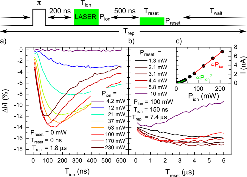
We now turn to study the readout contrast that can be obtained by pulsed electric readout. We therefore place ourselves at , where all four NV- orientations merge into a single resonance at , and where we can essentially flip NV- with all orientations into state by a microwave pulse of length using . Under these conditions we study the readout contrast as a function of both the duration and intensity of the readout light pulse (Fig. 3 top), keeping illumination as homogeneous as possible by widening the laser beam with the x objective to a spot size of .
Figure 3 a) plots versus for different . For each power we find an optimum pulse length between a regime of too short pulses, where the ionization of NV- mostly takes place on a timescale faster than the shelving process suppressing the spin selection via the ISC, and too long pulses, where mostly NV- contribute to the current which have lost their spin information by a decay through the ISC or by a preceding ionization. Optimizing and for the sample studied, we reach an optimum contrast of at an intermediate power of . As will be discussed below, this value is probably limited by ionization of background substitutional nitrogen donors () Bourgeois et al. (2015, 2016).
The pulse powers and lengths optimal for readout may not be optimal for initialization and conversion of NV0 to NV-. Therefore in Fig. 3 b) we introduce a second laser pulse to separate the ionization process from the NV- initialization. Here is plotted against the reset pulse length for different reset pulse powers . Small reset pulse powers improve for increasing . The optimal leads to a maximal of which is reached for longer than . For higher the reset pulse itself starts to ionize the NV- centers which leads to a decrease of since the NV- have already undergone spin-dependent ionization or a decay through the ISC which eradicates all spin information.
We can quantitatively reproduce these observations by a Monte-Carlo model of the NV- center’s optical cycle together with photoionization and recharging of the NV0 (Fig. 1 c)) using the partial lifetimes of Ref. Robledo et al., 2011. The excitation time from the 3A2 ground state of the NV- to its 3E excited state, the characteristic time of the ionization process and the lifetime of the ionized state are used as parameters in the simulation. The simulation is repeated million times for each starting state. Whenever the simulation transitions from NV- to NV0 or from NV0 to NV-, the generation of an electron or a hole in the respective bands at that time is recorded. Following the treatment in Ref. Rose, 1963 the photocurrent through the diamond sample is , with the elemental charge , the charge carrier generation rate , the typical charge carrier lifetime and the typical transit time of the charge carriers through the photoconductor device. The ratio of and is called the photoconductive gain , so that . Since the charge carrier generation rate is not constant throughout the measurement we replace by its mean with the number of charge carriers generated during the laser pulse time . To account for a background current , originating from the ionization of , we add the generation of electrons with a rate which allows to parametrize its dependence on the optical power. Microwave pulse imperfections yielding a mixture between and at the start of the experiment are described by a parameter multiplied with the contrast curve. The contrast then becomes
| (1) |
where the subscript or denotes the respective value for the initial states and .
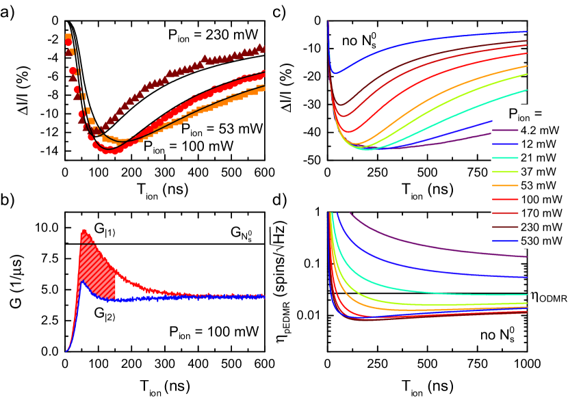
This term is fitted simultaneously to the data presented in Fig. 3 for the three laser powers of , and using the Nelder-Mead simplex algorithm. The fit parameters , , and are used globally for all fits while is scaled according to the laser power used in the different experiments. To keep the complexity of the simulation down we use only one for all three fits which overestimates the generated photocurrent for small laser powers and vice versa. Figure 4 a) compares and the fit of the Monte-Carlo simulation, which are in very good agreement. We find , , , and . A in the range of tens of is in agreement with the onset of a saturation in the photocurrent at (cf. Fig. 3 c)) which we expect to happen at the point where the excitation time from to reaches the partial lifetime for the states to the state . is probably caused by the limited pulse fidelity at , since differently oriented NV- centers have different Rabi frequencies.
The model and the parameters determined allow us to simulate the charge carrier generation dynamics in our sample during a laser pulse. Figure 4 b) shows the charge carrier generation rate and for . The horizontal line depicts a background current originating from at . For times bigger than all spin-dependent signal is lost and the system is in a steady state with , each at about the charge carrier generation rate originating from . For pulsed illumination with a pulse length we find , and an background of by integration over the curves. Therefore, even at high laser powers, the contrast is limited by ionization.
In order to find the limits of our detection method in samples free of background we simulate without a background photocurrent, with instantaneous AOM turn-on, and with . Figure 4 c) plots the contrast simulated under these conditions versus . Again, the has an optimal for each . The most notable difference is the maximal contrast of which is predicted for a laser power of .
However, we expect maximum sensitivity to be obtained for rather different optical pulse conditions. A sensitivity is usually defined by , with SNR the signal-to-noise ratio, the number of spins and the detection bandwidth of the particular experiment Boero et al. (2003). For ODMR we find the SNR using Poissonian statistics where the difference in photoluminescene (PL) counts for the different initial states is divided by the shot noise generated by the number of counts of the bright initial state . For pEDMR we use the difference in the current divided by the sum of the shot noise generated by the total current Müller (1990) and the amplifier input noise . With this we find
| (2) | ||||
| (3) |
where the subscript single denotes the corresponding value for a single NV- center and is the contrast of the corresponding measurement. Figure 4 d) plots the simulated sensitivity at a sequence repetition rate of and for a typical amplifier input noise of versus . For each the sensitivity decreases (i.e. improves) with longer because of the increased current and contrast for longer ionization pulse times. After reaching an optimal value increases again since the decrease in contrast cancels the effects of the higher currents. The expected optimal sensitivity of for pEDMR is not reached for the laser power corresponding to the maximum contrast but rather for between and and . For comparison, the sensitivity for a typical ODMR experiment on a single NV- center with a countrate of , a contrast of and an integration time over the fluorescence of is which is marked by the black horizontal line in Fig. 4 d).
To put this sensitivity in absolute numbers: Using a x objective and of laser power a cw photocurrent of is generated in our sample. Comparing the PL observed on it and on a reference sample with single NV- centers allows us to estimate the number of NV- participating to about so that each NV- contributes a photocurrent of . Simulations under the corresponding power of for the x objective predict a current of per NV-, so that the photoconductive gain in our samples is as expected for a metal-semiconductor-metal photodetector based on Schottky contacts. Under the optimized conditions given above ( optical power for a x objective, repetition rate, , , no background current, no pulse imperfections), a single NV- should exhibit a on a photocurrent of , which should be easily measurable. This corresponds to a ’count rate’ of elementary charges at a spin contrast of , numbers which are not reached for photons in conventional detection setups
In summary, using a combination of pulsed photoionization and pulsed spin manipulation, we have demonstrated electrical readout of the coherent control of an ensemble of NV- centers. With the help of a Monte-Carlo simulation we have improved our understanding of the photoionization dynamics and find that single-spin (multi-shot) detection should be feasible electrically, possibly with a higher sensitivity than optically. These results motivate a range of further studies, in particular into the relative benefits of photoconductors with ohmic or Schottky contacts and into more advanced photoionization schemes using lasers with different photon energies Shields et al. (2015); Hopper et al. (2016); Bourgeois et al. (2016), which could lead to higher ionization efficiencies and a better understanding of the dynamics. Furthermore, EDMR based on photoionization should be transferable to other defects and other host materials such as SiC, which might allow even easier integration of electrical spin readout, e.g., with bipolar device structures.
This work was supported financially by Deutsche Forschungsgemeinschaft via FOR 1493 (STU139/11-2), SPP 1601 (BR 1585/8-2) and Emmy Noether grant RE 3606/1-1.
References
- Bar-Gill et al. (2013) N. Bar-Gill, L. M. Pham, A. Jarmola, D. Budker, and R. L. Walsworth, Nature Communications 4, 1743 (2013).
- Gruber et al. (1997) A. Gruber, A. Dräbenstedt, C. Tietz, L. Fleury, J. Wrachtrup, and C. v. Borczyskowski, Science 276, 2012 (1997).
- Taylor et al. (2008) J. M. Taylor, P. Cappellaro, L. Childress, L. Jiang, D. Budker, P. R. Hemmer, A. Yacoby, R. Walsworth, and M. D. Lukin, Nature Physics 4, 810 (2008).
- Wolf et al. (2015) T. Wolf, P. Neumann, K. Nakamura, H. Sumiya, T. Ohshima, J. Isoya, and J. Wrachtrup, Physical Review X 5, 041001 (2015).
- Acosta et al. (2010) V. M. Acosta, E. Bauch, M. P. Ledbetter, A. Waxman, L.-S. Bouchard, and D. Budker, Physical Review Letters 104, 070801 (2010).
- Maletinsky et al. (2012) P. Maletinsky, S. S. Hong, M. Grinolds, B. Hausmann, M. D. Lukin, R. L. Walsworth, M. Loncar, and A. Yacoby, Nature Nanotechnology 7, 320 (2012).
- Shi et al. (2015) F. Shi, Q. Zhang, P. Wang, H. Sun, J. Wang, X. Rong, M. Chen, C. Ju, F. Reinhard, H. Chen, J. Wrachtrup, J. Wang, and J. Du, Science 347, 1135 (2015).
- Manfrinato et al. (2013) V. R. Manfrinato, L. Zhang, D. Su, H. Duan, R. G. Hobbs, E. A. Stach, and K. K. Berggren, Nano Letters 13, 1555 (2013).
- Jungwirth et al. (2014) N. R. Jungwirth, Y. Y. Pai, H. S. Chang, E. R. MacQuarrie, K. X. Nguyen, and G. D. Fuchs, Journal of Applied Physics 116, 043509 (2014).
- Christle et al. (2015) D. J. Christle, A. L. Falk, P. Andrich, P. V. Klimov, J. U. Hassan, N. T. Son, E. Janzén, T. Ohshima, and D. D. Awschalom, Nature Materials 14, 160 (2015).
- Widmann et al. (2015) M. Widmann, S.-Y. Lee, T. Rendler, N. T. Son, H. Fedder, S. Paik, L.-P. Yang, N. Zhao, S. Yang, I. Booker, A. Denisenko, M. Jamali, S. A. Momenzadeh, I. Gerhardt, T. Ohshima, A. Gali, E. Janzén, and J. Wrachtrup, Nature Materials 14, 164 (2015).
- Brenneis et al. (2015) A. Brenneis, L. Gaudreau, M. Seifert, H. Karl, M. S. Brandt, H. Huebl, J. A. Garrido, F. H. L. Koppens, and A. W. Holleitner, Nature Nanotechnology 10, 135 (2015).
- Bourgeois et al. (2015) E. Bourgeois, A. Jarmola, P. Siyushev, M. Gulka, J. Hruby, F. Jelezko, D. Budker, and M. Nesladek, Nature Communications 6, 8577 (2015).
- Siyushev et al. (2013) P. Siyushev, H. Pinto, M. Vörös, A. Gali, F. Jelezko, and J. Wrachtrup, Physical Review Letters 110, 167402 (2013).
- Boehme and Lips (2003) C. Boehme and K. Lips, Physical Review B 68, 245105 (2003).
- Stegner et al. (2006) A. R. Stegner, C. Boehme, H. Huebl, M. Stutzmann, K. Lips, and M. S. Brandt, Nature Physics 2, 835 (2006).
- Harneit et al. (2007) W. Harneit, C. Boehme, S. Schaefer, K. Huebener, K. Fostiropoulos, and K. Lips, Physical Review Letters 98, 216601 (2007).
- Hoehne et al. (2013) F. Hoehne, L. Dreher, M. Suckert, D. P. Franke, M. Stutzmann, and M. S. Brandt, Physical Review B 88, 155301 (2013).
- Kupijai et al. (2015) A. J. Kupijai, K. M. Behringer, F. G. Schaeble, N. E. Galfe, M. Corazza, S. A. Gevorgyan, F. C. Krebs, M. Stutzmann, and M. S. Brandt, Physical Review B 92, 245203 (2015).
- Parker et al. (2015) A. J. Parker, H.-J. Wang, Y. Li, A. Pines, and J. P. King, arXiv:1506.05484 (2015).
- Mizuochi et al. (2009) N. Mizuochi, P. Neumann, F. Rempp, J. Beck, V. Jacques, P. Siyushev, K. Nakamura, D. J. Twitchen, H. Watanabe, S. Yamasaki, F. Jelezko, and J. Wrachtrup, Physical Review B 80, 041201 (2009).
- Hoehne et al. (2012) F. Hoehne, L. Dreher, J. Behrends, M. Fehr, H. Huebl, K. Lips, A. Schnegg, M. Suckert, M. Stutzmann, and M. S. Brandt, Review of Scientific Instruments 83, 043907 (2012).
- Breiland et al. (1973) W. G. Breiland, C. B. Harris, and A. Pines, Physical Review Letters 30, 158 (1973).
- Childress et al. (2006) L. Childress, M. V. G. Dutt, J. M. Taylor, A. S. Zibrov, F. Jelezko, J. Wrachtrup, P. R. Hemmer, and M. D. Lukin, Science 314, 281 (2006).
- Huebl et al. (2008) H. Huebl, F. Hoehne, B. Grolik, A. R. Stegner, M. Stutzmann, and M. S. Brandt, Physical Review Letters 100, 177602 (2008).
- Franke et al. (2014) D. P. Franke, F. Hoehne, L. S. Vlasenko, K. M. Itoh, and M. S. Brandt, Physical Review B 89, 195207 (2014).
- Stanwix et al. (2010) P. L. Stanwix, L. M. Pham, J. R. Maze, D. Le Sage, T. K. Yeung, P. Cappellaro, P. R. Hemmer, A. Yacoby, M. D. Lukin, and R. L. Walsworth, Physical Review B 82, 201201 (2010).
- Bourgeois et al. (2016) E. Bourgeois, E. Londero, K. Buczak, Y. Balasubramaniam, G. Wachter, J. Stursa, K. Dobes, F. Aumayr, M. Trupke, A. Gali, and M. Nesladek, arXiv:1607.00961 (2016).
- Robledo et al. (2011) L. Robledo, H. Bernien, T. v. d. Sar, and R. Hanson, New Journal of Physics 13, 025013 (2011).
- Rose (1963) A. Rose, Concepts in Photoconductivity and Allied Problems (Interscience Publishers, New York, 1963).
- Boero et al. (2003) G. Boero, M. Bouterfas, C. Massin, F. Vincent, P.-A. Besse, R. S. Popovic, and A. Schweiger, Review of Scientific Instruments 74, 4794 (2003).
- Müller (1990) R. Müller, Rauschen (Springer Verlag, Berlin, 1990).
- Shields et al. (2015) B. Shields, Q. Unterreithmeier, N. de Leon, H. Park, and M. Lukin, Physical Review Letters 114, 136402 (2015).
- Hopper et al. (2016) D. A. Hopper, R. R. Grote, A. L. Exarhos, and L. C. Bassett, arXiv:1606.06600 (2016).