Effect of valence fluctuations on the ground state properties of SmB6
Abstract
We argue that because of valence-fluctuation caused dynamical changes (fluctuations) of impurity energies in the impurity band of SmB6,
energies of electrons occupying impurity sites can be due to the uncertainty principle only estimated with corresponding uncertainty,
so they can be represented by energy intervals of non-zero width.
As a consequence, both occupied as well as unoccupied states can be found in the impurity band
above as well as below Fermi level even in the ground state.
Therefore the subsystem of localized charge carriers in the ground state of SmB6 cannot be described
by an energy distribution function expected for K. This fundamental conclusion adds another reason
for absence of resistivity divergence in SmB6 at lowest temperatures,
and sheds new light on interpretation of experimental data obtained for SmB6 and similar systems
at lowest temperatures.
Keywords: A. SmB6; A. Kondo Insulators; D. Valence Fluctuations
SmB6 is a prototypical mixed valence material revealing properties of a narrow-gap semiconductor down to temperatures of a few Kelvin [1, 2, 3, 4]. Paradoxically, at lowest temperatures it exhibits metallic-like conductivity, which is moreover smaller than the Mott’s minimum metallic conductivity [1, 2, 3]. Such temperature non-activated electrical transport of SmB6 at lowest temperatures cannot be attributed to any scattering scenario known for metals, because extremely high value of the residual resistivity would unconditionally require superunitary scattering with unphysical concentration of scattering centers [1, 2, 3], at least 80 per unit cell [3]. This fundamental discrepancy between theory and experiment is a subject of long-standing controversy precluding to conclude whether ground state of SmB6 is metallic, or insulating. In fact, according to Mott-Ioffe-Regel viewpoint conventional Boltzmann transport theory becomes meaningless if the characteristic mean free path of the itinerant conduction electrons becomes comparable to, or less than the interatomic spacing [5, 6, 7, 8]. Therefore the requirement for superunitary scattering implicates that either (i) electrical conductivity is not homogeneous in the volume, i.e. material contains metallic regions forming a conductive path along the sample that is responsible for electrical conductivity at lowest temperatures [9, 10, 11, 12, 13] or (ii) electrical transport at lowest temperatures is realized via a hopping process, which however, has to be temperature non-activated [14].
The first mentioned approach is represented by scenarios supposing metallic surface in SmB6 that could be either of topological nature [9, 10, 11, 12] or due to ”trivial” polarity-driven surface states [13]. Several experimental observations indicate metallic surface transport in SmB6 [15, 16, 17] while there exists huge research effort to prove the existence of topologically protected surface states [18, 19, 20, 21, 22, 23, 24, 25]. On the other hand, latest developments provide also evidence of trivial surface states in SmB6 [26]. It has been also suggested that only the most stoichiometric SmB6 samples possess a bulk gap necessary for the topological Kondo insulator state [27]. However, up to now, convincing conclusion about the nature of metallic surface states in SmB6 is still missing.
The second mentioned approach is represented by a recently proposed model of valence-fluctuation induced hopping transport [14]. The model is based on the fact that valence fluctuations (VFs) of Sm ions are intrinsically accompanied by fluctuations of charge, ionic radii and magnetic moments of Sm ions, what unconditionally causes fluctuations of the energies of impurities in the impurity band of SmB6. As a consequence there are created favorable conditions for temperature non-activated hops (as in more details summarized below), resulting in temperature non-activated hopping transport [14]. The model intrinsically infers an enhanced conductivity of the surface layer because of higher concentration of lattice imperfections [14], thus resembling a characteristic property of topological insulators [14]. In association with this it should be emphasized here that although the scenario as presented in our previous work [14] has a capability to explain properties of SmB6 without necessity to consider Kondo topological insulator (KTI) scenario, it does not exclude a possibility of existence of topologically protected surface states in SmB6. In fact, both of them can coexist, thus their features can be ”mixed” in SmB6.
The purpose of this work is to point out that besides valence-fluctuation induced hopping transport as proposed before [14], another consequence of dynamical changes of the energies of impurities in SmB6 due to VFs is that the energy distribution function of the charge carrier subsystem in the ground state corresponds to presence of occupied states above Fermi level and empty ones below Fermi level, thus resembling effect of thermal broadening. This implicates that temperature of charge carrier subsystem in the ground state of SmB6 cannot be K.
For convenience of further discussion let us first recapitulate essential ideas of the original model of valence-fluctuation induced hopping transport [14]. In a semiconductor with an impurity band (IB) that contains metallic ions in two different valency states, say and , energy of an impurity is affected by (re)distribution of and ions in its vicinity (because of different interaction energy between the impurity and / ion due to different charge, ionic radii, and magnetic moment) [14]. Considering a hypothetical rearrangement process (RP) causing repetitious changes in distribution of and ions on metal ion positions with a characteristic time constant, , this RP unconditionally causes also repetitive changes of the energies of impurities with the same characteristic time constant [14]. Therefore, the energy of the impurity in the impurity band is not constant in time, but varies within the interval [14].
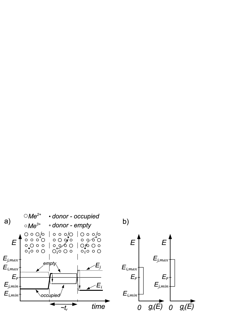
Assuming that Fermi level, , lies in the IB formed by one type of impurities (e.g. donors) and is characterized by a constant density of states (DOS), , and supposing that dynamical changes of the impurity energies are adequately characterized by a typical width of the energy interval , then there must exist a subnetwork of impurities with energy satisfying the condition [14]
| (1) |
The concentration of impurities in this subnetwork is , thus a typical distance between two nearest impurities is [14]. The impurities defined by the inequality (1) have a unique property: rearrangements of ions in the vicinity of these impurities cause that some occupied impurity energy levels can shift from the region below to the region above , and analogously, some empty ones from the region above can shift under [14]. Such processes, driven by the RP create favorable conditions for electron hops (tunneling) to empty sites of lower energy, i.e. hops with zero activation energy, as depicted in Fig. 1. It was shown [14] that probability of RP-induced hops, , at sufficiently low temperatures can be expressed as , where is a localization length, and is defined as the time-averaged probability per unit volume that for a temporarily occupied site belonging to the subnetwork defined by the inequality (1) there will appear an empty state of lower energy in the subnetwork as a consequence of the RP. Accepting the fact that valence fluctuations (VFs) represent a special case of the RP, probability of valence-fluctuation induced hop, can be expressed as
| (2) |
where is defined analogously as [14]. Direct consequence of Eq. (2) is that hopping probability exponentially increases with decrease of hop distance , what implicates an enhanced conductivity in the vicinity of the surface because of higher concentration of lattice imperfections which can play role of hopping centers [14].
Now let us focus on another fundamental impact of the RP. Due to the RP energy levels of impurities defined by the inequality (1) repetitively pass through the Fermi level, resulting in possible temperature non-activated electron hops, as depicted in Fig. 1. In the simplest case, when is of the order of the Debye energy or smaller, and is small compared to , the intrinsic transition rate for an electron hopping from a site with energy to an empty site with energy is well approximated by the “quantum-limit” hopping formula [28]
| (3) | |||
| (4) |
where is Boltzmann constant, is the distance between sites and , and is some constant, which depends on the electron-phonon coupling strength, the phonon density of states, and other properties of the material, but which depends only weakly on the energies and or on [28]. According to Eq. (4), the intrinsic transition rate of the electron hopping to a site of less energy decreases exponentially with increasing . Because is finite, must be also finite, so there is always non-zero time interval until an electron can hop (tunnel) to some empty site of less energy, while this time interval increases with increasing distance between sites. Therefore, if the RP is a ground state property of a material, finite implicates a non-zero probability of finding some occupied energy levels above in the ground state. Neglecting electron-electron interactions except that not more than one electron can occupy a single site, time averaged occupation number of site in thermal equilibrium can be expressed in form [28], what for K unconditionally requires that all sites having energy below are occupied and all sites having energy above are empty. Therefore, if there exist some occupied sites with energy levels above in the ground state of a material with the RP, then the charge carrier subsystem in the ground state of this material can not be at absolute zero.
Because VFs can be regarded as a special case of the RP, analogous scenario as indicated above can be expected in valence fluctuating semiconductors, too. In principle, VFs are RPs with a short characteristic time constant . However, according to Heisenberg relation if is short enough, uncertainty of energy of the electron occupying site () may cause situation that energy of the electron occupying site becomes indistinguishable from the energy of empty site , to which the electron ”is going” to hop. This limit case has no essential impact on the valence-fluctuation induced hopping transport as proposed before [14], such as hops between sites and with indistinguishable energies can also be treated as hops/tunneling not requiring thermal activation, however, it becomes crucial in discussion on possible effect of VFs on the energy distribution function of localized charge carriers in the ground state of valence fluctuating materials, such as SmB6.
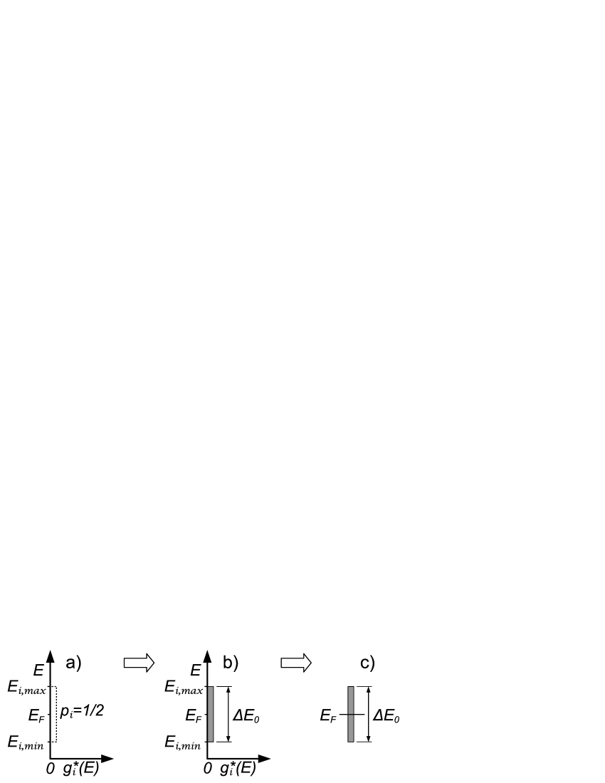
The charge fluctuation rate in SmB6 estimated from phonon spectroscopy studies [29, 30] is 200 cm-1 650 cm-1, what corresponds to the characteristic time (which defines time changes of the impurity energy due to changes of the Coulomb interaction between the impurity and the surrounding Sm2+/Sm3+ ions) of s 1.7 s. According to Heisenberg relation the uncertainty of the energy of electron occupying the impurity site can be estimated as , what yields for SmB6 between 4 meV and 13 meV. Because energies of the impurities fluctuating within the interval of lie in the impurity band of the width that is located in the forbidden gap of the width , the inequality is satisfied. The value of detected by many experimental techniques is between 2 and 20 meV in SmB6 [31, 1, 2, 32, 33, 34, 35, 3, 36, 37, 38, 4, 39], what can be an indication that the above estimated uncertainty of the energy of electron occupying an impurity site () is greater or comparable with the width of the impurity band (). Based on this we suppose that the whole interval in which the energy of impurity fluctuates (because of fluctuations of local physical parameters which affect its energy) defines at the same time the energy uncertainty of electron occupying the impurity site (as a consequence of a characteristic time of fluctuations and uncertainty principle). Taking into account this supposition we present energy diagram model of impurity sites in SmB6 as follows.
Let us associate hopping sites in SmB6 with donor-type impurity states having fluctuating energy levels lying in the impurity band of SmB6. Each hopping site is characterized by energy interval of the width defining energy broadening/uncertainty of this site. Thus we treat the hopping center as a narrow band of the energy width , and we denote it as uncertainty band of the impurity energy (UBIE). The UBIE of a site is defined by the partial DOS, , which is non-zero and constant within the energy interval and zero outside it, and by a time averaged probability of the occupation of site by an electron, , as depicted in Fig. 2a. Expressing using a color scale the UBIE can be depicted as done in Fig. 2b, or in the most simplified form in Fig. 2c.
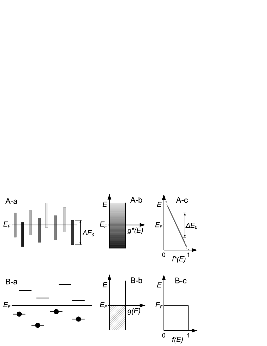
How the situation in the impurity band of SmB6 in very close vicinity of the Fermi level can look like show illustrations in Fig. 3A. Here the hopping sites are represented by UBIEs crossing the Fermi level (), and the partial DOS of the individual impurity, , is shown as a bar of corresponding dimensions and position in the energy scale (see Fig. 3A-a). We consider that all UBIEs have identical properties except their position in energy scale, and that their distribution in the impurity band of SmB6 is uniform. Thus, the total DOS, , being a sum of all partial DOS of individual impurity states, , is constant (see Fig. 3A-b). The time averaged probability of the occupation of site by an electron, , we define as the average value of the function over the energy interval . At such conditions, for the UBIE centered at the Fermi level and decreases/increases at increasing/decreasing (and ). The time averaged probability of occupation of the state at energy in the impurity band, , can be determined as average value of of all UBIEs with non-zero . The behavior of , qualitatively depicted in Fig. 3A-c (and also visualized by color representation in Fig. 3A-b) is a continuous function of energy in a close vicinity of the Fermi level, having a finite slope at the Fermi level. This ”energy broadening” of having its origin in VFs cannot be less than broadening/uncertainty introduced by VFs (expressed by the width of UBIEs, ). An important point is that energy broadening induced by VFs will take place in SmB6 also in the case if no thermal broadening can be expected This is a fundamental difference in comparison to a classic semiconductor at K (see Fig. 3B), where all impurity energy levels below the Fermi level are occupied and all ones above the Fermi level are empty (as depicted in Fig. 3B-a and Fig. 3B-b), so the energy distribution function, , is a step function (as depicted in Fig. 3B-c).
Now let us consider an imaginary experiment. Let SmB6 sample is in ideal thermal contact with a thermal reservoir at absolute zero, so the charge carrier subsystem of SmB6 has to be in the ground state. Supposing presence of VFs in the ground state of SmB6, the charge carrier subsystem in the ground state of SmB6 will be characterized by monotonic and continuous function of energy in a close vicinity of the Fermi level, like shown in Fig. 3A-c. If energy distribution function of the charge carrier subsystem (being in thermal equilibrium, and in absence of electrical field) can be approximated by Fermi-Dirac distribution function, at lowest temperatures, then the energy distribution function of charge carriers in the ground state of SmB6 can be approximated by , where represents the temperature of the charge carrier subsystem in the ground state. Essential point is that has to be non-zero, such as zero value of would require that is a step function, what as follows from the discussion above cannot be the case in SmB6. It can be therefore concluded that temperature of charge carrier subsystem in the ground state of SmB6 cannot be zero, thus neither the electrical conductivity of SmB6 in the ground state can be zero, such as zero electrical conductivity is the property of a semiconductor with hopping conduction only at K. Consequently, although the SmB6 sample is in ideal thermal contact with a thermal reservoir, which is at temperature , physical properties of SmB6 that are governed by energy distribution function of charge carrier subsystem will reveal only negligible dependence on the temperature of the thermal reservoir, while a ”crossover” to this regime will be observed at temperatures of thermal reservoir comparable with .
With regard to the discussion in the paragraph above it is worthy to mention that detailed resistivity studies of SmB6 down to 15 mK reported by Kasuya and coworkers [2] have shown that the best fit of their experimental data down to 100 mK is represented by the formula [cm-1], while the resistivity is nearly constant below 100 mK. Surprisingly, such fit corresponds to Arrhenius-type activation process with “shift” in temperature scale by 4,87 K. If we associate this temperature shift with the non-zero temperature of charge carriers in the ground state of SmB6, K, Kasuya’s result can be interpreted by means that at cooling SmB6 sample, when temperature of the cooling system (thermal reservoir) approaches absolute zero the sample conductivity approaches the value expected for Arrhenius-type activation process at temperature of charge carriers of K. In addition, such estimated yields surprisingly good correspondence with the fact that plateau in the dc resistivity temperature dependence of SmB6 samples of various qualities is observed below 5 K [1, 2, 3, 36, 4, 15, 16, 23, 25, 17, 31, 38].
In association with impact of VFs on the ground state properties of charge carrier subsystem in SmB6 it should be also emphasized that valence fluctuations of Sm ions are associated with fluctuations of their ionic radii, consequently causing corresponding lattice vibrations. In a ”classic” crystal lattice at absolute zero there are no phonons [40], so here arises a question about energy distribution function of phonons, which assist to VFs in the ground state of SmB6. A non-zero thermal coupling between the lattice and charge carrier subsystem having a non-zero temperature in the ground state implicates a non-zero ground state temperature of the phonon subsystem, too. However, discussion of this issue is beyond the scope of this paper.
It can be concluded that discussed effect of valence fluctuations on the energy distribution function of localized charge carriers yields alternative explanation for the resistivity saturation in SmB6 at lowest temperatures, while one does not exclude possibility of existence of metallic surface states in this material (e.g. topologically protected [9, 10, 11, 12] or polarity-driven ”trivial” surface states [13]). Moreover, this effect allows us to explain also the ground state properties of nonstoichiometric SmB6 samples. It would be worthy to emphasize here that it was recently suggested that the presence of even 1 % of Sm vacancies leads to a smearing of the bulk hybridization gap in SmB6 samples and would result in a breakdown of the KTI state [27]. Thus, only the most stoichiometric SmB6 samples possess a bulk gap necessary for the topological Kondo insulator state [27]. However, recent electrical resistivity studies of vacant samples Sm1-xB6, for x ranging from to , reveal resistivity saturation at lowest temperatures similar to the stoichiometric SmB6 [41, 42]. Because concentration of Sm vacancies in these samples substantially exceeds level of 1 %, topologically protected surface states should not be present there, what indicates a need for an alternative scenario to KTI allowing to explain the resistivity saturation in such nonstoichiometric SmB6 samples.
In fact, here discussed effect of valence fluctuations on the ground state properties of SmB6 brings new light into the problem, and can help to resolve the puzzle, indicating following possibilities of realization of the ground state in SmB6: (i) Considering ”ideal quality” SmB6 single crystals without an impurity band or highest quality single crystals with very small impurity band and Fermi level not lying in the impurity band, the bulk should be insulating in the ground state (as there are no impurity states fluctuating around Fermi level, hich could be responsible for the phenomena discussed in this paper). However, because there are still present lattice imperfections in the near-surface region (or at least unterminated Sm- and B- bonds on the surface) causing increase of density of states in the impurity band, Fermi level in the near-surface region is supposed to lie in the impurity band, thus the ground state energy distribution function of localized charge carriers in the near-surface region reveals energy ”broadening”, resembling effect of thermal broadening at non-zero temperature. This infers that near-surface region of highest-quality SmB6 samples is electrically conductive in the ground state. If, in addition, topologically protected surface states or/and polarity-driven ”trivial” surface states are formed there, the (electrically conductive) near-surface region in the ground state of SmB6 contains also a metallic region/surface. On the other hand, (ii) in ”real world” high-quality SmB6 single crystals with low concentration of lattice imperfections, the impurity band containing Fermi level is present in accordance with experimental observations. Thus, the energy distribution function of localized charge carriers in the near-surface region, as well as in the bulk, reveals energy ”broadening” in the ground state. This infers that the near-surface region, as well as bulk of the material, is electrically conductive in the ground state. If, moreover, topologically protected surface states or/and polarity-driven ”trivial” surface states are formed there, the near-surface region of such ”real world” high-quality SmB6 crystals contain also a metallic (sub)region. Finally, (iii) in SmB6 with reasonably high concentration of lattice imperfections, the impurity band containing Fermi level with correspondingly higher DOS can be supposed to be present. Thus, the ground state energy distribution function of localized charge carriers in the near-surface region, as well as in the bulk, reveals energy ”broadening”, analogously as in the previous case. Therefore, the near-surface region, as well as the bulk of the material is expected to be electrically conductive in the ground state, while conductivity in the near-surface region is enhanced. Deviation from the stoichiometry can cause that topologically protected surface states are not formed, what however still does not exclude possible presence of metallic surface states, e.g. polarity-driven ”trivial” ones. If metallic surface states do not exist there, the near-surface region will just reveal enhanced conductivity, as it follows from the scenario of valence-fluctuation induced hopping transport [14].
Finally, we would like to emphasize that similar effects as described here for SmB6 we expect also in other related materials with valence-fluctuating ground state, e.g. YbB12. According to our opinion, the absence of resistivity divergence at lowest temperatures is a fingerprint of this class of materials, being at the same time a proof of valence fluctuating ground state. We believe that here proposed scenario not only represents a base for understanding the underlying physics in valence fluctuating semiconducting compounds at temperatures close to absolute zero, but it also indicates a necessity to consider similar phenomena in many other materials with ”dynamical ground state”, especially those obeying physical properties which can not be adequately understood presumably supposing the ground state being at absolute zero.
This work was supported by the Slovak Scientific Agency VEGA (Grant No. 2/0015/17).
References
- Allen et al. [1979] J. W. Allen, B. Batlogg, P. Wachter, Large low-temperature Hall effect and resistivity in mixed-valent SmB6, Phys. Rev. B 20 (1979) 4807–4813.
- Kasuya et al. [1979] T. Kasuya, K. Takegahara, T. Fujita, T. Tanaka, E. Bannai, Valence fluctuating state in SmB6, Le Journal de Physique Colloques 40 (C5) (1979) C5–308–C5–313.
- Cooley et al. [1995] J. C. Cooley, M. C. Aronson, Z. Fisk, P. C. Canfield, SmB6: Kondo insulator or exotic metal?, Phys. Rev. Lett. 74 (1995) 1629–1632.
- Batkova et al. [2006] M. Batkova, I. Batko, E. S. Konovalova, N. Shitsevalova, Y. Paderno, Gap properties of SmB6 and YbB12: Electrical resistivity and tunnelling spectroscopy studies, Physica B 378 - 380 (2006) 618.
- Ioffe and Regel [1960] A. Ioffe, A. Regel, Non-crystalline, amorphous, and liquid electronic semiconductors, Progress in Semiconductors (1960) 237.
- Mott and Davis [1971] N. Mott, E. Davis, Electronic Processes in Non-Crystalline Materials, Clarendon Press, 1971.
- Edwards et al. [1998] P. P. Edwards, R. L. Johnston, C. N. R. Rao, D. P. Tunstall, F. Hensel, The metal insulator transition: A perspective, Philosophical Transactions of the Royal Society of London A: Mathematical, Physical and Engineering Sciences 356 (1735) (1998) 5–22.
- Shklovskij and Efros [1984] B. I. Shklovskij, A. L. Efros, Electronic Properties of Doped Semiconductors, Springer Series in Solid State Sciences, 1984.
- Dzero et al. [2010] M. Dzero, K. Sun, V. Galitski, P. Coleman, Topological Kondo insulators, Phys. Rev. Lett. 104 (2010) 106408.
- Dzero et al. [2012] M. Dzero, K. Sun, P. Coleman, V. Galitski, Theory of topological Kondo insulators, Phys. Rev. B 85 (2012) 045130.
- Lu et al. [2013] F. Lu, J. Zhao, H. Weng, Z. Fang, X. Dai, Correlated topological insulators with mixed valence, Phys. Rev. Lett. 110 (2013) 096401.
- Alexandrov et al. [2013] V. Alexandrov, M. Dzero, P. Coleman, Cubic topological Kondo insulators, Phys. Rev. Lett. 111 (2013) 226403.
- Zhu et al. [2013] Z.-H. Zhu, A. Nicolaou, G. Levy, N. P. Butch, P. Syers, X. F. Wang, J. Paglione, G. A. Sawatzky, I. S. Elfimov, A. Damascelli, Polarity-driven surface metallicity in SmB6, Phys. Rev. Lett. 111 (2013) 216402.
- Batko and Batkova [2014] I. Batko, M. Batkova, SmB6: Topological insulator or semiconductor with valence-fluctuation induced hopping transport?, Solid State Commun. 196 (2014) 18.
- Wolgast et al. [2013] S. Wolgast, C. Kurdak, K. Sun, J. W. Allen, D.-J. Kim, Z. Fisk, Low-temperature surface conduction in the Kondo insulator SmB6, Phys. Rev. B 88 (2013) 180405.
- Kim et al. [2013] D. J. Kim, S. Thomas, T. Grant, J. Botimer, Z. Fisk, J. Xia, Surface Hall effect and nonlocal transport in SmB6: Evidence for surface conduction, Scientific Reports 3 (2013) 1.
- Syers et al. [2015] P. Syers, D. Kim, M. S. Fuhrer, J. Paglione, Tuning bulk and surface conduction in the proposed topological Kondo insulator SmB6, Phys. Rev. Lett. 114 (2015) 096601.
- Jiang et al. [2013] S. L. Jiang, T. Zhang, Z. Sun, F. Chen, Z. Yev, M. Xu, Q. Ge, S. Tan, X. Niu, M. Xia, B. Xie, Y. Li, X. Chen, H. Wen, D. Feng, Observation of possible topological in-gap surface states in the Kondo insulator SmB6 by photoemission, Nature Communications 4 (2013) 3010.
- Neupane et al. [2013] M. Neupane, N. Alidoust, S.-Y. Xu, T. Kondo, Y. Ishida, D. J. Kim, C. Liu, I. Belopolski, Y. J. Jo, T.-R. Chang, H.-T. Jeng, T. Durakiewicz, L. Balicas, H. Lin, A. Bansil, S. Shin, Z. Fisk, M. Z. Hasan, Surface electronic structure of the topological Kondo-insulator candidate correlated electron system SmB6, Nature Communications 4 (2013) 2991.
- Kim et al. [2014] D. J. Kim, J. Xia, Z. Fisk, Topological surface state in the Kondo insulator samarium hexaboride, Nature Materials 13 (2014) 466 470.
- Li et al. [2014] G. Li, Z. Xiang, F. Yu, T. Asaba, B. Lawson, P. Cai, C. Tinsman, A. Berkley, S. Wolgast, Y. S. Eo, D.-J. Kim, C. Kurdak, J. W. Allen, K. Sun, X. H. Chen, Y. Y. Wang, Z. Fisk, L. Li, Two-dimensional Fermi surfaces in Kondo insulator SmB6, Science 346 (6214) (2014) 1208–1212.
- Ruan et al. [2014] W. Ruan, C. Ye, M. Guo, F. Chen, X. Chen, G.-M. Zhang, Y. Wang, Emergence of a coherent in-gap state in the SmB6 Kondo insulator revealed by scanning tunneling spectroscopy, Phys. Rev. Lett. 112 (2014) 136401.
- Phelan et al. [2014] W. A. Phelan, S. M. Koohpayeh, P. Cottingham, J. W. Freeland, J. C. Leiner, C. L. Broholm, T. M. McQueen, Correlation between bulk thermodynamic measurements and the low-temperature-resistance plateau in SmB6, Phys. Rev. X 4 (2014) 031012.
- Nakajima et al. [2016] Y. Nakajima, P. Syers, X. Wang, R. Wang, J. Paglione, One-dimensional edge state transport in a topological Kondo insulator, Nature Physics 12 (2016) 213 217.
- Chen et al. [2015] F. Chen, C. Shang, Z. Jin, D. Zhao, Y. P. Wu, Z. J. Xiang, Z. C. Xia, A. F. Wang, X. G. Luo, T. Wu, X. H. Chen, Magnetoresistance evidence of a surface state and a field-dependent insulating state in the Kondo insulator SmB6, Phys. Rev. B 91 (2015) 205133.
- Hlawenka et al. [2015] P. Hlawenka, K. Siemensmeyer, E. Weschke, A. Varykhalov, J. Sanchez-Barriga, N. Y. Shitsevalova, A. V. Dukhnenko, V. B. Filipov, S. Gabáni, K. Flachbart, O. Rader, E. D. L. Rienks, Samarium hexaboride: A trivial surface conductor, arXiv:1502.01542.
- Valentine et al. [2016] M. E. Valentine, S. Koohpayeh, W. A. Phelan, T. M. McQueen, P. F. S. Rosa, Z. Fisk, N. Drichko, Breakdown of the Kondo insulating state in SmB6 by introducing Sm vacancies, Phys. Rev. B 94 (2016) 075102.
- Ambegaokar et al. [1971] V. Ambegaokar, B. I. Halperin, J. S. Langer, Hopping conductivity in disordered systems, Phys. Rev. B 4 (1971) 2612–2620.
- Zirngiebl et al. [1986] E. Zirngiebl, S. Blumenroder, R. Mock, G. Guntherodt, Relation of phonon anomalies to charge fluctuation rates in intermediate valence compounds, Journal of Magnetism and Magnetic Materials 54 (1986) 359 – 360.
- Mock et al. [1986] R. Mock, E. Zirngiebl, B. Hillebrands, G. Güntherodt, F. Holtzberg, Experimental identification of charge relaxation rates in intermediate-valence compounds by phonon spectroscopy, Phys. Rev. Lett. 57 (1986) 1040–1043.
- Nickerson et al. [1971] J. C. Nickerson, R. M. White, K. N. Lee, R. Bachmann, T. H. Geballe, G. W. Hull, Physical properties of SmB6, Phys. Rev. B 3 (1971) 2030 – 2042.
- Frankowski and Wachter [1982] L. Frankowski, P. Wachter, Point-contact spectroscopy on SmB6, TmSe, LaB6 and LaSe, Solid State Commun. 41 (1982) 577.
- Travaglini and Wachter [1984] G. Travaglini, P. Wachter, Intermediate-valent SmB6 and the hybridization model: An optical study, Phys. Rev. B 29 (1984) 893–898.
- Ohta et al. [1991] H. Ohta, R. Tanaka, M. Motokawa, S. Kunii, T. Kasuya, Far-infrared transmission spectra of SmB6, Journal of the Physical Society of Japan 60 (4) (1991) 1361–1364.
- Namba et al. [1993] T. Namba, H. Ohta, M. Motokawa, S. Kimura, S. Kunii, T. Kasuya, Physica B 186-188 (1993) 440.
- Gorshunov et al. [1999] B. Gorshunov, N. Sluchanko, A. Volkov, M. Dressel, G. Knebel, A. Loidl, S. Kunii, Low-energy electrodynamics of SmB6, Phys. Rev. B 59 (1999) 1808–1814.
- Flachbart et al. [2001] K. Flachbart, K. Gloos, E. Konovalova, Y. Paderno, M. Reiffers, P. Samuely, P. Švec, Energy gap of intermediate-valent SmB6 studied by point-contact spectroscopy, Phys. Rev. B 64 (2001) 085104.
- Gabáni et al. [2003] S. Gabáni, E. Bauer, S. Berger, K. Flachbart, Y. Paderno, C. Paul, V. Pavlík, N. Shitsevalova, Pressure-induced Fermi-liquid behavior in the Kondo insulator SmB6: Possible transition through a quantum critical point, Phys. Rev. B 67 (2003) 172406.
- Batkova et al. [2008] M. Batkova, I. Batko, E. S. Konovalova, N. Shitsevalova, Y. Paderno, Tunneling spectroscopy studies of SmB6 and YbB12, Acta Physica Polonica A 113 (2008) 255.
- Srivastava [1990] G. Srivastava, The Physics of Phonons, CRC Press, 1990.
- Pristáš et al. [2014] G. Pristáš, S. Gabáni, K. Flachbart, V. Filipov, N. Shitsevalova, Investigation of the energy gap in Sm1-xB6 and Sm1-xLaxB6 Kondo insulators, Proceedings of the International Conference on Strongly Correlated Electron Systems (SCES2013) 3 (2014) 012021.
- Gabáni et al. [2016] S. Gabáni, M. Orendáč, G. Pristáš, E. Gažo, P. Diko, S. Piovarči, V. Glushkov, N. Sluchanko, A. Levchenko, N. Shitsevalova, K. Flachbart, Transport properties of variously doped SmB6, Philosophical Magazine 96 (31) (2016) 3274–3283.