∎
Tel.: +7-499-132-60-48
66email: kute@sci.lebedev.ru 77institutetext: S.A. Kuzmichev 88institutetext: I.V. Roshchina 99institutetext: M.V. Lomonosov Moscow State University, 119991 Moscow, Russia
Vortex Structure and Anisotropic Superconducting Gaps in Ba[Fe(Ni)]2As2
Abstract
We studied nearly optimally Ni-substituted BaFe2-xNixAs2 (BFNA) single crystals with K. In irreversible magnetization measurements, we determined the field dependence of the critical-current density and discuss the nature of observed strong bulk pinning. Using intrinsic multiple Andreev reflections effect (IMARE) spectroscopy, we directly determine two distinct superconducting gaps and resolve their moderate anisotropy in the momentum space. The BCS-ratio for the large gap evidences for a strong coupling in the -bands.
Keywords:
high-TC superconductivity pnictides vortex pinning Andreev spectroscopypacs:
74.25.-q 74.45.+c 74.70.Xa 74.25.Wx 74.25.Sv1 Introduction
The BaFe2As2 family (Ba-122) is currently the most intensively studied among the pnictide superconductors Kamihara due to rather high critical temperatures up to K Rotter and quite simple growth of large single crystals. Ba-122 possess a layered crystal structure with Fe–As blocks separated with Ba-based spacers along the crystallographic -direction. Because of high critical fields and critical current density, the Ba-122 superconductors are very perspective for high-field applications. Significant efforts have been devoted to understanding their properties. Studying of vortex matter in Ba-122 compounds may provide an opportunity to understand the crossover between low temperature and high temperature superconductors. Among the 122 pnictide superconductors one of the most studied compounds is Co-doped BaFe2As2 Sefat where high flux creep rates and a transition from collective to plastic creep have been reported. The pinning behaviour in Co-doped BaFe2As2 is rather complex, and different sources of pinning have been discussed: grain boundaries Kalisky and nanoscale variations of and/or the inhomogeneous distribution of dopant atoms Demirdis ; Haberkorn . In this paper, we study superconducting properties of the nearly optimum BaFe2-xNixAs2 single crystals. We found that strong bulk pinning in BFNA is similar to that in Co-doped Ba-122 and arises due to random point-like nanoparticles. In the high-field range, pinning is caused by combination of several mechanisms related to the point defects.
Several bands crossing the Fermi level produce quasi-two-dimensional Fermi surface sheets, the electron-like near the M point, and the hole-like near the point of the Brillouin zone Evtushinsky . Despite the intensive studies of the 122-family, the available experimental data are contradictive Seidel . The very likely reason for this is a complex and unconventional nature of superconductivity, in particular, a theoretically supposed Maiti ; Kontani anisotropy of superconducting properties in momentum space. In general, considering the importance of various intra- and interorbital interactions, theoretical studies offer two basic pairing models, the so called and . In the model, superconductivity arises through a strong interband coupling via spin fluctuations Maiti . In contrast, recent calculations take into account two fundamental pairings, via spin and orbital fluctuations Kontani . The competition of these mechanisms could result in anisotropic or even nodal order parameter Kontani . Consequently, the gap symmetry and the pinning symmetry might be capable to reveal the underlying pairing mechanism.
Here we present detailed studies of superconducting properties of nearly optimal Ni-substituted BaFe2-xNixAs2 single crystals with K. Using irreversible magnetization data, we discuss pinning effects in Ba-122. In Andreev spectroscopy studies, we directly determine the structure of superconducting order parameter.
2 Experimental details
BaFe2-xNixAs2 single crystals with x=0.093 and x=0.1 and critical temperature K were grown using the self-flux method. High purity Ba, FeAs and NiAs were mixed in molar ratio, placed in alumina crucible and sealed in a quartz tube under 0.2 bar argon pressure. The ampoule was heated up to C and then cooled down to C at 2o C/h rate. The grown crystals are up to mm3 in size and possess a single superconducting phase. The irreversible magnetization measurements were performed using the PPMS vibrating sample magnetometer in fields up to 9 T applied along the crystal -axis. The typical field sweep rate was 100 Oe/s.
The superconducting order parameter was probed using multiple Andreev reflections effect (MARE) spectroscopy Pon_IMARE ; SSC2004 ; JETPL2004 ; EPL . In ballistic superconductor-normal metal-superconductor (SnS) junction (the junction dimension is less than the carrier mean free path ), MARE manifests itself as a pronounced excess conductance at low bias voltages (so called “foot”), and a subharmonic gap structure (SGS). In case of high-transparency SnS-junction, the SGS is a series of dynamic conductance dips at positions , where is the superconducting gap, —elementary charge, and —subharmonic order OTBK ; Averin ; Arnold ; Kummel . Therefore, the gap may be directly determined from the positions of Andreev subharmonics at Kummel . Obviously, two distinct gaps would cause two SGS in a dynamic conductance spectrum. An anisotropy of the superconducting gap strongly affects the shape of Andreev subharmonics Devereaux ; Li2013 ; BJ . Isotropic (-wave) gap produces high-intensive and symmetrical dips, while -wave or fully anisotropic -wave gap make subharmonics poorly visible and strongly asymmetric. Anisotropic gap with angle distribution in the space (which is very likely the case for Ba-122 Maiti ) for -direction transport causes doublet-like features with two minima connected by an arch, which positions correspond to the higher and lower extremes of the gap angular distribution BJ .
High-quality SnS-contacts were formed by a “break-junction” technique BJ ; Moreland . The single crystal plate was attached to a springy sample holder using pads of In-Ga paste, and then cooled down to K. In the cryogenic environment, a gentle mechanical curving of the sample holder produced a cryogenic cleavage of the sample, thus creating two superconducting banks separated with a weak link (ScS-contact, —constriction). In Ba-122, the constriction usually acts as a thin normal metal, making it possible to observe MARE in a ballistic SnS-contact OTBK ; Arnold ; Kummel ; Andreev . Since the superconducting banks are located at a tiny distance during the experiment, our technique preserve the crack from impurity penetration and provides clean cryogenic surfaces to probe the gap(s) magnitude almost unaffected by surface defects. When varying precisely the curvature of the sample holder, two cryogenic surfaces slide apart along the -plane, forming up to several tens of ScS-contacts with various dimension and resistance. This helps to collect a large amount of data with one and the same sample in order to check data reproducibility to be aware of dimensional effects.
Another unique feature of the “break-junction” is the formation of ScSc-…-S arrays Pon_IMARE ; EPL ; FPS13 when probing a layered sample. The layered single crystal usually exfoliates along the -planes with the formation of steps and terraces along the -direction, where an intrinsic multiple Andreev reflections effect (IMARE) occurs. Strictly speaking, IMARE is similar to intrinsic Josephson effect Nakamura , firstly observed in cuprates Pon_IJE . When considering an Andreev array as a sequence of identical SnS-junctions, the position of SGS scales with : . In order to determine and the gap(s) value, one should find such natural numbers which scale the I(V) and dI(V)/dV curves for various arrays onto each other, or to to achieve the same position of gap features with those for a single-junction spectrum. In such array, the contribution of bulk effects well exceeds that of the surface influence EPL ; BJ . Strictly speaking, the IMARE spectroscopy is currently the only technique probing the values of superconducting gap(s) (within the contact area of nm) BJ .
Thr dI(V)/dV curves were directly measured using a current source and a standard modulation technique Pon_LOFA . Obviously, in our case the current flows along the -direction, and the corresponding velocity components of the charge carriers are lying almost in-plane, (due to the quasi-two-dimensionality of the Ba-122 compounds). This property enables to probe the gap anisotropy in the -plane BJ . In case of several conducting bands, for our contact geometry, several conduction channels contribute in parallel and the respective gaps may be quantified independently.
3 Irreversible magnetization
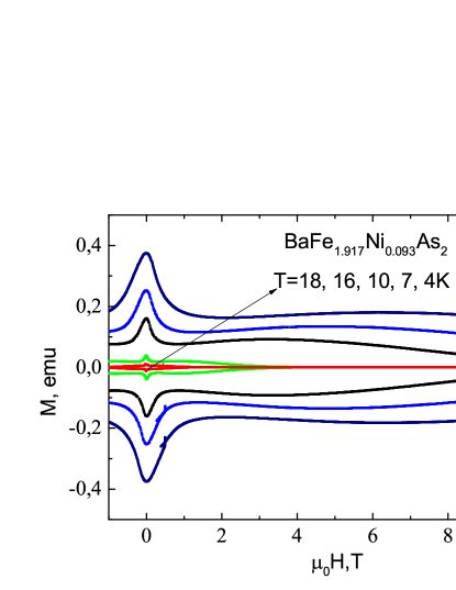
Figure 1 shows typical isothermal magnetization M(H) loops (MHL) measured at several temperatures from 4 to 18 K in magnetic fields up to 9 T for BaFe1.907Ni0.093As2 single crystal. The almost perfect symmetry of the MHLs indicates domination of the bulk pinning and exhibits no magnetic background. Therefore, we conclude our sample contains negligible amount of magnetic impurities Ba and shows bulk vortex pinning. Additionally, in MHLs of BFNA single crystal one can see the second magnetization peak (SMP) Refb or the “fish-tail”. The observed fish-tail for the present Ni-doped single crystal is similar to that seen earlier for Co, Na, and P-doped Ba-122 single crystals Refc ; Refd . This implies the SMP in the MHL is common to the Ba-122 superconductors Refe .
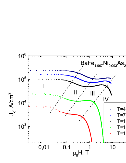
According to the Bean model for current distribution Reff , is given by the formula: , where , and are the sample transverse dimensions with . We calculate from MHLs using the Bean model with effective sample dimensions mm3. Figure 2 shows on the log-log plot the field dependence of obtained from the MHLs data.
Haberkorn et al. Refg has shown that J behaviour exhibits several regimes: (I) low-field part associated with the single vortex regime; (II) a power-law dependence , associated with strong pinning centers; (III) a regime related with the fishtail; and (IV) a fast drop in where the vortex dynamics changes to plastic. As one can clearly see several marked area in Fig.2 are related with different pinning regimes. Regime I is observed at low fields up to 150 Oe. The power law behaviour extends up to 2 T. The obtained values of were from 0.45 to 0.58 for temperature interval between 18 to 4 K respectively. The value of the exponent is in good agreement with the theoretical prediction of . Such value of the exponent indicates strong vortex pinning Refl . The III regime behaviour is related with crossover or/and correlation between strong pinning by defects and weak intrinsic pinning by large amount of centers —the so-called “caging” effect (CE). This leads to the conclusion that pinning in fields T originates from different mechanisms. The IV region is associated with disruption of magnetic vortices from pinning centers, which leads to the dissipation of energy and a rapid drop of the critical current. The onset of the IV regime is the limit of practical applicability of the superconductor. It should be noted that almost the same behavior of is observed in optimally doped BFNA.
4 Andreev spectroscopy
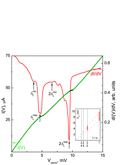
Figure 3 shows current-voltage characteristic (CVC) and its derivative for a ScS-array formed in BFNA single crystal. The bias voltage axis was scaled with the natural to a single-junction spectrum, therefore, all the data corresponds to a single junction. The pronounced foot in CVC is typical for a clean SnS-mode OTBK ; Averin ; Arnold ; Kummel . To check whether the contact is ballistic, we take the normal-state bulk resistivity cm for the sample under study, and the contact resistance (see Fig. 3) and plug them into the Sharvin formula Sharvin . Given the product of the bulk resistivity and the carrier mean free path for Ba-122 determined elsewhere Xu cm, we immediately get , thus proving the contact is ballistic and favourable for MARE observation. Note the both parts of CVC (the positive and negative current) in Fig. 3 are symmetrical and non-hysteretic. In the dI(V)/dV spectrum (red line), two Andreev subharmonics for the large gap (observable in bias voltages mV, and mV) are well pronounced. The position of these dips determine the large gap meV. Taking into account a strongly asymmetrical shape of both dips, one may suppose a gap anisotropy in the space Devereaux ; BJ . If it is the case, the aforementioned dips at , correspond to larger extremum of the gap distribution meV. The features located at 6.6 and 3.3 mV are very likely the subharmonics for the lower extremum meV. Given this assumption, the large gap anisotropy may be estimated as . The complex fine structure of the observed Andreev dips is caused by the -plane gap distribution; it seems to differ from the simple predicted e.g. in Kontani . In the inset of Fig. 3, we show the position of doublets versus their inverse number . The linear dependence crossing the origin proves these features are related to one and the same SGS. The above figures demonstrate the observation of IMARE in BFNA single crystals.
Two Andreev spectra of the SnS-arrays formed sequentially (after a mechanical readjustment) in one and the same BFNA sample are shown in Fig. 4. Despite the different contact resistance, the spectra look similarly and possess features for both the large and the small gap. The main doublet-like dip located at mV is nearly twice wider than the second feature for the large gap at mV. Together, these dips are the subharmonics for the anisotropic large gap meV, whereas their width corresponds to anisotropy of the large gap. The latter value is close to that determined using data of Fig. 3. The intensive doublets at mV do not correspond to the large gap SGS, and therefore, may be interpreted as related to the small gap with moderate anisotropy meV ( anisotropy). Note that for the two spectra shown in Fig. 4, the position of both-gap features coincide. The gap values remain still unchanged during the contact readjustment confirming both a high quality of cryogenic interfaces and a high homogeneity of the single crystal under study. The uniform distribution of dopants within the typical contact area reduces a contribution of -pinning mechanism (associated with a spatial variation of the superconducting transition temperature throughout the sample). Therefore, pinning in the studied Ba-122 samples may be caused by randomly distributed point-like pinning centers (-pinning) at a sub-nanometer scale Blatter .
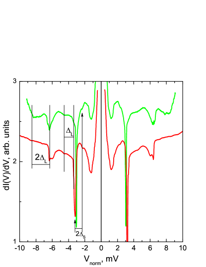
From the IMARE spectra, we determined the BCS-ratio . It is similar to that determined earlier in IMARE experiments with K-doped Ba-122 single crystals Ba ; BKFA and exceeds the standard weak-coupling limit 3.52, thus proving a strong coupling. Taking into account the moderate gap anisotropy determined here, the BCS-ratio well covers all the range of estimated in specific heat and measurements with the BFNA samples from the same batch Ba2016 , and in infrared spectroscopy and magnetization experiments with nearly optimal K-doped Ba-122 single crystals with K Ba ; BKFA . It is also consistent with other published data for Ba-122 Evtushinsky ; Hardy ; Pramanik ; Khasanov ; Yin . The BCS-ratio for the small gap is and lies well below the weak-coupling limit, thus proving the presence of the -space proximity effect and substantial interband interaction.
5 Conclusions
We have studied the field dependence of the critical-current density and the structure of superconducting order parameter in nearly optimally doped BaFe2-xNixAs2 () single crystals. Our results indicate the strong bulk pinning in BFNA by random nanoparticles dominates at low fields. At higher fields, the strong pinning may originate from a combination of several mechanisms related to point defects. Using intrinsic multiple Andreev reflections effect (IMARE) observed in BFNA, we directly determine the values of two distinct superconducting gaps with a moderate anisotropy in a -space: meV (the range corresponds to anisotropy), meV ( anisotropy). The BCS-ratio for the large gap is close to that for K-doped Ba-122 Ba and evidences for a strong coupling in the -bands.
Acknowledgements.
We thank M. Abdel-Hafiez, Y. Chen, H. Kontani, Yu.F. Eltsev for useful discussions and the samples presented. The work was partially supported by the Council of the President of the Russian Federation for Support of Young Scientists (project no. MK-5699.2016.2). VMP acknowledges support from RSCF (no. 16-42-01100). The measurements were partly done using research equipment of the Shared Facilities Center at LPI.References
- (1) Y. Kamihara, T. Watanabe, M. Hirano, and H. Hosono, J. Am. Chem. Soc. 130, 3296 (2008).
- (2) M. Rotter, M. Tegel, D. Johrendt, I. Schellenberg, W. Hermes, and R. Pöttgen, Phys. Rev. B 78, 020503(2008).
- (3) A.S. Sefat, R. Jin, M.A. McGuire, B.C. Sales, D.J. Singh, and D. Mandrus, Phys. Rev. Lett. 101, 117004 (2008).
- (4) B. Kalisky, J.R. Kirtley, J.G. Analytis, J.-H. Chu, I.R. Fisher, and K.A. Moler, Phys. Rev. B 83, 064511 (2011).
- (5) S. Demirdis, C.J. van der Beek, Y. Fasano, N.R. Cejas Bolecek, H. Pastoriza, D. Colson, and F. Rullier-Albenque, Phys. Rev B 84, 094517 (2011).
- (6) N. Haberkorn, B. Maiorov, I.O. Usov, M. Weigand, W. Hirata, S. Miyasaka, S. Tajima, N. Chikumoto, K. Tanabe, and L. Civale, Phys. Rev. B 85, 014522 (2012)
- (7) D.V. Evtushinsky, D.S. Inosov, V.B. Zabolotnyy, A. Koitzsch, M. Knupfer, B. Büchner, M.S. Viazovska, G.L. Sun, V. Hinkov, A.V. Boris, C.T. Lin, B. Keimer, A. Varykhalov, A.A. Kordyuk, and S.V. Borisenko, Phys. Rev. B 79, 054517 (2009).
- (8) P. Seidel, Supercond. Sci. Technol. 24, 043001 (2011).
- (9) S. Maiti, A.V. Chubukov, Phys. Rev. B 87, 144511 (2013).
- (10) T. Saito, S. Onari, and H. Kontani, Phys. Rev. B 88, 045115 (2013).
- (11) Ya.G. Ponomarev, K.K. Uk, M, Lorenz. Inst. Phys. Conf. Ser. 167, 241 (2000).
- (12) Ya.G. Ponomarev, S.A. Kuzmichev, T.E. Kuzmicheva, M.G. Mikheev, M.V. Sudakova, S.N. Tchesnokov, O.S. Volkova, A.N. Vasiliev, V.M. Pudalov, A.V. Sadakov, A.S. Usol’tsev, Th. Wolf, E.P. Khlybov, J. Supercond. Novel Magn. 26, 2867 (2013).
- (13) Ya.G. Ponomarev, S.A. Kuzmichev, M.G. Mikheev, M.V. Sudakova, S.N. Tchesnokov, N.Z. Timegaleev, A.V. Yarigin, E.G. Maksimov, S.I. Krasnosvobodtsev, A.V. Varlashkin, M.A. Hein, G. Miller, H. Piel, L.G. Sevastyanova, O.V. Kravchenko, K.P. Burdina, B.M. Bulychev, Solid State Comm. 129, 85 (2004).
- (14) Ya.G. Ponomarev, S.A. Kuzmichev, N.M. Kadomtseva, M.G. Mikheev, M.V. Sudakova, S.N. Chesnokov, E.G. Maksimov, S.I. Krasnosvobodtsev, L.G. Sevast yanova, K.P. Burdina, B.M. Bulychev, JETP Lett. 79, 484 (2004).
- (15) T.E. Kuzmicheva, S.A. Kuzmichev, M.G. Mikheev, Ya.G. Ponomarev, S.N. Tchesnokov, Yu.F. Eltsev, V.M. Pudalov, K.S. Pervakov, A.V. Sadakov, A.S. Usoltsev, E.P. Khlybov, L.F. Kulikova, EPL 102, 67006 (2013).
- (16) M. Octavio, M. Tinkham, G.E. Blonder, and T.M. Klapwijk, Phys. Rev. B 27, 6739 (1983).
- (17) D. Averin and A. Bardas, Phys. Rev. Lett. 75, 1831 (1995).
- (18) G.B. Arnold, J. Low Temp. Phys. 68, 1 (1987).
- (19) R. Kümmel, U. Gunsenheimer, and R. Nicolsky, Phys. Rev. B 42, 3992 (1990).
- (20) T.P. Devereaux and P. Fulde, Phys. Rev. B 47, 14638 (1993).
- (21) S.A. Kuzmichev, T.E. Kuzmicheva, A.I. Boltalin, and I.V. Morozov, JETP Lett. 98, 722 (2013).
- (22) S.A. Kuzmichev, T.E. Kuzmicheva [in press].
- (23) J. Moreland, J.W. Ekin, J. Appl. Phys. 58, 3888 (1985).
- (24) A.F. Andreev, Sov. Phys. JETP 19, 1228 (1964).
- (25) H. Nakamura, M. Machida, T. Koyama, and N. Hamada, J. Phys. Soc. Jpn. 78, 123712 (2009).
- (26) Ya.G. Ponomarev, B.A. Aminov, M.A. Hein, H. Heinrichs, V.Z. Kresin, G. Müller, H. Piel, K. Rosner, S.V. Tchesnokov, E.B. Tsokur, D. Wehler, K. Winzer, A.V. Yarygin, K.T. Yusupov, Physica C 243, 167 (1995).
- (27) Ya.G. Ponomarev, S.A. Kuzmichev, M.G. Mikheev, M.V. Sudakova, S.N. Tchesnokov, O.S. Volkova, A.N. Vasiliev, T. Hänke, C. Hess, G. Behr, R. Klingeler, and B. Büchner, Phys. Rev. B. 79, 224517 (2009).
- (28) M. Abdel-Hafiez, P.J. Pereira, S.A. Kuzmichev, T.E. Kuzmicheva, V.M. Pudalov, L. Harnagea, A.A. Kordyuk, A.V. Silhanek, V.V. Moshchalkov, B. Shen, H.-H. Wen, A.N. Vasiliev, and X.-J. Chen, Phys. Rev. B, 90, 054524 (2014).
- (29) S. Salem-Sugui, L. Ghivelder, A.D. Alvarenga, L.F. Cohen, H. Luo, and X. Lu, Phys. Rev. B, 84, 052510 (2011).
- (30) A. Yamamoto, J. Jaroszynski, C. Tarantini, L. Balicas, J. Jiang, A. Gurevich, D.C. Larbalestier, R. Jin, A.S. Sefat, M.A. McGuire, B.C. Sales, D.K. Christen and D. Mandrus, Appl. Phys. Lett. 94, 062511 (2009).
- (31) A.K. Pramanik, S. Aswartham, A.U.B. Wolter, S. Wurmehl, V. Kataev, B. Büchner, J. Phys.: Condens. Matter 25, 495701 (2013).
- (32) D. Song, S. Ishida, A. Iyo, M. Nakajima, J.-I. Shimoyama, M. Eisterer, H. Eisaki, Sci. Rep. 6, 26671 (2016).
- (33) C.P. Bean, Rev. Mod. Phys. 36, 31 (1964).
- (34) N. Haberkorn, B. Maiorov, M. Jaime, I. Usov, M. Miura, G.F. Chen, W. Yu, and L. Civale, Phys. Rev. B 84, 064533 (2011).
- (35) C. J. van der Beek, G. Rizza, M. Konczykowski, P. Fertey, I. Monnet, T. Klein, R. Okazaki, M. Ishikado, H. Kito, A. Iyo, H. Eisaki, S. Shamoto, M.E. Tillman, S.L. Bud ko, P.C. Canfield, T. Shibauchi, and Y. Matsuda, Phys. Rev. B 81, 174517 (2010).
- (36) Yu.V. Sharvin, Sov. Phys. JETP 21, 655 (1965).
- (37) Z. Xu, Q. Tao, L. Li, J. Shen, X. Lin, G. Cao, Physica C 470, S447 (2010).
- (38) G. Blatter, M.V. Feigel’man, V.B. Geshkenbein, A.I. Larkin, and V.M. Vinokur, Rev. Mod. Phys. 66, 1125 (1994).
- (39) A.V. Muratov, Yu.A. Aleshenko, A.A. Kordyuk, T.E. Kuzmicheva, S.A. Kuzmichev, V.M. Pudalov, A.V. Sadakov, S.Yu. Gavrilkin, M. Abdel-Hafiez, and A. Bianconi [in press].
- (40) M. Abdel-Hafiez, H. Xiao, S.A. Kuzmichev, T.E. Kuzmicheva, A.V. Sadakov, Z. He, Z. Zhu, X. Lu, H. Luo, V.M. Pudalov, P. Dai, and X.-J. Chen [in press].
- (41) F. Hardy, T. Wolf, R.A. Fisher, R. Eder, P. Schweiss, P. Adelmann, H. v. Löhneysen, and C. Meingast, Phys. Rev. B 81, 060501(R) (2010).
- (42) A.K. Pramanik, M. Abdel-Hafiez, S. Aswartham, A.U.B. Wolter, S. Wurmehl, V. Kataev, and B. Büchner, Phys. Rev. B 84, 064525 (2011).
- (43) R. Khasanov, D.V. Evtushinsky, A. Amato, H.-H. Klauss, H. Luetkens, Ch. Niedermayer, B. Büchner, G.L. Sun, C.T. Lin, J.T. Park, D.S. Inosov, and V. Hinkov, Phys. Rev. Lett. 102, 187005 (2009).
- (44) Y. Yin, M. Zech, T.L. Williams, X.F. Wang, G. Wu, X.H. Chen, and J.E. Hoffman, Phys. Rev. Lett. 102, 097002 (2009).
- (45) T.E. Kuzmicheva et al., JETP Lett. 99, 136 (2014).
- (46) T.E. Kuzmicheva et al., Physics-Uspekhi 57, 13 (2014).
- (47) Ya.G. Ponomarev et al., J. Supercond. Nov. Magn, 26, 2867 (2013).