Emergence of the stripe-domain phase in patterned Permalloy films
Abstract
The occurrence of stripe domains in ferromagnetic Permalloy (Py=Fe20Ni80) is a well known phenomenon which has been extensively observed and characterized. This peculiar magnetic configuration appears only in films with a thickness above a critical value (), which is strongly determined by the sputtering conditions (i.e. deposition rate, temperature, magnetic field). So far, has usually been presented as the boundary between the homogeneous (H) and stripe-domains (SD) regime, respectively below and above . In this work we study the transition from the H to the SD regime in thin films and microstructured bridges of Py with different thicknesses. We find there is an intermediate regime, over a quite significant thickness range below dcr, which is signaled in confined structures by a quickly changing domain-wall configuration and by a broadening of the magnetoresistance dip at the coercive field. We call this the emerging stripe-domains (ESD) regime. The transition from the ESD to the SD regime is accompanied by a sharp increase of the magnetoresistance ratio at the thickness where stripes appear in MFM.
I Introduction
Alloys of iron and nickel, known as permalloys, are much exploited in applications because of their particular magnetic properties. In particular, Permalloy with approximately 20% Fe and 80% Ni (Py=Fe20Ni80) is widely used in magnetoelectronic devices such as, for example, magnetic recording media, magnetic transducers, MRAM and magnetic cores of inductors amos ; khizroev ; dastagir ; zhao . At this specific composition the values of magnetostriction and magnetocrystalline anisotropy are nearly zero. As a result, Py is characterized by a very high permeability () and low coercive field (below 1 mT), which makes it a “soft” ferromagnet.
In Py thin films, because of the demagnetizing field, the magnetization normally lies in-plane. However, if grown under particular conditions, Py films can have a certain amount of Perpendicular Magnetic Anisotropy (PMA). This leads to the occurrence of magnetic stripe domains (SDs) saito ; magn_domains . If the PMA is small, as in the case of Py, the domain state is called “weak stripes”: the main magnetization component is still in the film plane but it is tilted alternatively upwards and downwards by a small out-of-plane componentmagn_domains , as sketched in Fig. 1.
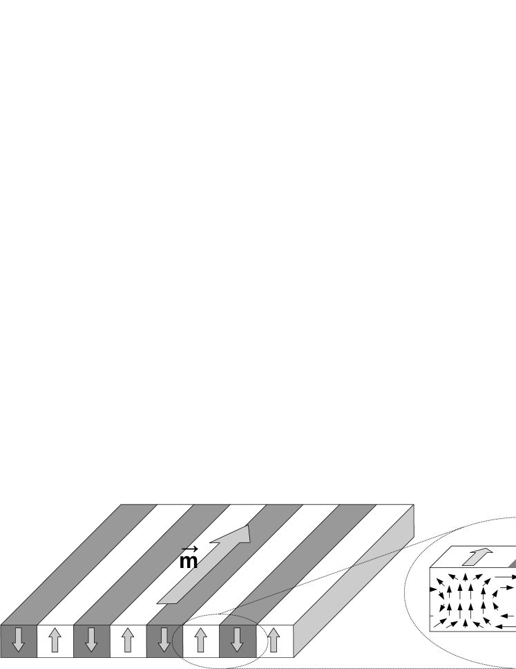
SDs appear only above a certain value of the film thickness, given by , where is the exchange stiffness constant and is the perpendicular anisotropy constant. SDs in Py have been experimentally well characterized and their peculiar properties have been exploited in magnetic devices for several purposesdastagir ; belkin ; vlasko . However, to our knowledge, little work has been done to describe the transition regime below . Micromagnetic simulations were performed to investigate the type of domain walls occurring in narrow strips (Ref. magn_domains , Ch.3.6) as function of thickness and perpendicular anisotropy, but those results do not signal the changes we observe with increasing thickness.
As a matter of fact, values for are hardly ever determined, nor quantitatively compared to values extracted for from e.g. magnetization measurements. Instead, studies on stripe domains are simply performed on films with thicknesses well above an inferred critical thickness. Our interest in the magnetic structure of Py films derives from studies of superconducting Py/Nb multilayers, in which unusual behavior was found of the superconducting critical fields. For relatively large thicknesses (of the order of 200 nm) but below the onset of stripe domains we find indications for a long range proximity effect and the occurrence of odd-frequency triplet Cooper pairs, which appears to be the consequence of an inhomogeneous magnetic state in the ferromagnetic layerberg_2001 ; esch_phystod . A discussion of the proximity effects will be given elsewhere, but it also led us to a systematic study of the magnetic behavior of our Py films as function of thickness, using Magnetic Force Microscopy (MFM), ferromagnetic resonance (FMR), SQUID magnetometry and magnetoresistance measurements (MR). We study the behavior of full films as well as of confined structures, such as bars and squares, and we also use micromagnetic simulations to compare with experimental results. For confined geometries, the results show that the influence of the perpendicular anisotropy can be found well below the stripe domain (SD) regime, in particular in the structure of domains and domain walls, and the behavior of the MR. This leads us to identify two different regimes below the SD regime: a fully homogeneous (H) regime for thin samples, and a regime which we call emerging stripe-domains (ESD), for intermediate thicknesses. In the ESD regime the perpendicular anisotropy clearly influences the magnetic configuration even if without forming full stripes. In the description we use an operational definition of as the thickness where stripes appear in MFM measurements, which in our case is around 300 nm. We show that this coincides with a strong increase in the magnitude of the magnetoresistance dip around the coercive field. On the other hand, the MR data display a decided broadening of the dip in the regime between 150 nm and 300 nm (ESD). Thus, we argue that the homogeneous magnetic state already disappears at less than 0.5 . We also discuss how this picture is to be reconciled with out in-plane and out-of-plane magnetization data.
The paper is organized as follows: in Sec.II, we describe sample preparation details, measurement and simulation methods; in Sec.III.1 we describe MFM images of Py films and structures in the three different thickness regimes, in Sec.III.2, we present FMR and magnetization vs field measurements of Py films, used to determine the critical thickness, while in Sec.III.3 we show and discuss the magnetoresistance measurements; micromagnetic simulations of confined structures are presented in Sec.IV and, to conclude, Sec.V highlights the main results of our study.
II Experimental details and methods
Py films were deposited on Si(100) substrates in a ultrahigh vacuum DC diode magnetron sputtering system, at room temperature. The base pressure reached was approximately 2.7 mbar, while the deposition was done in an Ar pressure of 2.7 mbar. The typical deposition rate, measured by a calibrated crystal monitor, was 0.30 nm/s. Several series of Py films with different thickness were prepared, called S1 (50, 200 and 350 nm), S1b (290 nm), S2 (50, 100, 150, 200, 250, and 360 nm), S3 (100, 125, 150, 175, 200, 225, 250, 275, 300, 325 and 350 nm) and S3b (380 nm). The growth conditions were nominally the same for all samples, but they were grown at different times. The samples of the same series were grown in succession, within one or two days. Magnetic imaging was both performed on as-grown films and on films patterned into small structures via e-beam lithography followed by Ar-ion etching. The structures were small squares, as well as bridges with contacts in standard 4-probe geometry (current contacts outside, voltage contacts inside) for the transport measurements. For all devices on which transport measurements were made, the width of the bridge was 10 m and the distance between the voltage contacts 100 m.
Magnetic imaging was performed on both unpatterned (S1 series) and patterned samples (125 nm and 225 from the S3 series, 380 nm from the S3b series) with standard Magnetic Force Microscopy (MFM), in lift height mode. Magnetic hysteresis loops of unpatterned samples from the S2 series were taken with a commercial (Quantum Design) SQUID magnetometer, while the broadband microstrip FMRdenysenkov was performed on the unpatterned samples of the S2 series. An Agilent E8361A PNA Millimeter Wave Vector Network Analyzer (10MHz-67GHz) was used to apply a microwave signal to the samples and to measure the magnetic absorption. The signal is injected into a microstrip line on top of which the sample is located. We register the complex microwave scattering parameter S21 as a measure of the microwave magnetic absorption. The FMR responses for all samples were measured at room temperature by sweeping the frequency for fixed external applied field in the 0.25-15 GHz range. This process was repeated for several applied field values ranging form -50 mT to 50 mT.
The electrical measurements were done with an automated measurement platform (PPMS), with the magnetic field applied in-plane and along the current direction, on the samples of the S3 series (except for the 225 nm thickness). We need to point out that the magnetoresistance curves presented (Fig.6) are affected by a systematic offset along the -axis (up to 20 mT), which is positive for backward sweeps and negative for forward sweeps, and dependent on the starting field value. Because of that, the dip in the MR curve occurs before the field reaches zero value. This error, introduced by the magnet remanence (of PPMS) at low fields, is more extensively discussed in the Supplementary Information. The offset becomes a problem when determining the exact coercive field; however it does not influence the discussion below, for which only the MR ratio and the dip width are relevant.
Micromagnetic simulations were performed with the software package oommfoommf (object oriented micromagnetic framework) for square structures m2 and thickness in the different regimes (100, 225, 285 and 345 nm). The cell size used for the calculations is nm3 or smaller and the damping coefficient is 0.5. The details for the magnetic parameters used are presented in Sec.IV.
III Experimental results and Discussion
III.1 Magnetic Force Microscopy
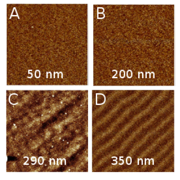
MFM images of unpatterned Py films with thicknesses in the three different regimes from the S1 series (50 nm, 200 nm and 350 nm) and S1b (290 nm) are shown in Fig.2. For the thickest sample, clear stripe domains are observed (Fig.2-D). Darker and brighter regions (domains) represent areas where an out-of-plane component of the magnetization is detected and points upwards or downwards, respectively. The domain width is approximately 330 nm, which is of the same order of the thickness of the sample, as predicted for weak stripe domainsmagn_domains . No contrast is observed for the samples 50 nm (Fig.2-A) and 200 nm thick (Fig.2-B), which suggests that either the magnetization is fully in-plane or the out-of-plane component is below the sensitivity of our MFM detection. For the 290 nm thick sample (Fig.2-C) we can observe non-homogeneous magnetic areas, even if they are not fully developed in stripes yet. Given these observations, the critical thickness for our samples can be defined to be slightly above 300 nm.
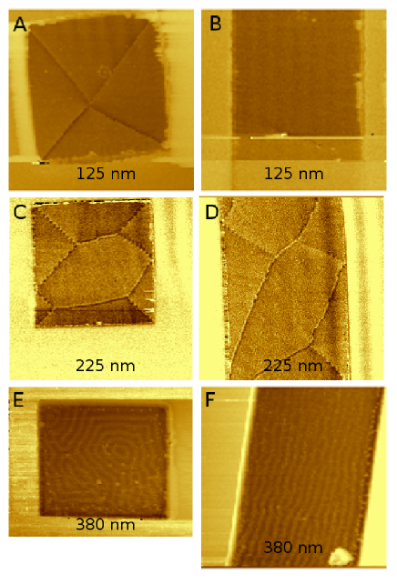
To further investigate the magnetic configuration at different thicknesses, MFM measurements were performed also on patterned films of the S3 and S3b series, in particular on squares of approximately m2 (see Fig.3-A,C,E) and long bars of 10 m wide (see Fig.3-B,D,F), in the three different regimes. Fig.3-E and -F show that for samples 380 nm thick (S3b series), well above , the confinement does not hinder the presence of stripe domains. In Fig.3-E the effects of the demagnetizing fields lead to rotations of the stripe directions, producing maze-like domain configurations. Also in Fig.3-F the stripes are clearly visible and they are aligned along the bar, parallel to the magnetic field previously applied to magnetize the virgin sample. In this case the stripes turn out to be stronger in the proximity of the extremity of the bar (the edge is just outside the scan range) and they become weaker while moving far away from it. The reason is that at the center of the bar the shape anisotropy forces the magnetization to be more in-plane, weakening the out-of-plane component. At the extremity, instead, the influence of the shape anisotropy is weaker and the stripes are less affected. Fig.3-A shows a structure of 125 nm thickness. Here, as we expect, the magnetization is fully in-plane, so the magnetic configuration is mainly determined by the demagnetizing energy, which results in four triangular closure domains, with Bloch domain walls. For the 225 nm thick sample shown in Fig.3-C we observe a magnetic configuration which is in between the other two regimes: there are triangular closure domains and a large center domain where the magnetization is fully in-plane and no stripes are visible; most of the domain walls now seem to be “broken”, with alternating up-down components, indicating that the out-of-plane anisotropy is playing a role, even if it is not strong enough to generate stripes. Such a difference is clearly visible also for the bars, as can be observed by comparing Fig.3-B (125 nm thick) and Fig.3-D (225 nm). In the first case triangular domains, similar to the ones observed in Fig.3-A, are confined to the extremities (not shown in the image), but the magnetization is homogeneously in-plane in the rest of the structure. In the second case (Fig.3-D), the domains are present in the whole bar with the characteristic configuration observed also in Fig.3-C.
III.2 FMR and Magnetometry
As discussed in the Introduction, the critical thickness can be, in principle, determined by estimating the uniaxial (weak) out-of-plane anisotropy and the exchange constant .
To determine the exchange constant of Py independently from the magnetization measurements, we performed FMR experiments on the films from the S2 series. Fig.4 shows the dependence of the energy absorption as function of magnetic field and frequency for the 200 nm thick sample as a color map.
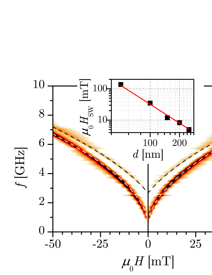
The spectrum shows the main FMR mode corresponding to the homogeneous excitation of the film that fits well the expected field dependence given by the Kittelkittel equation (white dashed line)
| (1) |
being the gyromagnetic ratio. The results for the main mode are very similar in all samples. The value of mT extracted from these fittings agrees nicely with the one obtained from SQUID magnetometry.
Next to the main absorption line, a second resonance (fitted by the black dashed line in Fig.4) appears in the spectrum corresponding to the first discrete spin wave (SW) mode associated with the thickness of the sample, . In this case the frequency dependence follows the expression
| (2) |
where is the spin wave field which for the first mode is . The distance in frequency between the main mode and the first SW mode obviously depends on the sample thickness. We can use this dependence to obtain the exchange stiffness constant, , in our samples. The inset of Fig.4 shows as a function of the sample thickness, , together with the fit to the dependence. From this fitting we extract a value of J/m, which agrees with the usual values for Py.
The value of can be estimated using the following relations, which are valid in the case of weak out-of-plane anisotropymurayama :
| (3) | |||
| (4) |
where , are the fields at which saturation is reached when the field is applied respectively parallel or perpendicular to the film plane, and is the saturation magnetization. By determining and from the magnetization loops, and can be estimated. In Fig.5 we show magnetic hysteresis loops for unpatterned films of different thicknesses, with the field applied parallel to the film plane.
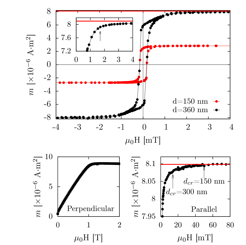
The top graph shows the measurements for 150 nm (red squares) and 360 nm (black circles) thick samples from the S2 series. The 360 nm thick sample shows roughly linear decrease of the magnetization between the saturation field and the remanent field, which is a typical signature of the presence of stripe domains. From this curve, is estimated to be about 2 mT. , determined from the bottom left panel which shows a zoom of the loop of the same sample but with the field applied perpendicular to the film plane, is about 1000 200 mT. These values lead to an anisotropy J/m3, which, combined with the value of , gives 800 nm, well above the experimental observation. However, by looking more closely to the magnetization curve when the field is in-plane (a zoom is showed in the bottom right panel), we can notice that at 2 mT the magnetization is not fully saturated: the value keep on increasing with a much lower slope and the saturation of 8.110-6 Am2 is reached at around 50 mT. The variation of the magnetization value between 2 mT and 50 mT is very small and could be due either to the effect of the out-of-plane anisotropy or to trapped magnetic moments getting aligned or both. 50 mT sets the maximum for the possible values of (minimum ). With this value, the critical thickness results to be about 150 nm ( J/m3), which is lower than what obtained from MFM measurements. A of 300 nm, can be obtained if 14 mT ( J/m3), that is compatible with the magnetization data. Interestingly, the curves for the samples 200 and 250 nm thick of the S2 series (not shown here) also show a linear decrease down to remanence, even if less pronounced. As mentioned above this behavior is a signature of stripe-like magnetic domains, but for this range of thicknesses no clear stripes are observed with MFM.
The value of was estimated for this particular set of samples of the S2 series. However, a change in the
deposition conditions can influence the magnetic properties of Py (especially ), which results in a different
value for . In general, negligible differences are expected amongst samples prepared in the same deposition
system. However, changes to the setup which influence the deposition rate or the magnetic configuration inside the
chamber can lead to a variation of .Therefore is not to be taken as an exact value, but as an
approximate value of the thickness where to expect
the appearance of stripes. For our discussion we will consider a value of about 300 nm
Another point to note is that the numbers confirm that we are dealing with the weak stripe regime. Defining the quality
factor Q = 2/(), we find Q 0.05. Note that is sometimes called
, the stray field energy coefficient. Strong stripes, where the magnetization direction remains perpendicular to
the surface for all values of the film thickness occur for Q
> 1 magn_domains ; virot12 , and our films are clearly far from that regime.
III.3 Magnetoresistance measurements
Magnetometry and MFM measurements suggest the presence of a non homogeneous magnetization in a large thickness regime below the appearance of stripes. For the samples in this regime, the magnetic curves show a linear behavior and MFM images for patterned samples do indicate the presence of an out-of-plane magnetic component, resulting in cross-tie-like domain walls.
To gain more insight we performed magnetoresistance (MR) measurements on 10 m wide bridges. As shown in Sec.III.2, the confinement does not affect the presence of stripes. Moreover, characterization of the relation between resistance and magnetic configuration in patterned samples can become useful when Py has to be combined with other layers in devices such as S/F/S junctions. For this reason all measurements were taken at low temperature (5 K).
.
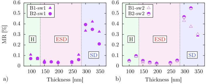
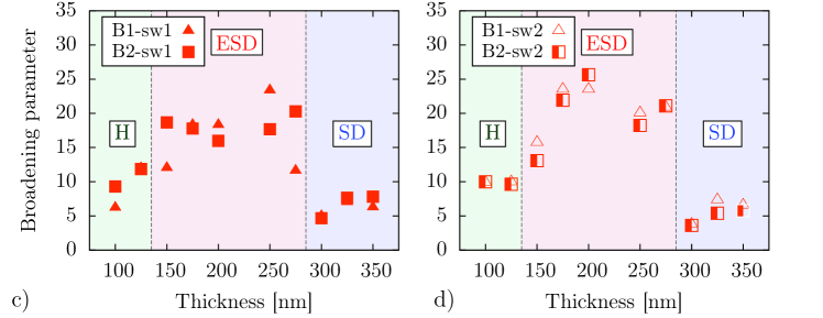
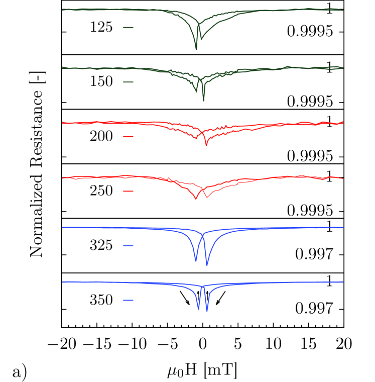
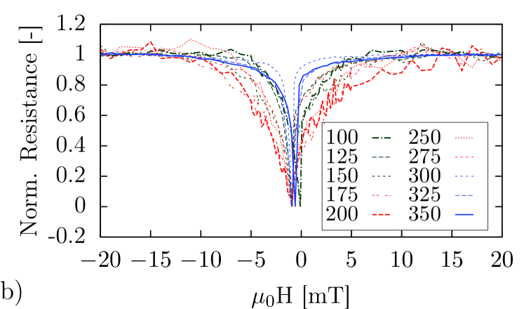
In Fig.6(a) we show two curves for each of the three thickness regimes, normalized by the resistance value at -20 mT (). The field is here applied in-plane and parallel to the current direction (longitudinal configuration). In order to make sure that the SDs were formed, we applied a high field (typically 1.5 T) along the bridge before starting each magnetic sweep. The same procedure was followed for all samples, also for the thicknesses where we did not expect stripes. As expected, the curves show a positive anisotropic magnetoresistance and hysteretic behavior with a switch of the resistance corresponding to the coercive field. It is important to note the different scale of the y-axis for the thicker samples (325, 350 nm): for these samples the magnetoresistance ratio is one order of magnitude higher than for the samples in the other two regimes. This large increase of MR ratio while passing from the ESD to the SD regime, is highlighted in Fig.7(a,b), where the value of the MR ratio is plotted versus Py thickness for all the samples of the series. We defined the MR ratio as , with the resistance value of the minimum of the curve. Left and right panels show the values obtained from the backward and forward sweep, respectively. Two bridges (denoted B1 and B2) were patterned on each film and the values for both structures of the same sample are shown together in each panel. The plots show a sharp transition in MR ratio between 275 nm and 300 nm.
Another interesting feature observed in the curves of Fig.6(a) is the width of the MR dip, which is larger for the curve in the intermediate regime. The difference is more visible in Fig.6(b), where all the curves of the measured series are plotted, normalized by and the dip height. In this way all the dips have the same height and their shape can be directly compared. From this graph is evident that the curves of the intermediate thickness regime are broader compared to thicker and thinner samples. To quantify this change in shape of the MR curves we define a broadening parameter, , given by the area enclosed by the normalized curves of Fig.6(b). The results are summarized in Fig.7(c,d), where the values of are presented for the same structures and sweeps of Fig.7(a,b). The graphs show that there is a clear broadening of the MR curve (higher value of ) in the intermediate regime. The broadening sets in at a thickness of about 150 nm, which interestingly enough is the value of the estimated , and decreases in between 275 nm and 300 nm, in conjunction with the strong increase of the MR ratio.
The combination of Fig.7(a,b) and (c,d) makes us identify three different magnetic regimes (in the plots separated by dashed vertical lines and different background colors): the first for thicknesses below approximately 150 nm, the second between 150 nm and 280 nm and the third one above 280 nm, respectively called homogeneous (H), emerging stripe-domains (ESD) and stripe-domains (SD) regime. For the H regime, as expected, the weak out-of-plane anisotropy does not play a role and the magnetization is homogeneously in-plane. At around 150 nm we have a change in the magnetic configuration signaled by a broadening of the MR curve and the appearance of a linear behavior in the loops, even if well defined stripes are not developed yet. A second abrupt transition is observed between ESD and SD regime: the MR ratio increases by one order of magnitude, at the same time the broadening returns to a low value. Above this threshold the standard SDs, as known from the literature, are also observed in the magnetic measurements. The existence of an intermediate non-homogeneous state could also explain the data of Ref.ramos, , where the FMR spectra for the intermediate thickness (sample S1) shows a peculiar double peak feature, while MFM and do not show any signature of inhomogeneity. At this moment we can only speculate on the precise nature of the ESD regime. It is clearly characterized by the absence of long range order in the perpendicular component of the magnetization. Looking back at Fig.1, this could be either considered as an extended domain wall, or as a state in which the perpendicular components of the magnetization are not ordered yet. Local probes of the magnetization, such as with polarized neutrons, may shed more light on the nature of the ESD.
IV Micromagnetic simulations
The results of Sec.III.1 and III.3 suggest that in the ESD regime the magnetization is not as homogeneous as one would expect. In order to better characterize this intermediate regime, we performed micromagnetic calculations by using the oommf software package oommf . We simulated confined structures, in particular squares m2, with thicknesses in the three regimes: 100, 225, 285 and 345 nm. The parameters used for exchange stiffness and saturation magnetization are the ones obtained from FMR experiments (see Sec.III.2), namely J/m and A/m ( mT). For the uniaxial (out-of plane) anisotropy we chose J/m3, the value extrapolated from MFM measurements (Sec.III.2). In Fig.8 we present the results, which show the magnetization in the middle plane of the sample, that is the -plane at half of the thickness.
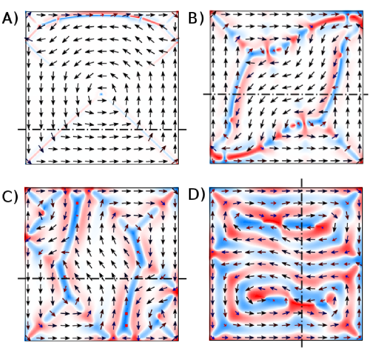
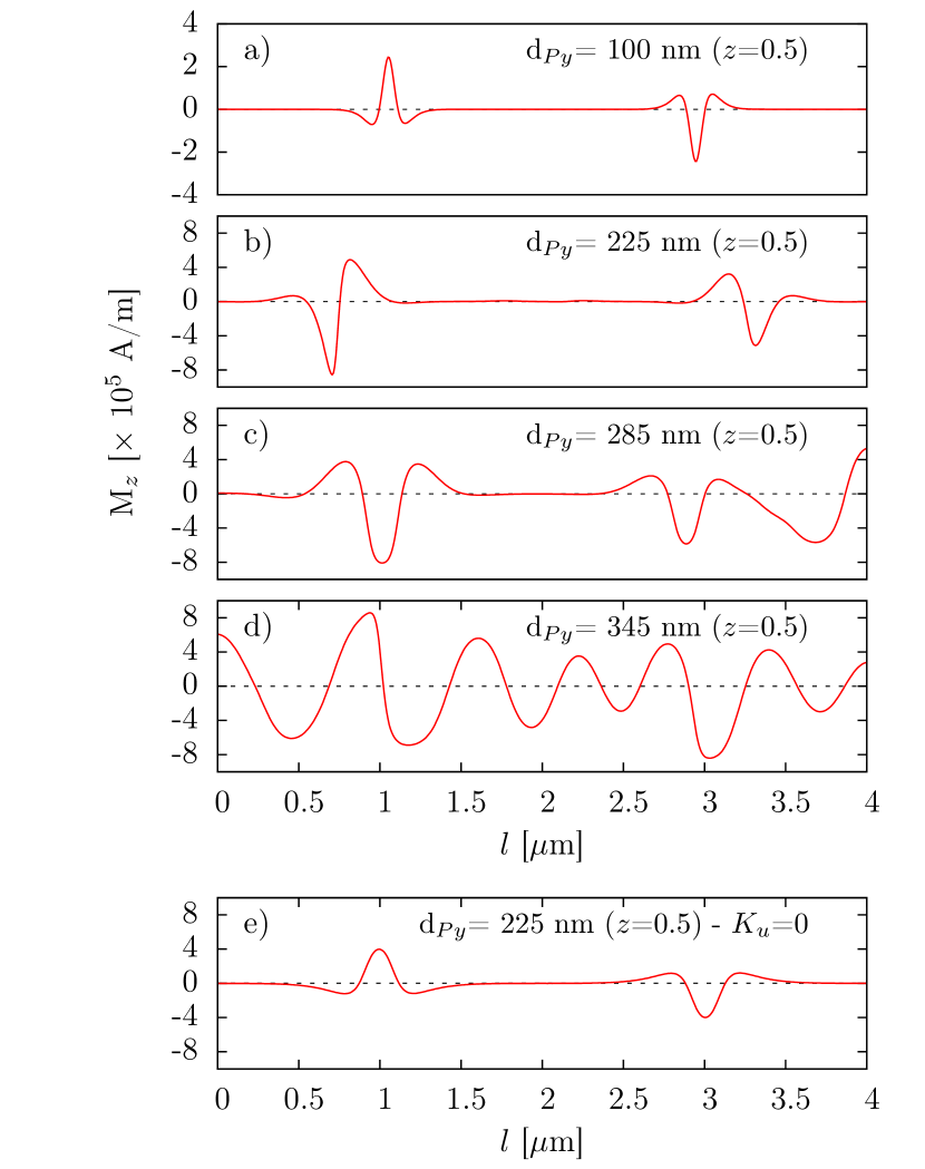
The out-of-plane component of the magnetization is represented by the color scale from red (>0) to blue (<0), while the arrows show the direction of the in-plane magnetization. For ease of comparison, Fig.9a, b, c and d show the behavior of the out-of-plane magnetization when taking a cross-section along a line of the square structures, as shown in Fig.8 (dot-dash lines). The simulations quite accurately reproduce the magnetic configurations observed with MFM on m2 squares as presented in Fig.3. For the thinnest structure in Fig.8A (100 nm, to be compared with Fig.3A) four closure domains are visible, divided by the diagonals of the square, where an out-of-plane component of the magnetization is barely visible although it shows up in the cross-section in Fig. 9a. Stripe domains appear in the structure 350 nm thick (Fig.8D, cf. Fig.3E). The stripe width is of the order of 300 nm, in agreement with the experimental value. Interestingly, the simulation qualitatively reproduce the domain structure found in the ESD regime: in Fig.8B the closure domains are smaller than in Fig.8A, and two types of walls appear, both of which are also visible in Fig.3C : “broken” domain walls which show a sequence of red-blue equal to up-down magnetization directions; and walls which consist of an up and a down component running parallel to each other and separate closure domains with anti-parallel in-plane magnetization. Such walls, with an up and a down component, are known as asymmetric Bloch walls. The rotation of the magnetization within these domain walls, also observed in MFM, is very similar to what happens in a wall between two stripe domains, with the difference that in the stripes the in-plane magnetization is parallel. As a comparison, in Fig.9e we show the cross section for a 225 nm thick structure, with no perpendicular anisotropy. In this case the simulation was run with a randomized in-plane anisotropy (with = 100 J/m3) and the cross-section is at same position as in Fig.8A. By comparing it with Fig.9b we can notice that, without perpendicular anisotropy, the domain wall configuration is the same as in the homogeneous regime (cf. Fig.9a) and the amplitude of the out-of-plane component is significantly lower than in Fig.9b. From Fig.8C we can see that, by increasing the thickness further to 285 nm, the domain walls are stretched but, because we are still below , stripe domains are not formed yet.
V Discussion and conclusions
Summarizing, we studied patterned and unpatterned films of Py with different thicknesses, below and above the critical
value for the appearance of stripe domains. Magnetoresistance measurements, combined with MFM and SQUID
magnetometry suggest the existence of three magnetic regimes: homogeneous (H), emerging stripe domains (ESD) and stripe
domains (SD). More quantitatively, their appearance can be characterized by the dimensionless parameter =
, which allows a comparison with earlier work. With the numbers given before, we have (100
nm) = 10, (225 nm) = 22.5, and with = ( it follows that
= = 28. In the H regime, up to =10, there is no evidence of stripes in
films or strips, the magnetization is fully in-plane, and in confined structures domain walls are of the simple Bloch
type. In the SD regime, above , the stripes are well developed (as it clearly appears from MFM measurements)
and they are signaled by the peculiar shape of the loops as well as from an increase of the MR ratio. In the ESD
regime between =10 and = 28 (from about 0.5 to ), stripes are not visible in
MFM images but both strips and square structures easily becomes less homogeneous. This is signaled by the peculiar
domain walls observed with MFM, which have a stronger out-of-plane component, by a linear behavior in loops and
by a broader dip characterizing the MR curves. In this regime the MR ratio is still much smaller than in the SD regime.
Micromagnetic simulations for the squares reproduce the configuration of magnetic domains and domain walls in all three
regimes quite well. In particular they show how in the ESD regime the perpendicular anisotropy leads to a richer domain
wall configuration, especially in confined structures where the influence of demagnetizing field is weaker than in
films. This might not have been expected from the phase diagram for domain wall types given in Refs.magn_domains
andramstock96 , obtained from a two-dimensional calculation for a strip of fixed width/thickness ratio 4 : 1. In
that case, asymmetric Bloch walls were found for > 7, in other words no changes occurred for the behavior
up to . For our strips, the width/thickness ratio is significantly larger, which may explain the
difference.
Concluding, we have shown how in particular the magnetoresistance evolves of Py films below the onset of the magnetic
stripe phase. A strong change in MR is found at the critical thickness, while well below the MR dips show
significant broadening. Micromagnetic simulations show good agreement with MFM measurements on confined structures, and
emphasize the difference between such structures and long strips.
VI Acknowledgments
Technical support from D. Boltje and M.B.S. Hesselberth and help from Annette Mense in the early stage of the project are gratefully acknowledged. This work is part of the research programme of the Foundation for Fundamental Research on Matter (FOM), which is part of the Netherlands Organisation for Scientific Research (NWO). The work was also supported by the EU COST action MP1201 ’NanoSC’. J.M.H. and A.G.-S acknowledge support from Universitat de Barcelona and from the Spanish Government Project No. MAT2011-23698.
References
- (1) N. Amos, R. Fernandez, R. Ikkawi, B. Lee, A. Lavrenov, A. Krichevsky, D. Litvinov, and S. Khizroev, J. Appl. Phys. 103, 07E732 (2008).
- (2) S. Khizroev, Y. Hijazi, N. Amos, E. Felissaint, N. Joshi, R. Ikkawi, R. Chomko, and D. Litvinov, J. Nanosci. Nanotechnol. 7, 243 (2007).
- (3) T. Dastagir, W. Xu, S. Sinha, H. Wu, Y. Cao, and H. Yu, Appl. Phys. Lett. 97, 162506 (2010).
- (4) Y. Zhao, X. Zhang, and J. Xiao, Adv. Mater. 17, 915 (2005).
- (5) N. Saito, H. Fujiwara, and Y. Sugita, J. Phys. Soc. Jpn. 19, 1116 (1964).
- (6) A. Hubert and R.Schafer, in ’Magnetic Domains’. Springer, 1998.
- (7) A. Belkin, V. Novosad, M. Iavarone, J. Fedor, J. E. Pearson, A. Petrean-Troncalli, and G. Karapetrov, Appl. Phys. Lett. 93, 072510 (2008).
- (8) V. Vlasko-Vlasov, U. Welp, G. Karapetrov, V. Novosad, D. Rosenmann, M. Iavarone, A. Belkin, and W. K. Kwok, Phys. Rev. B 77, 134518 (2008).
- (9) F. S. Bergeret, A. F. Volkov, and K. B. Efetov, Phys. Rev. Lett. 86, 3140 (2001).
- (10) M. Eschrig, Phys. Today 64, 43 (2011).
- (11) V. Denysenkov and A. Grishin, Rev. Sci. Instrum. 74, 3400 (2003).
- (12) http://math.nist.gov/oommf/.
- (13) Y. Murayama, J. Phys. Soc. Jpn. 21, 2253 (1966).
- (14) C. Kittel, Phys. Rev. 73, 155 (1948).
- (15) C. A. Ramos, E. Vassallo Brigneti, J. Gomez, and A. Butera, Physica B 404, 2784 (2009).
- (16) F. Virot, L. Favre1, R. Hayn and M. D. Kuz´min, Jn. Phys. D: Appl. Phys 45, 405003 (2012).
- (17) K. Ramstöck, W. Hartung and A Hubert, Phys. Stat. Sol A 155, 505 (1996).