Observation of Dirac surface states in the noncentrosymmetric superconductor BiPd
Abstract
Materials with strong spin-orbit coupling (SOC) have in recent years become a subject of intense research due to their potential applications in spintronics and quantum information technology. In particular, in systems which break inversion symmetry, SOC facilitates the Rashba-Dresselhaus effect, leading to a lifting of spin degeneracy in the bulk and intricate spin textures of the Bloch wave functions. Here, by combining angular resolved photoemission (ARPES) and low temperature scanning tunneling microscopy (STM) measurements with relativistic first-principles band structure calculations, we examine the role of SOC in single crystals of noncentrosymmetric BiPd. We report the detection of several Dirac surface states, one of which exhibits an extremely large spin splitting. Unlike the surface states in inversion-symmetric systems, the Dirac surface states of BiPd have completely different properties at opposite faces of the crystal and are not trivially linked by symmetry. The spin-splitting of the surface states exhibits a strong anisotropy by itself, which can be linked to the low in-plane symmetry of the surface termination.
pacs:
79.60.Bm,73.20.-r,71.70.EjThe interplay of strong spin-orbit coupling (SOC) with superconductivity has become a major focus of research in recent years, as both are essential ingredients to stabilize Majorana bound states. The spin-orbit interaction affects the electronic states in a material in various ways and in particular can lead to non-trivial topologies of the band structure. In topological insulators SOC separates the conduction and valence bands, leading to an insulating state with an inverted band gap Hasan and Kane (2010); Qi and Zhang (2011); Hasan and Moore (2011). The latter leads directly to the presence of Dirac surface states protected by time-reversal symmetry Hsieh et al. (2009a); Xia et al. (2009); Seo et al. (2010). Another consequence of SOC is the Rashba effect Rashba (1960); Ast et al. (2007); Crepaldi et al. (2012); Bahramy et al. (2012), which in the absence of inversion symmetry lifts the spin degeneracy of the electronic bands, generating intricate spin textures in the electronic wave functions Hsieh et al. (2009b); Ishizaka et al. (2011); Wang et al. (2011). Commonly observed at surfaces or interfaces, in noncentrosymmetric materials the Rashba-Dresselhaus effect leads to a lifting of spin-degeneracy of the bulk bands. Combined with superconductivity this can lead to mixing of spin-singlet and spin-triplet pairing components Bauer and Sigrist (2012); Bauer et al. (2004) and, more interestingly, to a topologically nontrivial superconducting phase Schnyder et al. (2008); Béri (2010); Schnyder and Ryu (2011); Sato and Fujimoto (2009).
Noncentrosymmetric BiPd Kheiker et al. (1953); Zhuravlev (1957); Bhatt and Schubert (1980, 1979); Ionov et al. (1989) becomes superconducting below K Alekseevskii (1952); Joshi et al. (2011); Mondal et al. (2012); Matano et al. (2013); Sun et al. (2015); Peets et al. (2016) and offers a unique opportunity to study the interplay between SOC and superconductivity. The large spin-orbit interaction of the heavy element Bi results in a sizeable spin splitting of the bulk bands of BiPd Sun et al. (2015). This in turn can lead to nontrivial wavefunction topologies and unconventional superconducting states Sasaki et al. (2011); Levy et al. (2013). Along with the half-Heusler compounds Liu et al. (2011); Kim et al. (2016); Nakajima et al. (2016) and PbTaSe2 Ali et al. (2014); Bian et al. (2016); Guan et al. (2016), BiPd constitutes a rare example of a noncentrosymmetric superconductor which cleaves easily, enabling high-resolution surface-sensitive spectroscopy of its electronic statesSun et al. (2015); Neupane et al. (2015).
In this paper we report the observation of Rashba spin-split Dirac surface states of noncentrosymmetric BiPd by angle-resolved photoemission spectroscopy (ARPES) and low-temperature scanning tunneling microscopy and spectroscopy (STM/STS). Due to the lack of inversion symmetry, the (010) and (01̄0) surface states can appear at different energies and exhibit different dispersions and spin-polarizations. By combining the experimental results with relativistic first-principles band structure calculations we identify the Dirac surface states of both the (010) and (01̄0) surfaces. This observation of distinct Dirac surface states originating from the opposing surface terminations represents a unique demonstration of the impact of the lack of inversion symmetry on the electronic states.
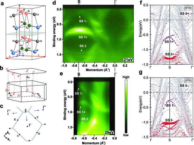
The crystal growth using a modified Bridgman–Stockbarger technique has been described in detail elsewhere Peets (2014). The crystals were cooled slowly through the phase transition to maximize the domain size of the low-temperature phase; resulting in high-quality crystals Peets et al. (2016). At low temperature -BiPd (in the following referred to as “BiPd”) forms in the noncentrosymmetric space group P21 Zhuravlev (1957); Bhatt and Schubert (1980, 1979); Ionov et al. (1989). The structure is characterized by two double layers stacked along the monoclinic axis, which are related by a 180∘ screw symmetry [see Fig. 1(a)]. Since the bonding between double layers is weaker than within them, the crystals readily cleave perpendicular to the monoclinic axis and, as previously demonstrated Sun et al. (2015), are twinned such that both (010) and (01̄0) surfaces can appear on the same side of the crystal (see ref. sup, for details on the cleaving procedure).
ARPES measurements were performed on freshly cleaved surfaces using (i) a Helium source ( and 40.8 eV) with a hemispherical SPECS HSA3500 electron analyzer, and (ii) linearly-polarized synchrotron light from the UE112-PGM undulator beamline at BESSY II with a Scienta R8000 analyzer. The sample was held at temperatures lower than 100 K during cleaving and throughout the measurements.
STM experiments were performed in a home-built low-temperature STM operating at temperatures down to in cryogenic vacuum Singh et al. (2013). Samples were prepared by in-situ cleaving at low temperatures. Tips were cut from a PtIr wire. Bias voltages were applied to the sample. Differential conductance spectra have been recorded through a lock-in amplifier (, ).
Figures 1(b) and (c) show schematically the bulk Brillouin zone and its surface projection. Figures 1(d) and (e) show the results of ARPES, measured along the –S direction in the Brillouin zone at two different photon energies. The most prominent feature of the surface electronic structure when measured with a He-I lamp is the appearance of a strong state (labelled SS1+ in Fig. 1(d)) at the S-point at 0.7 eV binding energy. In addition, at higher photon energy (Fig. 1(e)), within the same directional band gap at the S-point a surface state SS1– can be identified, albeit with much weaker intensity. These are identified as surface states through their lack of dispersion with varying the incident photon energy and hence sup . To understand the origin and topological nature of these surface states, we have employed fully relativistic linear muffin tin orbital calculations Andersen (1975); Antonov et al. (2004); Perlov et al. using a repeated slab system consisting of six BiPd double layers separated by two empty double layers which represent the vacuum. We find that around the Fermi energy , all the bands are mainly of Bi orbital character with subdominant but non-negligible contributions of Pd states. The strong atomic SOC of Bi induces a spin splitting of the bands of the order of tens of meV and, moreover, results in a large energy shift of states that have predominant orbital characterMacdonald et al. (1980). The latter leads to formation of a band gap at the point Sun et al. (2015); Macdonald et al. (1980). In Figs. 1(f) and (g), we show the calculated dispersions near of the (010) and (01̄0) surfaces of BiPd, respectively, along high symmetry directions of the surface BZ [Fig. 1(b) and (c)]. The momentum-resolved surface densities of states at the (010) and (01̄0) sides are indicated by filled circles. Interestingly, Dirac surface states appear both at the and points of the surface BZ. Thus by comparison with band structure calculations, the features SS1+ and SS1- seen in ARPES can be directly associated with the surface states of the BiPd surface. The simultaneous observation of SS1+ and SS1- in the measurement is not reproduced in the calculations: the two states originate from opposite surface terminations, with the one at higher binding energy arising from the (010) termination and the one closer to the Fermi energy from the (01̄0) termination. Since these two terminations correspond to opposite surfaces of a single crystal, their simultaneous observation by ARPES indicates twin domains with opposite direction of the crystallographic axis within the beam spot. A structural transition around 200∘C Bhatt and Schubert (1979); Ionov et al. (1989) is known to cause twinning, and this type of twin boundary has been previously observed by STM Sun et al. (2015).
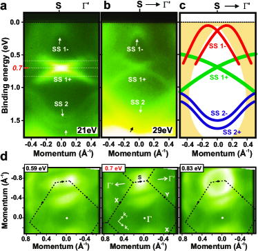
In full agreement between experiment and theory, the spin-splitting of the surface state is substantially larger in the S- direction compared to the S- direction. Experimental data for the S- direction are shown in Figs. 2(a) and (b), taken at the same photon energies as Figs. 1(d) and (e), respectively. The two measurements show the states SS1+ and SS1– with different intensities, but otherwise at the same energy and having the same dispersion, confirming that they are of two-dimensional character. The different intensities are likely due to final state effects. There are small differences in binding energies between experiment and calculation on the order of 100 meV. One likely source of this discrepancy is surface relaxation which is neglected in the calculation. Constant energy contours obtained at the energies around the Dirac point, shown in Fig. 2(d) for the energies labelled in Fig. 2(a), clearly reveal the two band maxima in the S- direction due to the strongly anisotropic Rashba splitting (see also Ref. sup, ).
Data and calculations yield a further set of surface states at higher binding energies, which we label SS2+ and SS2-. As opposed to the hole-like SS1 states, SS2 have an electron-like dispersion. In the experiment, they are most clearly resolved with (Fig. 2(a)). They are located near the bottom of the directional band gap at the S-point and quickly develop into surface resonances when moving away from .
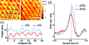
Besides the surface states found at the points, the calculations reveal an additional pair of surfaces states at the point (labelled by SS0 in Figs. 1(f) and (g)), which are in the unoccupied states and thus inaccessible to ARPES. For one termination, this state has been detected previously by STS Sun et al. (2015). While the Dirac-cone states at the point are present even if SOC is neglected, the Dirac state at the point appears within a gap opened up by SOC and arises as a consequence of an SOC-driven band inversion. This scenario is reminiscent of the topological insulator Bi2Se3 Xia et al. (2009), indicating a possible topological origin. Here we show the signature of the surface state at for both terminations from tunneling spectra, see Fig. 3. The terminations in the STM data have been identified from the surface corrugation (compare fig. 3(a-c)). Spectra of the surface state (fig. 3(d) show only a very small shift of between the two terminations, with the surface state showing up at larger energies on the termination which we identify as the (01̄0) surface.
We note that the band crossings of the Dirac states both at the and points are protected by time-reversal symmetry due to Kramers’ theorem. Consistently for all surface states in the occupied states (SS1, SS2) those on the (010) surface occur at an energy at least 100 meV higher than on (01̄0), whereas the shift is very small and in the opposite direction for the surface state in the unoccupied states (SS0).
We have fitted the standard Rashba-Bychkov model Bychkov and Rashba (1984) to cuts through the experimental band structure maps along the high-symmetry directions to extract the magnitude of spin splitting for the most prominent surface state, SS1+. The dispersion about the high-symmetry point is modeled as
| (1) |
where denotes the momentum along the chosen direction in the surface BZ, is the effective mass, and and denote the momentum offset and the energy of the band maxima, respectively. We quantify the size of the Rashba splitting by the momentum offset and the energy difference between the band maximum and the band crossing point. The fits used to extract these parameters for SS1+ are shown in Figs. 4(a) and (b) for the S– and S– directions, respectively. The Rashba momentum offset and energy along the S– direction in BiPd rank among the largest reported thus far, while both are significantly smaller in the S– direction. The results are summarized and compared with a selection of previously reported values in Table 1. Despite the large momentum offset, the Rashba parameter of BiPd is smaller than for the Bi/Ag(111) surface alloy due to the much larger effective mass of the surface states of BiPd. Large Rashba splittings, leading to well-separated spin-split bands, may prove useful for applications involving the transport of spin rather than charge. Interesting, the Figure 4(c) shows a three-dimensional representation of the dispersion of SS1+ near the S-point, highlighting the anisotropy in the Rashba spin-splitting.
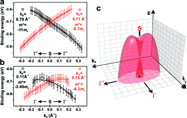
| Sample | Ref. | |||||
|---|---|---|---|---|---|---|
| Au(111) | 0. | 012 | 2.1 | 0. | 33 | LaShell et al.,1996 |
| Bi(111) | 0. | 05 | 14 | 0. | 55 | Koroteev et al.,2004 |
| Bi/Ag surface alloy | 0. | 13 | 200 | 3. | 05 | Ast et al.,2007 |
| BiTeI | 0. | 052 | 100 | 3. | 8 | Ishizaka et al.,2011 |
| BaNiS2 | 0. | 2 | 150 | 0. | 26 | Santos-Cottin et al.,2016 |
| BiPd SS1+, S– | 0. | 13 | 17 | 0. | 25 | this work |
| BiPd SS1+, S– | 0. | 75 | 208 | 0. | 55 | this work |
Since BiPd is noncentrosymmetric and no symmetry element can transform a (010) surface into a (01̄0) surface, the shapes and energies of these surfaces’ Dirac states can be quite different, and indeed this is what we observe.
Our data reveal a surprising richness of Dirac surface states on the (010)/(01̄0) surfaces of BiPd. Evidence for a surface state above at Sun et al. (2015) and the observation of surface state SS1+ have been recently reported Neupane et al. (2015) (although with a different assignment of the and points in the latter). From a detailed comparison of calculations, ARPES and STM data we can identify two distinct surface states below the Fermi level at the point and one at the point, on each surface. The data reveal signatures of surface states from opposite orientations of the cystallographic -axis, which occur on opposite faces of an ideal crystal, implying twinning on the scale of the ARPES spot size. Macroscopic studies of the impact of the lack of inversion symmetry on the material properties may therefore need to detwin the material to yield information from a single domain. The overall consistency of our results with the previously published data confirms the high reproducibility of the properties of BiPd.
The Rashba splitting of the surface states at the S-point exhibits a strong anisotropy, suggesting strongly directionally-dependent SOC in the surface state. This strong directional dependence can be understood by comparison with the surface structure of BiPd: the –S direction is along rows of Bi (or Pd) atoms, therefore electronic states propagating along this direction are only moderately exposed to the surface corrugation. Along the –S′ (or equivalently S–) direction, rows of Bi and Pd atoms alternate, and electronic states with wavevectors along this direction are exposed much more strongly to the surface corrugation and hence to the surface electric fields which generate the spin splitting. The connection between surface corrugation and the spin-orbit splitting has been discussed previously in the context of the Bi/Ag(111) surface alloy Gierz et al. (2010); Bian et al. (2013). In BiPd, the corrugation of the top-most layer is a direct consequence of the crystal structure of the bulk material, boosting the spin splitting of the surface states only in specific directions due to the anisotropy of the crystal structure.
In summary, through comparison of ARPES and STM experiments with band structure calculations, we have confirmed the presence of unconventional Dirac surface states in noncentrosymmetric BiPd. The extremely large and anisotropic Rashba splitting in this system makes it an excellent candidate for future studies on the intricate spin texture of spin-split bands. Our results suggest a new way to engineer anisotropic spin textures and Rashba splittings of surface states by exploiting the low symmetry of the surface termination. The findings provide independent confirmation of the existence of twin boundaries in the material Sun et al. (2015), which may prove crucial to understanding its superconducting properties Peets et al. (2016); Yan et al. (2016).
Acknowledgments.— The authors thank Ed Yelland for useful discussions. Funding from the MPG-UBC center and the Engineering and Physical Sciences Research Council (EP/I031014/1 and EP/L505079/1) are acknowledged. This work was supported by the DFG within projects STA315/8-1 and BE5190/1-1. We also thank the staff at Bessy II of the Helmholtz-Zentrum Berlin for their assistance.
References
- Hasan and Kane (2010) M. Z. Hasan and C. L. Kane, Rev. Mod. Phys. 82, 3045 (2010).
- Qi and Zhang (2011) X.-L. Qi and S.-C. Zhang, Rev. Mod. Phys. 83, 1057 (2011).
- Hasan and Moore (2011) M. Z. Hasan and J. E. Moore, Ann. Rev. Cond. Matt. Phys. 2, 55 (2011).
- Hsieh et al. (2009a) D. Hsieh, Y. Xia, L. Wray, D. Qian, A. Pal, J. H. Dil, J. Osterwalder, F. Meier, G. Bihlmayer, C. L. Kane, Y. S. Hor, R. J. Cava, and M. Z. Hasan, Science 323, 919 (2009a).
- Xia et al. (2009) Y. Xia, D. Qian, D. Hsieh, L. Wray, A. Pal, H. Lin, A. Bansil, D. Grauer, Y. S. Hor, R. J. Cava, and M. Z. Hasan, Nat Phys 5, 398 (2009).
- Seo et al. (2010) J. Seo, P. Roushan, H. Beidenkopf, Y. S. Hor, R. J. Cava, and A. Yazdani, Nature 466, 343 (2010).
- Rashba (1960) E. I. Rashba, Sov. Phys. Solid State 2, 1109 (1960).
- Ast et al. (2007) C. R. Ast, J. Henk, A. Ernst, L. Moreschini, M. C. Falub, D. Pacilé, P. Bruno, K. Kern, and M. Grioni, Phys. Rev. Lett. 98, 186807 (2007).
- Crepaldi et al. (2012) A. Crepaldi, L. Moreschini, G. Autès, C. Tournier-Colletta, S. Moser, N. Virk, H. Berger, P. Bugnon, Y. J. Chang, K. Kern, A. Bostwick, E. Rotenberg, O. V. Yazyev, and M. Grioni, Phys. Rev. Lett. 109, 096803 (2012).
- Bahramy et al. (2012) M. Bahramy, B.-J. Yang, R. Arita, and N. Nagaosa, Nat. Commun. 3, 679 (2012).
- Hsieh et al. (2009b) D. Hsieh, Y. Xia, D. Qian, L. Wray, J. H. Dil, F. Meier, J. Osterwalder, L. Patthey, J. G. Checkelsky, N. P. Ong, A. V. Fedorov, H. Lin, A. Bansil, D. Grauer, Y. S. Hor, R. J. Cava, and M. Z. Hasan, Nature 460, 1101 (2009b).
- Ishizaka et al. (2011) K. Ishizaka, M. S. Bahramy, H. Murakawa, M. Sakano, T. Shimojima, T. Sonobe, K. Koizumi, S. Shin, H. Miyahara, A. Kimura, K. Miyamoto, T. Okuda, H. Namatame, M. Taniguchi, R. Arita, N. Nagaosa, K. Kobayashi, Y. Murakami, R. Kumai, Y. Kaneko, Y. Onose, and Y. Tokura, Nat. Mater. 10, 521 (2011).
- Wang et al. (2011) Y. H. Wang, D. Hsieh, D. Pilon, L. Fu, D. R. Gardner, Y. S. Lee, and N. Gedik, Phys. Rev. Lett. 107, 207602 (2011).
- Bauer and Sigrist (2012) E. Bauer and M. Sigrist, Non-Centrosymmetric Superconductors: Introduction and Overview, Lecture Notes in Physics, Vol. 847 (Springer Berlin, 2012) pp. 1–357.
- Bauer et al. (2004) E. Bauer, G. Hilscher, H. Michor, C. Paul, E. W. Scheidt, A. Gribanov, Y. Seropegin, H. Noël, M. Sigrist, and P. Rogl, Phys. Rev. Lett. 92, 027003 (2004).
- Schnyder et al. (2008) A. P. Schnyder, S. Ryu, A. Furusaki, and A. W. W. Ludwig, Phys. Rev. B 78, 195125 (2008).
- Béri (2010) B. Béri, Phys. Rev. B 81, 134515 (2010).
- Schnyder and Ryu (2011) A. P. Schnyder and S. Ryu, Phys. Rev. B 84, 060504 (2011).
- Sato and Fujimoto (2009) M. Sato and S. Fujimoto, Phys. Rev. B 79, 094504 (2009).
- Kheiker et al. (1953) D. M. Kheiker, G. S. Zhdanov, and N. N. Zhuravlev, Zh. Eksp. Teor. Fiz. 25, 621 (1953).
- Zhuravlev (1957) N. Zhuravlev, Zh. Eksp. Teor. Fiz. 5, 1064 (1957).
- Bhatt and Schubert (1980) Y. Bhatt and K. Schubert, Journal of the Less Common Metals 70, P39 (1980).
- Bhatt and Schubert (1979) Y. Bhatt and K. Schubert, J. Less-Common Met. 64, P17 (1979).
- Ionov et al. (1989) V. M. Ionov, N. A. Tomilin, A. E. Prozorovskii, A. N. Klimenko, Y. V. Titov, S. G. Zhukov, and G. V. Fetisov, Sov. Phys. Crystallogr. 34, 496 (1989).
- Alekseevskii (1952) N. E. Alekseevskii, Zh. Eksp. Teor. Fiz. 23, 484 (1952).
- Joshi et al. (2011) B. Joshi, A. Thamizhavel, and S. Ramakrishnan, Phys. Rev. B 84, 064518 (2011).
- Mondal et al. (2012) M. Mondal, B. Joshi, S. Kumar, A. Kamlapure, S. C. Ganguli, A. Thamizhavel, S. S. Mandal, S. Ramakrishnan, and P. Raychaudhuri, Phys. Rev. B 86, 094520 (2012).
- Matano et al. (2013) K. Matano, S. Maeda, H. Sawaoka, Y. Muro, T. Takabatake, B. Joshi, S. Ramakrishnan, K. Kawashima, J. Akimitsu, and G.-q. Zheng, J. Phys. Soc. Jpn. 82, 084711 (2013).
- Sun et al. (2015) Z. Sun, M. Enayat, A. Maldonado, C. Lithgow, E. Yelland, D. C. Peets, A. Yaresko, A. P. Schnyder, and P. Wahl, Nat Commun 6, 6633 (2015).
- Peets et al. (2016) D. C. Peets, A. Maldonado, M. Enayat, Z. Sun, P. Wahl, and A. P. Schnyder, Phys. Rev. B 93, 174504 (2016).
- Sasaki et al. (2011) S. Sasaki, M. Kriener, K. Segawa, K. Yada, Y. Tanaka, M. Sato, and Y. Ando, Phys. Rev. Lett. 107, 217001 (2011).
- Levy et al. (2013) N. Levy, T. Zhang, J. Ha, F. Sharifi, A. A. Talin, Y. Kuk, and J. A. Stroscio, Phys. Rev. Lett. 110, 117001 (2013).
- Liu et al. (2011) C. Liu, Y. Lee, T. Kondo, E. D. Mun, M. Caudle, B. N. Harmon, S. L. Bud’ko, P. C. Canfield, and A. Kaminski, Phys. Rev. B 83, 205133 (2011).
- Kim et al. (2016) H. Kim, K. Wang, Y. Nakajima, R. Hu, S. Ziemak, P. Syers, L. Wang, H. Hodovanets, J. D. Denlinger, P. M. R. Brydon, D. F. Agterberg, M. A. Tanatar, R. Prozorov, and J. Paglione, “Beyond spin-triplet: Nodal topological superconductivity in a noncentrosymmetric semimetal,” (2016), arXiv:1603.03375 [cond-mat.supr-con] .
- Nakajima et al. (2016) Y. Nakajima, R. Hu, K. Kirshenbaum, A. Hughes, P. Syers, X. Wang, K. Wang, R. Wang, S. R. Saha, D. Pratt, J. W. Lynn, and J. Paglione, Sci. Adv. 1, e1500242 (2016).
- Ali et al. (2014) M. N. Ali, Q. D. Gibson, T. Klimczuk, and R. J. Cava, Phys. Rev. B 89, 020505 (2014).
- Bian et al. (2016) G. Bian, T.-R. Chang, R. Sankar, S.-Y. Xu, H. Zheng, T. Neupert, C.-K. Chiu, S.-M. Huang, G. Chang, I. Belopolski, D. S. Sanchez, M. Neupane, N. Alidoust, C. Liu, B. Wang, C.-C. Lee, H.-T. Jeng, C. Zhang, Z. Yuan, S. Jia, A. Bansil, F. Chou, H. Lin, and M. Z. Hasan, Nat. Commun. 7, 10556 (2016).
- Guan et al. (2016) S.-Y. Guan, P.-J. Chen, M.-W. Chu, R. Sankar, F. Chou, H.-T. Jeng, C.-S. Chang, and T.-M. Chuang, “Superconducting topological surface states in non-centrosymmetric bulk superconductor PbTaSe2,” (2016), arXiv:1605.00548 [cond-mat.supr-con] .
- Neupane et al. (2015) M. Neupane, N. Alidoust, S.-Y. Xu, I. Belopolski, D. S. Sanchez, T.-R. Chang, H.-T. Jeng, H. Lin, A. Bansil, D. Kaczorowski, M. Z. Hasan, and T. Durakiewicz, “Discovery of the topological surface state in a noncentrosymmetric superconductor BiPd,” (2015), arXiv:1505.03466 [cond-mat.mes-hall] .
- Peets (2014) D. C. Peets, J. Phys.: Conf. Ser. 568, 022037 (2014).
- (41) See Supplemental Material at http://link.aps.org/ supplemental/10.1103/ for additional ARPES measurements.
- Singh et al. (2013) U. Singh, M. Enayat, S. White, and P. Wahl, Rev. Sci. Instr. 84, 013708 (2013).
- Andersen (1975) O. K. Andersen, Phys. Rev. B 12, 3060 (1975).
- Antonov et al. (2004) V. Antonov, B. Harmon, and A. Yaresko, Electronic structure and magneto-optical properties of solids (Kluwer Academic Publishers, Dordrecht, Boston, London, 2004).
- (45) A. Y. Perlov, A. N. Yaresko, and V. N. Antonov, PY-LMTO: A Spin-Polarized Relativistic LMTO Package for Electronic Structure Calculations (unpublished).
- Macdonald et al. (1980) A. H. Macdonald, W. E. Pickett, and D. D. Koelling, J. Phys. C 13, 2675 (1980).
- Bychkov and Rashba (1984) Y. A. Bychkov and É. I. Rashba, JETP Lett. 39, 78 (1984).
- LaShell et al. (1996) S. LaShell, B. A. McDougall, and E. Jensen, Phys. Rev. Lett. 77, 3419 (1996).
- Koroteev et al. (2004) Y. M. Koroteev, G. Bihlmayer, J. E. Gayone, E. V. Chulkov, S. Blügel, P. M. Echenique, and P. Hofmann, Phys. Rev. Lett. 93, 046403 (2004).
- Santos-Cottin et al. (2016) D. Santos-Cottin, M. Casula, G. Lantz, Y. Klein, L. Petaccia, P. Le Fèvre, F. Bertran, E. Papalazarou, M. Marsi, and A. Gauzzi, Nat. Commun. 7, 11258 (2016).
- Gierz et al. (2010) I. Gierz, B. Stadtmüller, J. Vuorinen, M. Lindroos, F. Meier, J. H. Dil, K. Kern, and C. R. Ast, Physical Review B 81, 245430 (2010).
- Bian et al. (2013) G. Bian, X. Wang, T. Miller, and T.-C. Chiang, Physical Review B 88, 085427 (2013).
- Yan et al. (2016) X. B. Yan, Y. Xu, L. P. He, J. K. Dong, H. B. Cho, D. C. Peets, J.-G. Park, and S. Y. Li, Supercond. Sci. Tech. 29, 065001 (2016).
Supplementary Information for
“Observation of Dirac surface states in the noncentrosymmetric superconductor BiPd”
H. M. Benia, E. Rampi, C. Trainer, C. M. Yim, A. Maldonado, D. C. Peets, A. Stöhr, U. Starke, K. Kern, A. Yaresko, G. Levy, A. Damascelli, C. R. Ast, A. P. Schnyder, and P. Wahl
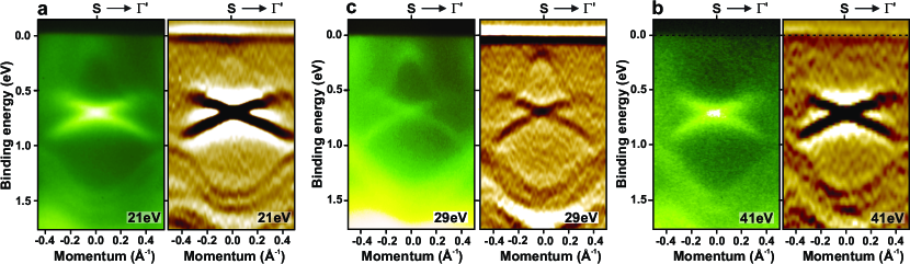
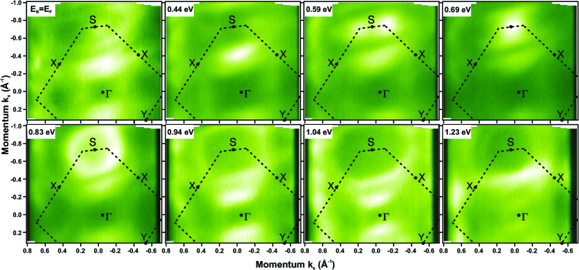
Figures S1 and S2 show supporting ARPES data. In Fig. S1 ARPES intensity maps are displayed for three different incident photon energies. These energies probe different , leading to rather different bulk band structures in this relatively three-dimensional material, but the two-dimensional surface states do not disperse. This figure also includes second-derivative images, showing the surface states with greater contrast. Figure S2 shows additional constant-energy cuts for an incident photon energy of 21 eV, fleshing out the dispersion of the surface states in greater detail.
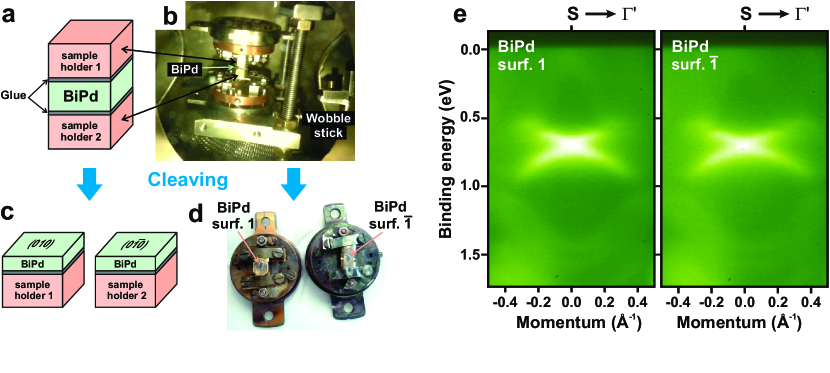
Figure S3 shows the cleaving setup that was used to obtain surfaces with opposite surface termination. Since the ARPES measurements of the two cleaved surfaces exhibit similar features, we conclude that the BiPd crystal consists of twin domains, with the twin domain size smaller than the ARPES beam spot.