Donors in Ge as Qubits – Establishing Physical Attributes
Abstract
Quantum electronic devices at the single impurity level demand an understanding of the physical attributes of dopants at an unprecedented accuracy. Germanium-based technologies have been developed recently, creating a necessity to adapt the latest theoretical tools to the unique electronic structure of this material. We investigate basic properties of donors in Ge which are not known experimentally, but are indispensable for qubit implementations. Our approach provides a description of the wavefunction at multiscale, associating microscopic information from Density Functional Theory and envelope functions from state of the art multivalley effective mass calculations, including a central cell correction designed to reproduce the energetics of all group V donor species (P, As, Sb and Bi). With this formalism, we predict the binding energies of negatively ionized donors (D- state). Furthermore, we investigate the signatures of buried donors to be expected from Scanning Tunneling Microscopy (STM). The naive assumption that attributes of donor electrons in other semiconductors may be extrapolated to Ge is shown to fail, similar to earlier attempts to recreate in Si qubits designed for GaAs. Our results suggest that the mature techniques available for qubit realizations may be adapted to germanium to some extent, but the peculiarities of the Ge band structure will demand new ideas for fabrication and control.
I Introduction
Single donor electronics, fully governed by quantum mechanics, is now accessible due to progress in sample fabrication and characterization Fuechsle et al. (2012); Verduijn et al. (2013); Zwanenburg et al. (2013); Koenraad and Flatté (2011). Advances in the study of isolated donors in Si naturally motivate investigations in Ge along similar paths Scappucci et al. (2015). Atomically precise fabrication of devices based on STM litography have been demonstrated Scappucci et al. (2011), paving the road for future applications such as quantum computation. Indeed, germanium shares many of the interesting properties of Si, such as the low abundance of isotopes with nuclear spin in the natural material. This leads to microseconds long coherence of electron spins Sigillito et al. (2015), which has been extended up to milliseconds in isotopically purified samples. More recent results also point towards feasible Stark tuning of the electron spin resonance, which may serve as a scheme for individual dopant control Sigillito et al. (2016). But unlike silicon-based technologies, current knowledge about the physics of electrons in Ge is limited. Experimental determination of negatively-charged ionic states– known to play an important role in nanoscopic devices – is lacking. The theoretical description of the electronic wavefunction at the atomic level is also incomplete.
We present here a comprehensive investigation for isolated donor-based qubits in Ge with one and two electrons. Our model incorporates parameters which consistently reproduce and predict specific fingerprints for substitutional P, As, Sb and Bi dopants. Calculated ground state energies for neutral ()and negatively ionized () donors, binding and charging energies are in good agreement with experiments; and when experimental values are not available, suitable estimates are given. Combining multivalley effective-mass Kohn-Luttinger (KL) envelopes Kohn and Luttinger (1955) and ab-initio calculated Bloch functions at the points, we simulate sub-surface donor images to be expected in STM experiments on a [001] surface, providing additional probes on the presence and location of sub-surface donors in Ge. The multiscale nature of our approach is made necessary by the variety of length scales that appear in this problem, ranging from the sub-nanometer central cell potential to the loosely confined wavefunction of the ionic state, which spreads over tens of lattice parameters.
Recent donor image studies in Si Saraiva et al. (2016) reveal the unsuspected adequacy of the KL ground state wave function to describe donors’ signatures probed at a surface a few monolayers above it. The prominent role played by the host material atomic arrangement and conduction band structure is also discussed in Ref. Saraiva et al., 2016. Although Ge is also a group IV element and shares the same crystal structure of Si (the diamond structure), the conduction band minima of Ge lie at 4 nonequivalent L points. This leads to dopant signatures in Ge that are very distinct from those of Si. Density Functional Theory calculations provide plane wave expansion coefficients for the Bloch functions of a set of four inequivalent -points.
II Formalism
The original effective mass equation for shallow donors in Ge incorporates the conduction band mass anisotropy ( in units of the bare electron mass ) and a screened Coulomb potential (), but not the band edge degeneracy Dresselhaus (2001). For Ge, within the Kohn-Luttinger single valley approach (KLSV), the calculated energy of an electron in the ground state is meV, regardless of the donor species. For energetics, we may further simplify the single valley formalism by assuming the band is isotropic, characterized by a single mass consistently chosen so that the ground state energy equals the KLSV value, i.e. which gives in units of . This calculation also leads to the hydrogenic approximation for the wavefunction radius nm. On the other hand, for wavefunction calculations below we take the mass anisotropy into account.
Experimentally, the ground state binding energies of group V donors in Ge are larger than , ranging from to meV. This is expected, since inter-valley coupling mediated by the impurity perturbation potential is not explicitly included in the single valley formalism. Within the isotropic band assumption, we take the impurity potential as , in which we include a central-cell contribution which correctly reproduces the behavior of screening for and , given by
| (1) |
The donor-specific empirical parameter is a crossover length between the short and long-range behavior of the potential and it completely defines the central-cell-corrected hamiltonian. It is chosen from a variational calculation by assuming hydrogenic envelopes of the form , taking the effective Bohr radius as the variational parameter. We take so that the variational and experimental ground state energies match: .
In Table 1, we give the values of and for P, As, Sb and Bi donors at the neutral state in Ge. Note that is over one order of magnitude smaller than for all donors, thus indicating that the central cell correction is only relevant within a narrow region around the donor site.
The effects of the intervalley coupling on the energetics of neutral donors can be incorporated in our single valley formalism in the following way. Within the KL multivalley effective mass theory Kohn and Luttinger (1955), the wavefunction of a neutral donor in Ge can be described in terms of s-like envelopes combined with the Ge Bloch functions at the four band minima:
| (2) |
where the index runs over four nonequivalent L points and denotes the periodic part of the corresponding Bloch function. Intervalley coupling in Ge lifts the fourfold degeneracy (energy ) into a non-degenerate ground state and three degenerate excited states . Each of these states is characterized by different coeficients on Eq. (2).
It can be easily verified that the energies of the and states may be written as and , where is the first order correction to the single valley energies and . The two shift parameters and are obtained by matching the theoretical and experimental values of and , thus allowing the incorporation of the energy splitting into our description, where only one isotropic envelope is involved. Table 1 shows the shift and central cell parameters, and the energies of the and states for neutral As, P, Sb and Bi donors. The experimental and theoretical results in this table are, therefore, designed to match accurately. From these results we can make new predictions, as we discuss below.
| D0 | P0 | As0 | Sb0 | Bi0 |
|---|---|---|---|---|
| acc | ||||
| rcc | ||||
| A | ||||
| T | ||||
| A | ||||
| T |
III Binding and Charging Energies
We turn our attention to the negatively charged donor state. Here we follow an analogy with the H- and He problems in atomic physics Bethe and Salpeter (2008), as described in Ref. Saraiva et al. (2015). Within the isotropic single valley model, the two-electron Hamiltonian is written as:
| (3) |
where is the kinetic energy operator for electron , is the central-cell corrected donor potential for electron and the last term is the Coulomb repulsion between the electrons. For the impurity potentials, we use the same expressions and values of obtained from the neutral donor state calculations, as given by Table 1.
The energy is obtained variationally by assuming that the two-electron wavefunction is a symmetric combination of envelopes Bethe and Salpeter (2008)
| (4) |
where and , represent the effective Bohr radii of inner and outer orbitals, taken as variational parameters. The values of , and of the variational energy are given in Table 2.
Notice that may be as large as 16 nm and is strongly impacted by the central cell potential, which is present at the scale of nm. To describe physical attributes at such wide range of length scales requires a multiscale description such as the one developed here.
From the energy and the energy of the state , we estimate the binding and charging energies as and , respectively. Those energies are also reported in Table 2, together with experimental data, available only for As- and Sb-. Since our model for the state does not include any additional empirical parameters, the good agreement with available experiments certifies the consistency of our model, thus indicating that the values for and for P- and Bi- in Table 2 are probably reliable estimates.
| D- | P- | As- | Sb- | Bi- |
|---|---|---|---|---|
| ai | ||||
| ao | ||||
| E | NA | NA | ||
| E | ||||
| E | NA | NA | ||
| E | ||||
| UExp | NA | NA | ||
| UCalc |
IV Subsurface Donor Signature
Fingerprints of subsurface donors in semiconductors are now accessible from STM images Koenraad and Flatté (2011). Recent scans on a (001) surface in Si Salfi et al. (2014) identify the presence of buried donors, with a charge distribution aligned along the direction defined by the surface dimerization. The overall appearance of the STM images of donors in Si were satisfactorily described by a model that assumes that the tunnel current is proportional to the local electronic density of states; the STM tip is kept at a constant height from the surface; and the electronic charge distribution near a surface shows negligible changes due to the presence of the surface, keeping the corresponding bulk features. In fact the simulated images adopted in comparison to the STM images are merely two-dimensional cuts of the KL multivalley density through interstitial lattice planes Saraiva et al. (2016). Similar measurements are being performed in Ge:P with increasing level of refinement Scappucci et al. (2009); Mattoni et al. (2013), leading to the expectation that a complete profile of the impurity charge density will soon be available. For this reason we explore, within the same assumptions, images to be expected from such measurements in Ge. We may also adopt the dimer row direction as a reference for the alignment of charge distributions in Ge.
For the Ge donor ground state, the general expression in Eq. (2) takes coefficients for all . The envelope functions will now include the effects of mass anisotropy. We choose the cartesian axis along the three cubic crystal directions in Ge. For a simple donor, the envelope for the minimum along , with , is written as
| (5) | |||||
where , and are the longitudinal and transverse effective Bohr radii and is the normalization constant. By using the experimental data from Ref. Madelung, 2004, we obtain ; for Ge. Central-cell corrected values are estimated by rescaling those values by the same factor obtained in the spherical approximation above (e.g., for a P donor the scaling factor is ).
Following the usual approach in ab-initio calculations, we identify the Bloch wavefunctions with the corresponding Kohn-Sham wavefunctions from Density Functional Theory Hohenberg and Kohn (1964); Kohn and Sham (1965). They were obtained here from an ab-initio calculation using the Quantum Espresso code Giannozzi et al. (2009). The periodic part of the Bloch wavefunction is expanded in plane waves as , where the summation runs over all reciprocal lattice vectors up to an energy cutoff of Ry. 111In the DFT calculation, we use a PZ-LDA exchange-correlation functional for the electron-electron interactions Perdew and Zunger (1981). The Brillouin Zone is sampled with a 12 x 12 x 12 Monkhorst-Pack k-point grid Monkhorst and Pack (1976). For the electron-ion interaction, we use a LDA-1/2 BHS norm-conserving scalar relativistic pseudopotential Bachelet et al. (1982); Ferreira et al. (2011), for which the equilibrium lattice constant is Å. Table 3 gives the complex coefficients for vectors such that . All coefficients are given in the Supplementary Material sup .
| Re | Im | ||||
|---|---|---|---|---|---|
| 1 | -1 | -1 | 0.320983 | -0.132956 | 0.121 |
| -1 | 1 | -1 | 0.320983 | -0.132956 | 0.121 |
| -1 | -1 | 1 | 0.320983 | -0.132956 | 0.121 |
| 0 | 0 | -2 | 0.320983 | 0.132956 | 0.121 |
| 0 | -2 | 0 | 0.320983 | 0.132956 | 0.121 |
| -2 | 0 | 0 | 0.320983 | 0.132956 | 0.121 |
| 0 | 0 | 0 | -0.110811 | 0.267521 | 8.38E-2 |
| -1 | -1 | -1 | -0.110811 | -0.267521 | 8.38E-2 |
| 1 | 1 | -1 | 4.4389E-2 | 0.107165 | 1.35E-2 |
| 1 | -1 | 1 | 4.4389E-2 | 0.107165 | 1.35E-2 |
| -1 | 1 | 1 | 4.4389E-2 | 0.107165 | 1.35E-2 |
| 0 | -2 | -2 | 4.4389E-2 | -0.107165 | 1.35E-2 |
| -2 | 0 | -2 | 4.4389E-2 | -0.107165 | 1.35E-2 |
| -2 | -2 | 0 | 4.4389E-2 | -0.107165 | 1.35E-2 |
| 1 | 1 | 1 | -6.6843E-2 | 2.7687E-2 | 5.23E-3 |
| -2 | -2 | -2 | -6.6843E-2 | -2.7687E-2 | 5.23E-3 |
Experimentally, donor images are collected by an STM tip kept at a fixed distance above the surface atomic plane. We fix the distance of the STM collected image to the surface to be , so that the predicted image is a cut through the electronic density at intersticial planes mid-way between consecutive Ge atomic planes, located at heights above the donor plane ( Ge lattice parameters and monoatomic planes, defining 4 inequivalent relative positions of the interface plane with respect to the donor) Saraiva et al. (2016). Interstitial plane cuts for the KL charge distributions for neutral P donors in Ge, in the sequence for , are given in Fig. 1. These images should emulate images to be expected in STM signatures of sub-surface donors in Ge. Atomic plane cuts (not shown here) produce very different images, which are not observable for the STM tip standing above such planes.
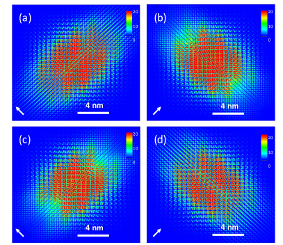
There is a marked change in the patterns from atomic planes to interstitial planes.
The simulated images of burried donors in Ge (Fig. 1) show elongated but almost featureless shapes, where the elongated axis is consistently perpendicular to the underlying dimer rows in Ge, alternating between the 2 possible dimerization directions. In comparison to donors in Si, where distinct shapes characterize successive monolayers, no noticeable differences appear between the four inequivalent relative positions of the Ge (001) surface plane and the impurity, namely . Moreover, the images shown here for a given depth of the donor in Ge spread over a considerably larger area at the surface, with linear dimensions typically twice as those of Si.
All interstitial distributions are elongated in the (frames a and c) or (frames b and d) surface directions. This behavior is independent of the unit cell : a cyclic sequence results for interstitial planes along the direction, and is related to the cyclic directional orientation of the zig-zag atomic rows in the diamond structure Saraiva et al. (2016). The larger spread of the donor electron in Ge in comparison with Si is a consequence of the lighter effective mass for an electron in Ge, thus larger Bohr radii (for example nm for P in Ge and nm for P in Si Saraiva et al. (2015)). Thus, comparatively, images in Ge appear fuzzy and featureless. A new feature that appears here is that the overall shape of the distributions remains constant for different depths of the substitutional donor with respect to the [100] surface. This is a consequence of the four L points being symmetrically oriented with the surface plane. In the case of Si, the lines perpendicular to the surface are not equivalent to the parallel ones, resulting in shapes readily identifiable (butterfly and caterpillar in Ref. Saraiva et al., 2016). One could expect differentiated images in Ge for [110] or [111] surfaces, which are not investigated here.
V Implications to Qubit Fabrication
While Ge-based quantum computer design may benefit from the knowledge of multivalley electronic structure acquired by the Silicon qubit community, many quantitative aspects of the spectrum and wavefunction of dopants are unique to germanium. Its exceptionally large dielectric constant and low electronic effective mass lead to very spread charge distributions, which could potentially facilitate the tunneling of electron to and from such dopants. If this is the main task for a given qubit design, our calculations indicate that Sb donors are particularly suitable, with a wavefunction spreading over more than 4 nm.
On the other hand, the binding of a second electron to the dopant, forming a D- state, is not naturally strong (hundreds of eV). This indicates that this state should not be stable in bulk at high temperatures, but can be made stable in nanostructures (specially near metals where the image charge generates some attractive potential Calderon et al. (2010)) or by implanting donors by pairs Gonzalez-Zalba et al. (2014). This is important in some proposals for spin manipulation based on spin-charge conversion. Donors in two-electron configurations have also been proposed to promote entanglement between nucleus-electron spin qubits Skinner et al. (2003). These ideas should be easier to implement with arsenic donors for a stronger binding of the second electron.
The wavefunction oscillation pattern due to the interference among Bloch states of the conduction band minima in Ge leads to a unique signature that might be exploited to identify these dopants from STM measurement. Yet, the fast oscillations might impair the use of these images for a complete three-dimensional determination of the donor position – unlike in silicon, where the charge distribution presents coarse signatures of the sublattice in which the substitutional donor is placed. A finer comparison between the oscillatory pattern from theory and the tunneling current might overcome this limitation, but an even more accurate description of the wavefunction may be required.
These physical attributes indicate that germanium can be superior to silicon for some tasks required for quantum applications, but not all. It is clear, though, that many procedures conceived for silicon architectures are readily transferable to Ge devices, which should stimulate further experimental progress for Ge-based qubits.
VI Acknowledgments
This work was performed as part of the Brazilian National Institute for Science and Technology on Quantum Information. We also acknowledge partial support from the Brazilian agencies FAPERJ, CNPq, CAPES.
References
- Fuechsle et al. (2012) M. Fuechsle, J. A. Miwa, S. Mahapatra, H. Ryu, S. Lee, O. Warschkow, L. C. L. Hollenberg, G. Klimeck, and M. Y. Simmons, Nature Nanotechnology 7, 242 (2012).
- Verduijn et al. (2013) J. Verduijn, G. C. Tettamanzi, and S. Rogge, Nano Letters 13, 1476 (2013).
- Zwanenburg et al. (2013) F. A. Zwanenburg, A. S. Dzurak, A. Morello, M. Y. Simmons, L. C. L. Hollenberg, G. Klimeck, S. Rogge, S. N. Coppersmith, and M. A. Eriksson, Reviews of Modern Physics 85, 961 (2013).
- Koenraad and Flatté (2011) P. M. Koenraad and M. E. Flatté, Nature Materials 10, 91 (2011).
- Scappucci et al. (2015) G. Scappucci, W. M. Klesse, L. A. Yeoh, D. J. Carter, O. Warschkow, N. A. Marks, D. L. Jaeger, G. Capellini, M. Y. Simmons, and A. R. Hamilton, Scientific reports 5 (2015).
- Scappucci et al. (2011) G. Scappucci, G. Capellini, B. Johnston, W. M. Klesse, J. A. Miwa, and M. Y. Simmons, Nano Letters 11, 2272 (2011), pMID: 21553900, http://dx.doi.org/10.1021/nl200449v .
- Sigillito et al. (2015) A. J. Sigillito, R. M. Jock, A. M. Tyryshkin, J. W. Beeman, E. E. Haller, K. M. Itoh, and S. A. Lyon, Phys. Rev. Lett. 115, 247601 (2015).
- Sigillito et al. (2016) A. J. Sigillito, A. M. Tyryshkin, J. W. Beeman, E. E. Haller, K. M. Itoh, and S. A. Lyon, arXiv 1606.0331 (2016).
- Kohn and Luttinger (1955) W. Kohn and J. M. Luttinger, Physical Review 98, 915 (1955).
- Saraiva et al. (2016) A. L. Saraiva, J. Salfi, J. Bocquel, B. Voisin, S. Rogge, R. B. Capaz, M. Calderón, and B. Koiller, Phys Rev B 93, 045303 (2016).
- Dresselhaus (2001) M. S. Dresselhaus, Solid Sate Physics, Part I, Transport Properties of Solids (MIT Press, 2001).
- Bethe and Salpeter (2008) H. Bethe and E. Salpeter, Quantum mechanics of one and two electron atoms (Dover publications, NY, 2008).
- Saraiva et al. (2015) A. L. Saraiva, A. Baena, M. J. Calderón, and B. Koiller, Journal of Physics: Condensed Matter 27, 154208 (2015).
- Pajot and Clerjaud (2012) B. Pajot and B. Clerjaud, Optical Absorption of Impurities and Defects in Semiconducting Crystals (Springer Science Bussines Media, 2012).
- Salfi et al. (2014) J. Salfi, J. A. Mol, R. Rahman, G. Klimeck, M. Y. Simmons, L. C. L. Hollenberg, and S. Rogge, Nature Materials 13, 605 (2014).
- Scappucci et al. (2009) G. Scappucci, G. Capellini, and M. Simmons, Physical Review B 80, 233202 (2009).
- Mattoni et al. (2013) G. Mattoni, W. M. Klesse, G. Capellini, M. Y. Simmons, and G. Scappucci, ACS nano 7, 11310 (2013).
- Madelung (2004) O. Madelung, Semiconductors: Data Handbook (Springer, 2004).
- Hohenberg and Kohn (1964) P. Hohenberg and W. Kohn, Physical Review 136, B864 (1964).
- Kohn and Sham (1965) W. Kohn and L. J. Sham, Physical Review 140, A1133 (1965).
- Giannozzi et al. (2009) P. Giannozzi, S. Baroni, N. Bonini, M. Calandra, R. Car, C. Cavazzoni, D. Ceresoli, G. L. Chiarotti, M. Cococcioni, I. Dabo, A. D. Corso, S. de Gironcoli, S. Fabris, G. Fratesi, R. Gebauer, U. Gerstmann, C. Gougoussis, A. Kokalj, M. Lazzeri, L. Martin-Samos, N. Marzari, F. Mauri, R. Mazzarello, S. Paolini, A. Pasquarello, L. Paulatto, C. Sbraccia, S. Scandolo, G. Sclauzero, A. P. Seitsonen, A. Smogunov, P. Umari, and R. M. Wentzcovitch, Journal of Physics: Condensed Matter 21 (2009).
- Note (1) In the DFT calculation, we use a PZ-LDA exchange-correlation functional for the electron-electron interactions Perdew and Zunger (1981). The Brillouin Zone is sampled with a 12 x 12 x 12 Monkhorst-Pack k-point grid Monkhorst and Pack (1976). For the electron-ion interaction, we use a LDA-1/2 BHS norm-conserving scalar relativistic pseudopotential Bachelet et al. (1982); Ferreira et al. (2011), for which the equilibrium lattice constant is Å.
- (23) See supplementary material for a complete list of the expansion coefficients partially given in Table 3. This list follows the same pattern of Table 3 and the coefficients for the other points can be readily obtained by using the transformations given in the caption of that Table.
- Calderon et al. (2010) M. Calderon, J. Verduijn, G. Lansbergen, G. Tettamanzi, S. Rogge, and B. Koiller, Physical Review B(Condensed Matter and Materials Physics) 82 (2010).
- Gonzalez-Zalba et al. (2014) M. F. Gonzalez-Zalba, A. Saraiva, M. J. Calderón, D. Heiss, B. Koiller, and A. J. Ferguson, Nano Letters 14, 5672 (2014).
- Skinner et al. (2003) A. J. Skinner, M. E. Davenport, and B. E. Kane, Physical Review Letters 90, 087901 (2003).
- Perdew and Zunger (1981) J. P. Perdew and A. Zunger, Physical Review B 23, 5048 (1981).
- Monkhorst and Pack (1976) H. J. Monkhorst and J. D. Pack, Physical Review B 13, 5188 (1976).
- Bachelet et al. (1982) G. B. Bachelet, D. R. Hamann, and M. Schlüter, Physical Review B 26, 4199 (1982).
- Ferreira et al. (2011) L. G. Ferreira, M. Marques, and L. K. Teles, AIP Advances 1, 032119 (2011).