Prominent metallic surface conduction and the singular magnetic response of topological Dirac fermion in three-dimensional topological insulator Bi1.5Sb0.5Te1.7Se1.3
Abstract
We report semiconductor to metal-like crossover in temperature dependence of resistivity () due to the switching of charge transport from bulk to surface channel in three-dimensional topological insulator Bi1.5Sb0.5Te1.7Se1.3. Unlike earlier studies, a much sharper drop in () is observed below the crossover temperature due to the dominant surface conduction. Remarkably, the resistivity of the conducting surface channel follows a rarely observable dependence at low temperature as predicted theoretically for a two-dimensional Fermi liquid system. The field dependence of magnetization shows a cusp-like paramagnetic peak in the susceptibility () at zero field over the diamagnetic background. The peak is found to be robust against temperature and decays linearly with field from its zero-field value. This unique behavior of is associated with the spin-momentum locked topological surface state of Bi1.5Sb0.5Te1.7Se1.3. The reconstruction of surface state with time is clearly reflected through the reduction of peak height with the age of the sample.
Topology protected electronic band structure is of current interest in condensed matter and material science research. Three-dimensional (3D) topological insulator has been established as an important member of this family since its first realization in Bi1-xSbxHeish and in binary compounds such as Bi2Se3Xia , Bi2Te3, Sb2Te3HD , etc. This class of ‘insulators’, due to strong spin-orbit coupling, hosts a metallic surface state with unique physical properties hasan . The spin-momentum locked surface state, which is protected by the time-reversal symmetry, makes the electronic transport robust against inelastic backscatteringhasan ; qi . Theoretical investigations have predicted them as potential candidates for applications in spintronics, quantum computation, etcqi . However, the above mentioned topological insulators reported to exhibit high bulk conductivity, instead of a gap between the valance and conduction band eto ; qu ; dutta ; Hor . It is now well documented that crystal defects - namely antisite defects and vacancies, which introduce large residual carriers, are the main reasons behind such high conductivity of the bulk Hor ; Taskin ; Ren . As a result, the transport response is dominated by the bulk rather than the surface. The misplacement of Se atom from its lattice position causes an increase in negative carrier concentration, which can be as high as 1019 cm-3, whereas the antisite defect of Bi and Sb produces holes Ren . Thus by replacing Bi with Sb and Se with Te in a proper ratio, one can balance the opposite type of carriers and minimize the conductivity. In order to achieve the higher figure of merit, efforts have been made to decrease the carrier density in the bulk by using ternary and quaternary compounds of Bi, Sb, Te and Se Ren ; shekhar . Teramoto and Takayanagi, in their work, reported that high resistivity can be obtained for compounds with chemical formula Bi2-xSbxTe3-ySey (BSTS) for a certain linear relation between and Teramoto . Ren et al. reinvestigated the electronic and structural phase diagram to achieve the intrinsic topological insulating state in these compounds and prescribed that the highest resistivity can be realised close to composition Bi1.5Sb0.5Te1.7Se1.3 Ren . Since then BSTS has been studied by various groups through transport Ren ; Ko ; Fran ; Taskin ; Segawa ; Lee ; Pan ; Hsiung and spectroscopic measurementsArakane ; Kim ; Ko ; Post ; Fran .
Topological insulators are characterised by their symmetry protected novel surface state properties. However, to observe high quality surface state property, one needs to electronically decouple the surface from the bulk. This can be achieved, by making the bulk highly insulating. We have grown high quality single crystals of topological insulators with composition Bi1.5Sb0.5Te1.7Se1.3. The bulk resistivity of some of the crystals used in the present study is about an order of magnitude larger than earlier reports Ren ; Ko ; Fran ; Taskin ; Segawa ; Lee ; Pan ; Hsiung . Notably, resistivity at low temperature decreases quadratically with temperature which is a clear evidence of Fermi liquid behavior of the surface state. Furthermore, the field dependence of susceptibility () exhibits an unusual paramagnetic peak at zero field as an evidence of the spin-momentum locked Dirac cone surface state.
Results
Temperature dependence of resistivity of Bi1.5Sb0.5Te1.7Se1.3 single crystals. The temperature dependence of resistivity () for three freshly cleaved Bi1.5Sb0.5Te1.7Se1.3 single crystals (S1,S2,S3) are presented in Fig. 1(a). Two slightly different techniques were used to prepare these single crystals. Crystal S3 was prepared by method I while crystals S1 and S2 were prepared by method II. The details of preparation are described in the Method section. With decreasing temperature, resistivity initially increases rapidly and then either decreases or tends to saturate. Overall, is larger for the crystals S1 and S2 as compared to S3. For example, for sample S2 is about 0.7 cm at 300 K and it increases with decreasing temperature and reaches a maximum of 42 cm at 40 K. On the other hand, at 300 K is an order of magnitude smaller and () shows a saturation-like behavior at low temperature for sample S3. Though the crystals S1 and S2 were prepared by the same method, the value and dependence of for these crystals are slightly different. Ren et al. also reported sample dependence of which they attributed to small variation in defect concentration in their samples Ren . For a given nominal composition, they observed to vary by a factor of 3 Ren . Both the value and dependence of for sample S3 are similar to earlier reports Ren ; Taskin . In a usual electrical transport measurement, as the bulk and surface resistance are in parallel configuration, they contribute simultaneously to conductivity. However, their relative contribution is sensitive to temperature. Due to the two-dimensional (2D) nature of the surface state, the cross section area of the conducting channel is extremely small. For this reason, the surface resistance can be significantly larger as compared to semiconducting bulk specially at high temperatures. Thus, the charge conduction at high temperature is dominated by the bulk. With decrease in temperature, the bulk resistance increases exponentially whereas the surface resistance decreases. This kind of temperature dependence of bulk and surface resistance results in a semiconductor to metal-like crossover at low temperature below which the charge transport is dominated by the surfaceTaskin ; Lee ; Fran ; Ko ; Pan . For both technological application and basic research, it is desirable that the bulk conductivity should be very small while the surface conductivity should be high. Several attempts have been made to achieve low bulk conductivity. Most of the reported data on single crystals show that exhibits the expected semiconducting behavior at high temperature. However, at low temperature, becomes either -independent or shows a very weak temperature dependence, i.e., the system is barely metallic. Also, the maximum value of resistivity is few cm only. for S1 and S2 samples at semiconductor to metal-like crossover temperature is an order of magnitude larger than those reported by several groupsRen ; Taskin ; Lee ; Pan and falls rapidly with decreasing temperature down to 2 K. To the best of our knowledge, such a strong decrease in surface-state resistance with decreasing temperature has not been observed so far.
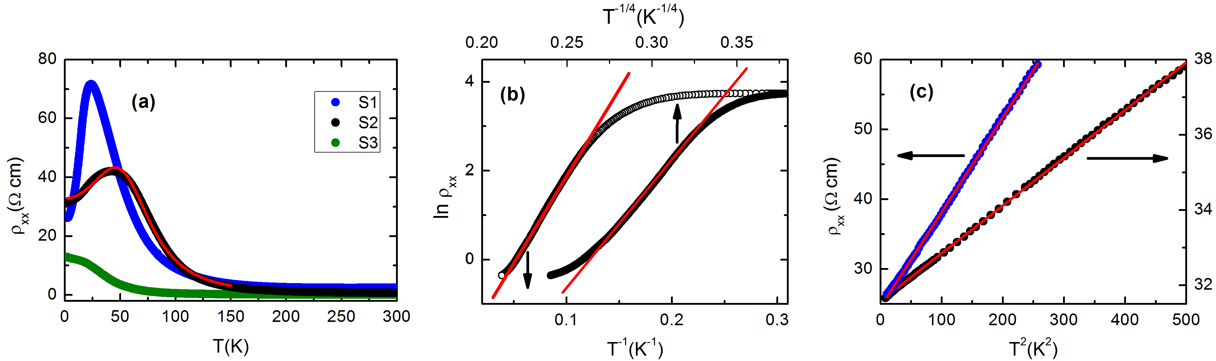
In order to understand the charge conduction mechanism, the temperature dependence of resistivity has been analysed. At high temperature, the insulating behavior of can be fitted with the Arrhenius equation . From the linear behavior of ln vs 1/ plot as shown in Fig. 1(b) for sample S2, we have deduced the value of activation energy, 40 meV. This value of activation energy is comparable to earlier reports Ren ; Pan ; Ko . However, in the low-temperature region, cannot be fitted with the activated type conduction. We have tried to fit the resistivity data with 3D Mott variable-range-hopping equation, , which has been shown in Fig. 1(b). In this case, a better fitting is obtained with K. The observed value of is quite large. () for S1 and S3 samples exhibits qualitative similar behaviour. Thus bulk conductivity shows activation behavior at high temperature but it switches over to 3D variable range hopping at low temperature. Crossover from activation to variable range hopping has also been reported earlier Ren ; Pan . In most of the cases, activation conductivity is observed in a narrow temperature range. In spite of much larger energy gap for some compositions, the bulk resistivity at low temperature is smaller than the present samples Pan . This is possibly due to the smaller value of (like the present S3 sample) which determines the bulk conductivity at low temperature.
For S1 and S2 crystals, the low-temperature resistivity below the peak, which is dominated by the surface state, shows an upward curvature, suggesting a superlinear temperature dependence of in the metallic region. We observe that below 21 K for sample S2 can be fitted well with the equation for =2. Figure 1(c) shows vs plot. It is clear from the figure that versus is strictly linear up to about 21 K. For crystal S1 also, exhibits dependence below 16 K. The dependence of resistivity at low temperature is the manifestation of Fermi liquid behavior of the surface carries. Electron-electron scattering is known to give rise a -dependent term in resistivity. The dependence of resistivity is observed in various strongly correlated electron systems such as heavy fermion metals, organic conductors and transition metal oxides. Though the behavior of resistivity is observed in several 3D Fermi liquid systems, it is rarely observed in 2D Fermi liquid systems. After creating a lateral magnetic superlattice, -dependent resistivity due to electron-electron Umklapp scattering has been observed in 2D electron gas at GaAs/AlGaAs heterointerface mess ; kato . The temperature dependence of relaxation time in electronic transport can differ from that of quasiparticle. Also, the relaxation time () of quasiparticle of a Fermi liquid system depends on the dimensionality. For example, in the 3D case whereas ln() in the 2D case, where is the Fermi energy uryu . However, the resistivity is proportional to in 3D as well as 2D systems uryu .
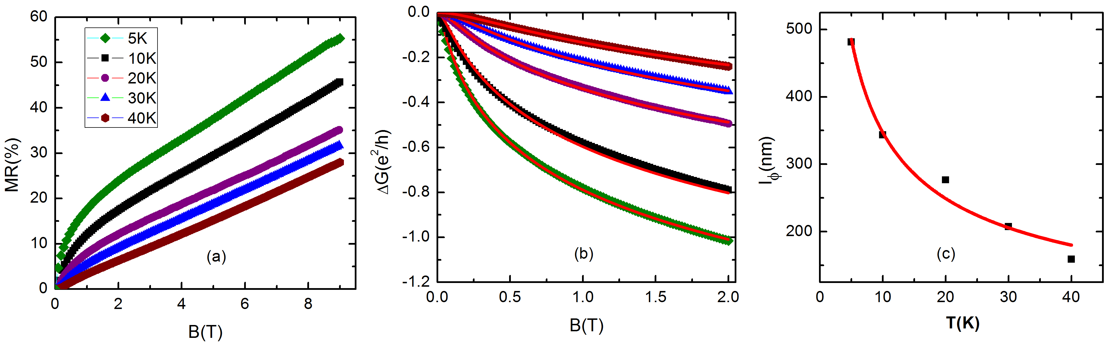
Magnetoresistance and weak anti-localization (WAL) effect in Bi1.5Sb0.5Te1.7Se1.3 single crystals. The magnetoresistance (MR) defined as [ has been measured in the field () range 0 to 9 T. The field dependence of MR at different temperatures is shown in Fig. 2(a) for the S2 sample as a representative. At low temperature, MR increases almost linearly in the high field region. The nonlinearity of MR at low fields is due to the weak anti-localization effect Lee ; Chen . With the application of magnetic field, the time reversal symmetry breaks down and a gap opens in the surface state. Hence, the rate of change of magnetoresistance, which is maximum in the limit 0, decreases with the increase in field strength. The well known Hikami-Larkin-Nagaoka (HLN) formula used to describe the WAL effect is given by hln ,
| (1) |
Here, the magneto-conductivity () is defined as =[() - (0)], is surface channel conductivity, the parameter represents the number of conduction channels (i.e., 0.5 for each conducting channel), and is the dephasing length. The WAL effect is solely a surface property and is the measure of its strength. The quadratic field dependence of magnetoresistance due to bulk is absent at low temperature. Thus, MR in the low temperature region originates from the conducting surface. The total electrical conductivity () of the single crystal is the sum of surface channel conductivity and bulk conductivity (), = + , where is the thickness of the sample. At low temperature, as the conductivity of bulk is very small compared to surface, is a good approximation. As is a tensor quantity in presence of magnetic field, has been calculated using the relation =/[+], where is the Hall resistivity. We have fitted the magneto-conductivity data with the HLN equation for fields below 2 T and shown in Fig. 2(b). The excellent fitting between experimental data and theoretical expression confirms that the low-temperature MR is due to the WAL effect. As shown in Fig. 2(c), reduces drastically with increasing temperature, following the theoretically predicted temperature dependence, alts ; lee1 ; lee2 ; choi . This observation further supports that the low-temperature transport is dominated by the surface state. We have also extracted the value of the parameter , which is 1 at 5 K and 10 K but it gradually decreases with increase in temperature and drops down to 0.8 at 40 K. The value of 1 implies that two conducting channels, top and bottom surfaces of the single crystal, are taking part in charge conduction at low temperature. At high temperatures, as significant fraction of the total current passes through the bulk, the value of decreases from 1.
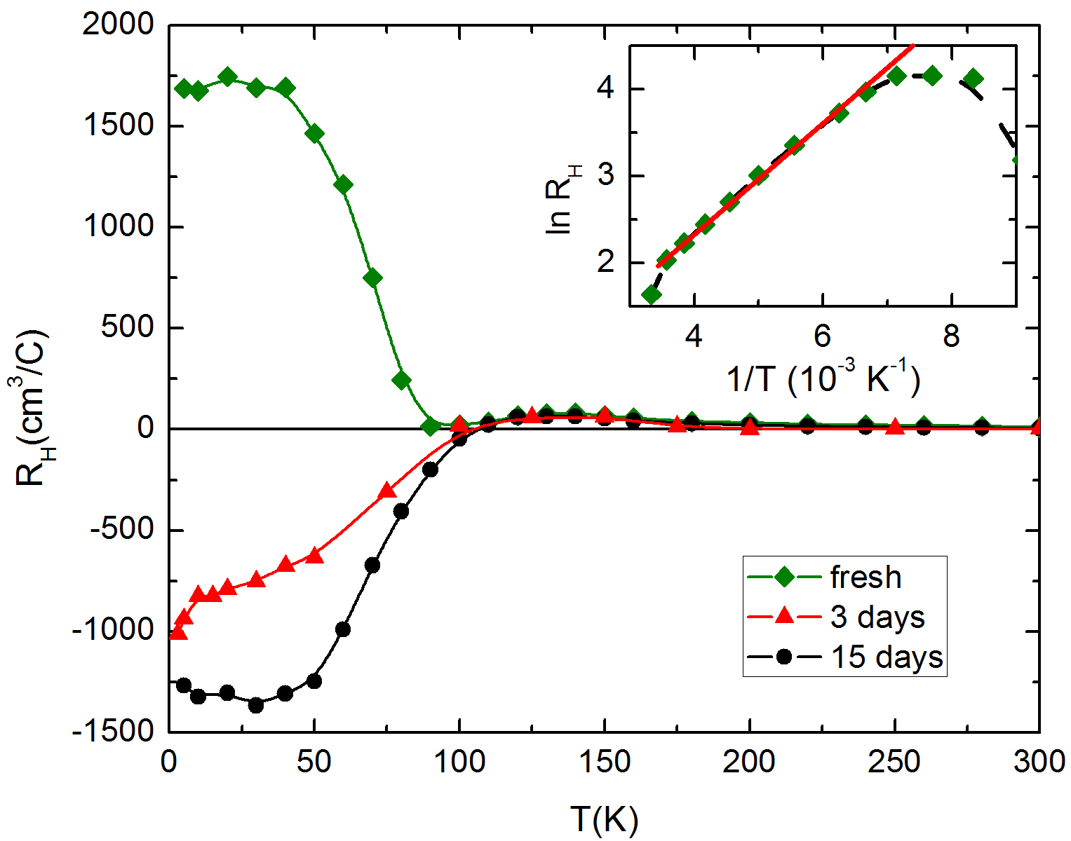
Hall resistivity and aging effect. The temperature dependence of the Hall coefficient () for several freshly prepared and aged crystals have been measured. For these crystals, is positive and shows activation behavior at high temperatures. The positive sign of implies that holes are the majority carriers at high temperatures. () for both freshly prepared and aged S2 crystals are shown in Fig. 3 as representative. As the Fermi level of BSTS lies in the gap of conduction band and valance band of the bulk, exhibits activation behavior Arakane . The value of activation energy deduced from the Hall data is about 39 meV which is very close to that calculated from resistivity. Valance band being closer to the Fermi level, -type carrier dominates the charge conduction in the bulk. The observed behavior of () in the range 125-300 K is qualitative similar to earlier reports on samples close to optimum composition Pan ; Ren ; Taskin . Though the surface dominance over the bulk is observed at much lower temperature (40 K) in , it starts at as high as 125 K for . In a two-band model, due to the high weightage of mobility than the density of carrier [7], the Hall response below 125 K is dominated by the high mobility carrier from the Dirac cone surface state. The freshly cleaved sample has -type surface state but the aged sample shows -type carrier as indicated by the sign of at low temperature. It has been observed that exposure to atmosphere causes electron doping on the surface, as a result, the Fermi level shifts above the Dirac point Taskin . This type of aging effect is quite common in topological insulator zhao . Thus the crystals those were exposed to air for longer time, starts to decrease sharply below 125 K and becomes negative at low temperature.
Singular paramagnetic response in magnetization measurements. Spin momentum locking is an integral characteristic of the surface state of a 3D topological insulator. As a result of strong spin-orbit coupling and time reversal symmetry, the spin and momentum wave vector of low-energy quasi particle excitations are always perpendicular to each other. This leads to left-handed spin texture for the conduction band and right-handed spin texture for the valence band on circular constant energy contour of the Dirac cones. However, at the Dirac node, where the two bands with opposite spin helicity touch each other, the spins are free to orient in any direction due to the singularity. As a consequence, it provides a paramagnetic contribution to the intrinsic magnetic moment of the system. Thus one expects to observe a low-field paramagnetic peak in the susceptibility curve (). Experimental discovery of this singular peak in has been reported for the family of 3D topological insulators and identified as the fingerprint of the helical spin texture of the Dirac fermions of the surface state zhao ; buga ; pariari . Also, shows linear-in-field decay from its zero-field value zhao ; buga ; pariari . The linear field dependence of has been established theoretically zhao . Considering =0, this paramagnetic Dirac susceptibility has the form,
| (2) |
at the sample’s native chemical potential ( = 0). Where , and are the Landé -factor, Bohr magneton and Fermi velocity respectively. is the effective size of the momentum space, which is responsible for the singular response in . As the height of the peak in is determined by , depending on the details of the bulk band, the peak height can vary from system to system within the family of 3D topological insulators zhao . Whereas the nature of the topological response determined by the cuspiness, the linear-in-field decay, robustness against temperature, etc. of () are universal to the entire family of 3D topological insulators zhao .
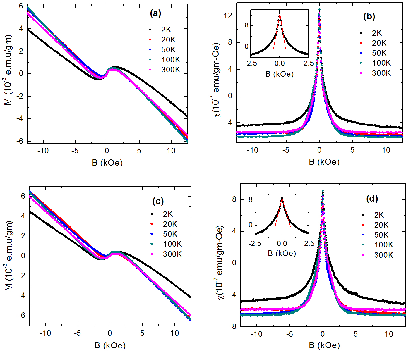
Figure 4(a) shows magnetization () of the freshly cleaved single crystal (S2) as a function of magnetic field, at several representative temperatures between 2 and 300 K. shows diamagnetic behaviour over a wide field range except at low fields, where a sharp paramagnetic upturn emerges. This is clearly visible from vs plot, as shown in Fig. 4(b). The experimental value of has been obtained after taking the first order derivative of with respect to . A cusp-like paramagnetic response in () sharply rises over the diamagnetic background in a narrow field range 1.5 kOe. Irrespective of temperature, the height of the peak from the diamagnetic background remains almost same. This singular response shows no sign of thermal rounding up to the highest measuring temperature 300 K. Similar to Bi2Se3, Sb2Te3, Bi2Te3 zhao ; buga and ZrTe5 pariari , the paramagnetic response in the present system implies the helical spin texture of the 2D Dirac fermion on the surface. In this context, we would like to mention that the standard diamagnetic sample such as Bi does not show any paramagnetic response in (see supplementary information). Inset of Fig. 4(b) shows linear decay of with field from its zero-field value at a representative temperature 2 K, as predicted theoretically (Eq. 2). When the surface is exposed to air for long time, the surface reconstruction and the formation of 2D electron gas occur due to the bending of bulk band zhao . As a result, the peak height has been observed to reduce with time zhao ; pariari . To probe the aging effect in BSTS, the magnetization measurements were done on the same piece of BSTS single crystal (S2) after 3 days of exposure to air and shown in Fig. 4(c). Although the nature of the peak along with the diamagnetic background, as shown in Fig. 4(d), remain unchanged, a significant drop ( 25%) is observed in the height, reflecting the expected aging effect in the present sample. Inset of Fig. 4(d) shows the linear decay of with field at 2 K for the aged sample.
Discussions
We observe a crossover from insulating to metallic behaviour in the temperature dependence of resistivity in Bi1.5Sb0.5Te1.7Se1.3 single crystals, which can be associated with the dominating bulk and surface state contribution to transport respectively. The competition between surface and bulk conduction appears to be very sensitive to sample preparation. A rare quadratic temperature dependent resistivity for metallic surface conduction has been observed for samples with large bulk resistivity. This highly decoupled metallic surface, which was remained elusive in earlier studies, is an essential criterion for the use of spin-momentum locked topological state in electronic application and basic research. In addition, we observe a sharp cusp-like paramagnetic peak at zero field in magnetization measurements. This temperature insensitive anomalous magnetic response, has been associated with the helical spin texture of 2D Dirac fermion on the surface of 3D topological insulators. The surface state reconstruction with time due to doping from air, known as aging effect for 3D topological insulators, is clearly reflected from the age dependent reduction of the susceptibility peak.
Method
Single crystals of Bi1.5Sb0.5Te1.7Se1.3 were prepared by self-flux method using high purity elements (5N) of Bi, Sb, Te and Se in a stoichiometric ratio 1.5:0.5:1.7:1.3, respectively. Two slightly different techniques were adopted to prepare these crystals. In both the cases sample handling was done inside a glove box in argon gas atmosphere. Method I: Single crystal S3 was prepared in this method. Stoichiometric mixture of Bi, Sb, Te and Se granules was vacuumed sealed in a quartz tube and then heated at the rate of 70∘C/h to 850 ∘C and kept at that temperature for 48 h for diffusion process. The sample was cooled over a period of 60 h to 550 ∘C and kept at that temperature for 96 h before furnace cooling. Method II: Some minor modifications were done over method I to prepare single crystals S1 and S2. The stoichiometric mixture of elements was pelletised before the vacuum sealing. In this method, at the final stage (of method I) the sample was slowly cooled from 550 ∘C to room temperature at the rate of 10∘/h instead of furnace cooling. The local temperature gradient, which sustains due to the slow cooling process, in the vertically placed tube helps in stacking of chalcogenite layer and growing large single crystalline flake which can be easily cleaved using a razor. The typical thickness of the samples used in electrical transport and magnetic measurements is 100 m. In-plane electrical resistivity and Hall coefficient between 2 and 300 K were measured by four-probe technique in a physical property measurement system (Quantum Design). Magnetization measurement was performed in SQUID-VSM (Quantum Design). Before magnetization measurement of BSTS, the system was counterchecked by standard bismuth and palladium samples, the details of which are discussed in the supplementary along with sample characterization.
References
-
(1)
Heish, D. et al. A topological Dirac insulator in a quantum spin Hall phase. Nature 452, 970-974 ( 2008).
-
(2)
Xia, Y. et al. Observation of a large-gap topological-insulator class with a single Dirac cone on the surface. Nature Physics 5, 398-402 (2009).
-
(3)
Heish, D. et al. Observation of Time-Reversal-Protected Single-Dirac-Cone Topological-Insulator States in Bi2Te3 and Sb2Te3. Physical Review Letter 103, 146401(2009).
-
(4)
Hasan, M. Z. & Kane, C. L. Colloquium: Topological insulators. Reviews of Modern Physics 82, 3045 3067 (2010).
-
(5)
Qi, X.-L. & Zhang, S.-C. Topological insulators and superconductors. Reviews of Modern Physics 83, 1057 1110 (2011).
-
(6)
Eto, K., Ren, Z., Taskin, A.A.,Segawa, K.,& Ando, Y. Angular-dependent oscillations of the magnetoresistance in Bi2Se3 due to the three-dimensional bulk Fermi surface. Physical Review B. 81, 195309 (2010).
-
(7)
Qu,D-X., Hor, Y.S., Xiong, J., Cava,R.J., & Ong, N.P. Quantum Oscillations and Hall Anomaly of Surface States in the Topological Insulator Bi2Te3. Science 329, 821 (2010).
-
(8)
Dutta, P., Bhoi, D., Midya, A., Khan, N., & Mandal, P. Anomalous thermal expansion of Sb2Te3 topological insulator. Applied Physics Letter 100, 251912 (2012).
-
(9)
Hor, Y. S.et al. p-type Bi2Se3 for topological insulator and low-temperature thermoelectric applications. Physical Review B 79, 195208 (2009).
-
(10)
Taskin, A. A., Ren, Z., Sasaki, S., Segawa, K., & Ando, Y. Observation of Dirac Holes and Electrons in a Topological Insulator. Physical Review Letter 107, 016801 (2011).
-
(11)
Ren, Z., Taskin, A. A., Sasaki, S., Segawa K. & Ando, Y. Optimizing Bi2-xSbxTe3-ySey solid solutions to approach the intrinsic topological insulator regime. Physical Review B. 84. 165311 (2011).
-
(12)
Shekhar, C. et al. Evidence of surface transport and weak antilocalization in a single crystal of the Bi2Te3Se topological insulator. Physical Review B 90, 165140 (2014).
-
(13)
Teramoto, I. & Takayanagi, S. Relations between the electronic properties and the chemical bonding of SbxBi2-xTe3-ySey system. Journal of Physics and Chemistry of Solids 19, 124 (1961).
-
(14)
Hsiung, T. -C. et al. Enhanced surface mobility and quantum oscillations in topological insulator Bi1.5Sb0.5Te1.7Se1.3 nanoflakes. Applied Physics Letter103, 163111 (2013).
-
(15)
Pan, Y. et al. Low carrier concentration crystals of the topological insulator Bi2-xSbxTe3-ySey: a magnetotransport study. New Journal Physics 16 123035 (2014).
-
(16)
Segawa, K., Ren, Z., Sasaki, S., Tsuda T., Kuwabata, S., & Ando, Y. Ambipolar transport in bulk crystals of a topological insulator by gating with ionic liquid. Physical Review B 86, 075306 (2012).
-
(17)
Lee, J., Park, J., Lee, J-H., Kim, J. S. & Lee, H. -J. Gate-tuned differentiation of surface-conducting states in Bi1.5Sb0.5Te1.7Se1.3
topological-insulator thin crystals. Physical Review B 86, 245321 (2012).
-
(18)
Frantzeskakis, E. et al. Dirac states with knobs on: Interplay of external parameters and the surface electronic properties of three-dimensional topological insulators. Physical Review B 91, 205134 (2015).
-
(19)
Ko, W. et al. Atomic and electronic structure of an alloyed topological insulator Bi1.5Sb0.5Te1.7Se1.3. Science Reports 3, 2656 (2013).
-
(20)
Post, K. W. et. al. Infrared probe of the bulk insulating response in Bi2-xSbxTe3-ySey topological insulator alloys. Physical Review B 91, 165202 (2015)
-
(21)
Kim, S. et al. Robust Protection from Backscattering in the Topological Insulator Bi1.5Sb0.5Te1.7Se1.3. Physical Review Letter 112, 136802 (2014).
-
(22)
Arakane, T. et al. Tunable Dirac cone in the topological insulator Bi2-xSbxTe3-ySey. Nature Communications 1639 3:636 (2012).
-
(23)
Messica, A. et al. Suppression of Conductance in Surface Superlattices by Temperature and Electric Field. Physical Review Letter 78, 705 (1997).
-
(24)
Kato, M., Endo, A., Katsumoto, S. & Iye, Y. Two-dimensional electron gas under a spatially modulated magnetic field: A test ground for electron-electron scattering in a controlled environment. Physical Review B 58, 4876 (1998).
-
(25)
Uryu, S. & Ando, T. Umklapp electron-electron scattering in weakly modulated two-dimensional electron systems. Physical Review B 64, 195334 (2001).
-
(26)
Chen, J. et al. Gate-Voltage Control of Chemical Potential and Weak Antilocalization in Bi2Se3. Physical Review Letter 105, 176602 (2010).
-
(27)
Hikami, S., Larkin, A. I., & Nagaoka, Y. Spin-Orbit Interaction and Magnetoresistance in the Two Dimensional Random System. Progress of Theoretical Physics 63 707 (1980).
-
(28)
Altshuler, B. L., Aronov, A. G., & Khmelnitsky, D. E. Effects of electron-electron collisions with small energy transfers on quantum localisation. J. Phys. C 15, 7367 (1982).
-
(29)
Lee, P. A. & Stone, A. D. Universal Conductance Fluctuations in Metals. Physical Review Letter 55, 1622 (1985).
-
(30)
Lee, P. A., Stone, A. D. & Fukuyama, H. Universal conductance fluctuations in metals: Effects of finite temperature, interactions, and magnetic field. Physical Review B 35, 1039 (1987).
-
(31)
Choi, K. K., Tsui,D. C., & K. Alavi, K. Dephasing time and one-dimensional localization of two-dimensional electrons in GaAs/AlxGa1-xAs heterostructures. Physical Review B 36, 7751 (1987).
-
(32)
Zhao, L. et al. Singular robust room-temperature spin response from topological Dirac fermions. Nature Material13, 580 (2014).
-
(33)
Buga, S. G. et. al. Superconductivity in bulk polycrystalline metastable phases of Sb2Te3 and Bi2Te3 quenched after high-pressure high-temperature treatment. Chemical Physics Letter 631-632, 97 (2015).
-
(34)
Pariari, A., & Mandal, P. Coexistence of topological Dirac fermions in the surface and three-dimensional Dirac cone state in the bulk of ZrTe5 single crystal. arXiv:1603.05175.
Supplementary information for “Prominent metallic surface conduction and the singular magnetic response of topological Dirac fermion in three-dimensional topological insulator Bi1.5Sb0.5Te1.7Se1.3”
.1 Sample characterization using powder x-ray diffraction and energy dispersive x-ray techniques
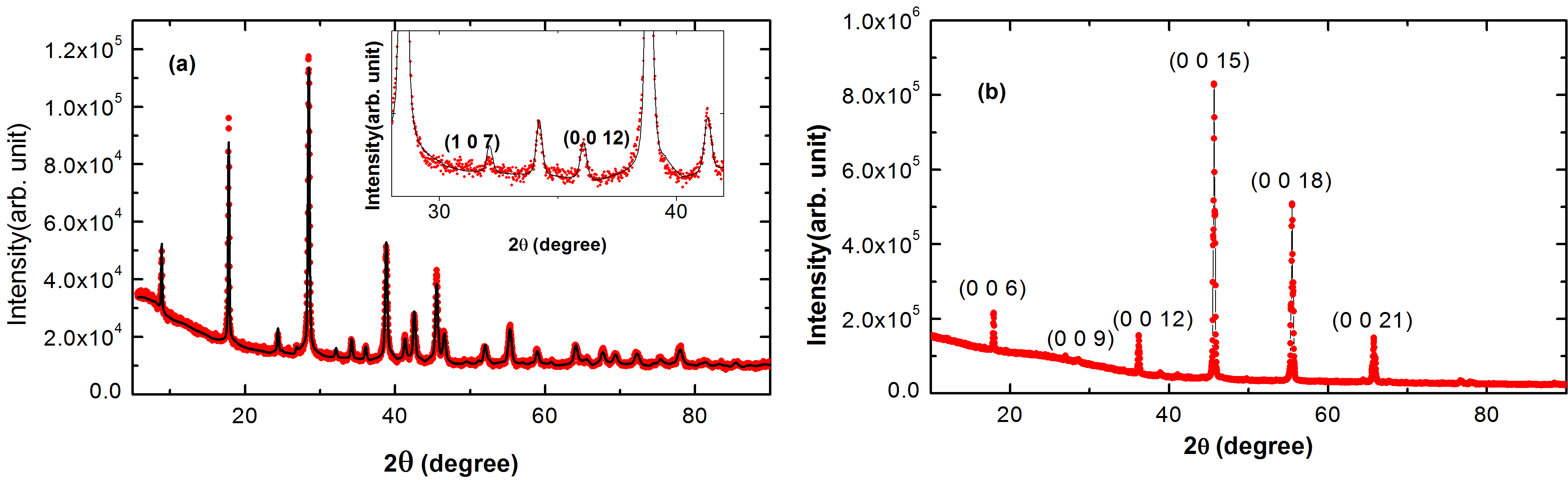
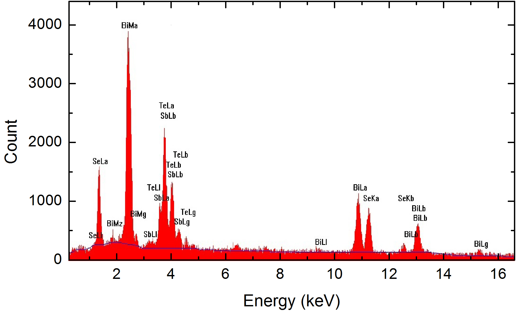
The phase purity of Bi1.5Sb0.5Te1.7Se1.3 (BSTS) samples was checked by high resolution powder x-ray diffraction (XRD) method with Cu Kα radiation in a Rigaku x-ray diffractometer (TTRAX II). Within the resolution of XRD, we have not observe any peak due to impurity phase. Fig. S5(a) shows the diffraction pattern for powdered crystal prepared by method II as a representative. The diffraction profile can be fitted well with hexagonal structure of space group symmetry Rm using the Rietveld refinement. The calculated lattice parameters are =4.2840 Å and =29.871 Å. Inset of Fig.S5(a) shows (1 0 7) and (0 0 12) peaks. The presence of these peaks are very important for ordering of chalcogen layer. We have also performed x-ray diffraction of a single flake as shown in Fig.S5(b). The Bragg peaks, which are integer multiple of (003) only are observed, indicating good -axis orientation of the single crystal. The (0 0 12) peak is also very clearly observed in the diffraction pattern. Energy dispersive x-ray (EDX) (Quanta 200, FEG scanning electron microscope) analysis was used to determine the chemical composition of the sample. Identical chemical composition at different positions of single flake and for different flakes suggest that the samples are chemically homogeneous. Fig.S6 shows the typical EDX spectrum of one such BSTS single crystal. The chemical composition determined using EDX is close that of nominal composition, at least within the limits of the SEM-EDX analysis.
.2 Magnetic measurements of standard samples
We have measured field response of magnetic moment of standard bismuth and palladium samples in SQUID-VSM [MPMS 3, Quantum Design] prior to BSTS single crystal. FIG.S7 (a) shows that linear diamagnetic moment of bismuth at 2 and 100 K passes through the origin. This is more clear from FIG.S7 (b), which shows magnetic field dependence of differential susceptibility (=). Absence of any paramagnetic peak around zero field implies that singular paramagnetic susceptibility in BSTS single crystal is not due to any spurious response in our system.
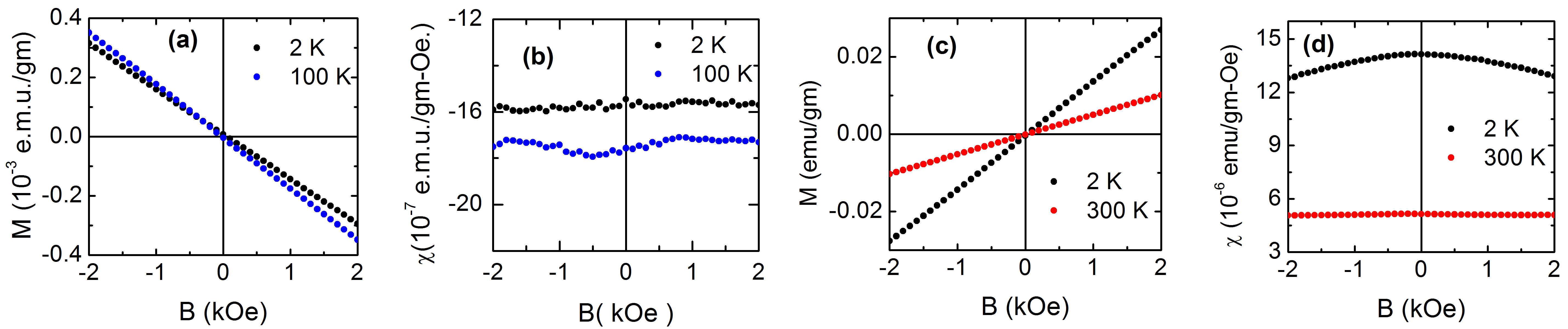
FIG. S7(c) shows the expected magnetic behaviour of paramagnetic palladium sample, provided by Quantum Design. FIG.S7(d) shows the low-field susceptibility of palladium at 2 K and room temperature. The nonlinear behaviour of at low field and a broad zero field peak at 2 K are completely suppressed with increasing temperature. This behavior is entirely different from the singular, robust and linear low-field paramagnetic response of the topological surface state in the present sample.
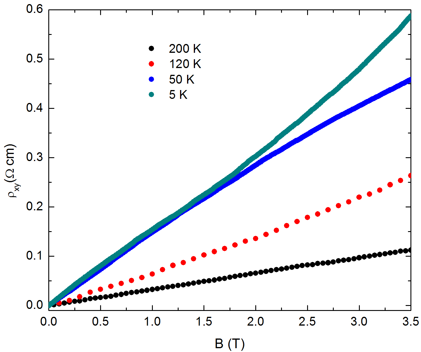
.3 Field dependence of the Hall resistivity
The field dependence of Hall resistivity () of freshly cleaved BSTS is plotted in Fig.S8 at some representative temperatures from 5 to 200 K. The slope of the vs plot at low field, provides the value of Hall coefficient (RH) at that temperature as discussed in the manuscript. is positive and increases almost linearly with field from room temperature to 120 K. This behavior of RH indicates that -type charge carrier dominates the conductivity of the bulk at high temperature. As the temperature decreases further, nonlinearity in vs starts to appear because the surface contribution becomes significant due to exponential decrease in bulk carrier. Thus, due to presence of two different bands with different carrier concentration and mobility, the field dependence of becomes nonlinear, as shown in Fig.S8 at 5 and 50 K. Although is weakly nonlinear at high fields, the low-field values of RH is almost same at low temperatures.