Mass inversion in graphene by proximity to dichalcogenide monolayer
Abstract
Proximity effects resulting from depositing a graphene layer on a TMD substrate layer change the dynamics of the electronic states in graphene, inducing spin orbit coupling (SOC) and staggered potential effects. An effective Hamiltonian that describes different symmetry breaking terms in graphene, while preserving time reversal invariance, shows that an inverted mass band gap regime is possible. The competition of different perturbation terms causes a transition from an inverted mass phase to a staggered gap in the bilayer heterostructure, as seen in its phase diagram. A tight-binding calculation of the bilayer validates the effective model parameters. A relative gate voltage between the layers may produce such phase transition in experimentally accessible systems. The phases are characterized in terms of Berry curvature and valley Chern numbers, demonstrating that the system may exhibit quantum spin Hall and valley Hall effects.
Graphene has many interesting properties intensively studied in recent years Castro Neto et al. (2009). Prominent among these, possible intrinsic spin orbit coupling (SOC) on its charge carriers was estimated by Kane and Mele to be rather weak, Kane and Mele (2005). Improved estimates that include contributions from -orbitals yield larger values, 24 Gmitra et al. (2009), although still rather weak for experimental observation. Several ways have been proposed to enhance the spin orbit interaction in graphene for uses in spintronics Pesin and MacDonald (2012). Enhancing hybridization by adding hydrogen or fluorene atoms Avsar et al. (2015), as well as decorating with heavy adatoms Weeks et al. (2011), or different substrates Giovannetti et al. (2015), have been proposed to produce large SOC. Depositing graphene on metallic substrates has also resulted in strong SOC for the charge carriers in graphene Marchenko et al. (2012).
The availability of 2D crystals allows for novel stacked heterostructures with strong proximity effects. Electronic modulation due to such substrates has been studied in graphene, such as hBN or twisting of another graphene layer Bistritzer and MacDonald (2011); Xue et al. (2011); Moon and Koshino (2014); McCann and Koshino (2013); Ren et al. (2015); Gorbachev et al. (2014). Lattice commensurability in these heterostructures depends on factors such as isotropic expansion, relative sliding between layers, and relative twists Hermann (2012); Moon and Koshino (2014); Zhang et al. (2014).
An interesting family of 2D crystals, transition metal dichalcogenides (TMD) can be used as substrates for graphene Geim and Grigorieva (2013); Jiang (2015); Gmitra et al. (2016); Wang et al. (2015); Gmitra and Fabian (2015). Monolayer semiconductor TMD such as MoS2 and WS2 have a direct band gap and honeycomb crystal structure Xiao et al. (2012). The bands near the Fermi energy are formed predominantly from , and orbitals of the metal atom Liu et al. (2013), with slight admixture from the -orbitals of the chalcogen. The SOC in the valence bands is much larger than in the conduction bands, with strength that varies with the transition metal Rose et al. (2013). Successful growth of graphene on MoS2 and WS2 has been demonstrated experimentally Lu et al. (2014); Wang et al. (2015); Avsar et al. (2014). First principles calculations on some of these systems have proved challenging Gmitra et al. (2016); Wang et al. (2015); Gmitra and Fabian (2015), with reported results that differ qualitatively and quantitatively.
Motivated by these works, we study the topological properties of the minimal time reversal invariant effective model of graphene that incorporates geometrical and orbital perturbation effects expected in these systems. We focus on the Berry curvature and associated valley Chern number and identify different quantum phases that may appear as Hamiltonian parameters vary. The phase diagram shows that under the right conditions, it is possible to achieve band inversion of spin-split bands in graphene that acquire interesting characteristics from the proximal TMD layer. We further identify that a relative voltage difference between the graphene and TMD layer (as obtained by an applied external field) can derive a transition between two topologically inequivalent phases, separated by a semimetallic phase.
The reduction of the spatial symmetries of graphene, and the enhancement of SOC in these systems results in the generation of spin resolved gaps at the Dirac point. The interplay between sublattice symmetry breaking and enhanced SOC parameters determines the size and topological nature of the gaps in the system. As the gaps are dominated by the SOC, the system becomes a quantum spin Hall insulator, with symmetry protected edge states. In contrast, when the gaps are dominated by the sublattice staggered symmetry, the system becomes a valley Hall insulator.
Identification of experimentally relevant parameters is carried out utilizing a tight binding formalism with appropriate graphene and TMD characteristics. Different lattice orientations and relative layer displacement are also found to exhibit such phase transition, with shifts in the values of external field at which it occurs.
Effective model and characteristics.
The proximity of the TMD monolayer to graphene breaks inversion symmetry, which allows for the presence of Rashba SOC, in addition to sublattice asymmetry terms in the effective Hamiltonian at low energies Asmar and Ulloa (2014). A minimal low energy model will include terms that respect time reversal symmetry Gmitra and Fabian (2015); Asmar and Ulloa (2015), and arise due to the symmetries in the TMD states, , with
| (1) |
where , , and are Pauli matrices with , (where 0 is used for the unit matrix) operating on different degrees of freedom. acts on the pseudospin sublattice space (A,B), on the K, K′ valley space, and on the spin degree of freedom Asmar and Ulloa (2014). We use the ‘standard’ basis , with , and describes pristine graphene at low energy Kane and Mele (2005). The parameters , and are constants of the model, to be obtained from DFT or tight-binding calculations (as we describe below). They would naturally be expected to depend on the microscopic details of the system, such as orientation and relative displacements of the monolayers, as well as on applied electric fields. As we will see below, it is such dependence that may give rise to interesting phases.
Different terms in the effective model play interesting physical roles. characterizes the (staggered) sublattice asymmetry in the graphene A and B atoms, as one expects from the proximity to the TMD monolayer; this term is well-known to open gaps in the otherwise linear dispersion of , and create sizable topological-valley currents in graphene-hBN superlattices Gorbachev et al. (2014); Asmar and Ulloa (2015). The intrinsic SOC term, , opens a spin gap in the bulk structure with opposite signs at the K and K′ valleys, while preserving spatial symmetries of the hexagonal lattice. Finally, as mirror symmetry () is broken in the presence of the TMD substrate, the dynamics is expected to contain a Rashba effective Hamiltonian Kane and Mele (2005), and a diagonal SOC term . Although a valley mixing term is possible in principle, we find it to be essentially null in all our calculations.
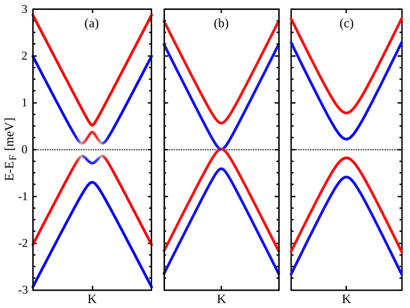
Typical band structures for this Hamiltonian are shown in Fig. 1. The left panel illustrates an ‘inverted band’ regime, evident in the local dispersion around each of the valleys near the graphene neutrality point, produced by the anticrossing of bands with opposite spins and due to the presence of the Rashba term. The middle panel shows a transition point, where the gap has closed and exhibits a dispersion with nearly full spin polarization. The right panel shows a ‘direct band’ regime with a simple parabolic dispersion for each of the two spin projections. As we will see below, the inverted band regime is achieved whenever , while the direct band regime is achieved in the opposite case.
One can analyze the topological features of the states described by the effective Hamiltonian (1) by calculating the Berry curvature and Chern number per valley of the occupied bands using Xiao et al. (2010)
| (2) |
where is the band number, and is the velocity operator along the direction Qiao et al. (2013). Figure 2 shows Berry curvature for the two lowest energy (valence) bands, and total curvature near each of the K and K′ valleys, in two different parameter regimes. Notice plots for each band obey (K-valley(K′-valley), as required by time reversal symmetry Xiao et al. (2010). The left two columns in Fig. 2, for the inverted band regime, exhibit a non-monotonic -dependence for the curvature in each valley, with inversion at each K point, , so that the total valley curvature is nearly null. In contrast, the right two columns for the direct band regime show the same curvature for both bands in each valley. The non-vanishing Berry curvature in each valley may give rise to interesting edge states in systems with borders, as seen in graphene ribbons and TMD flake edges Hao et al. (2008); Li et al. (2011); Segarra et al. (2016).

The total Chern index at each valley yields for all parameter values, so that the overall Chern number vanishes, as expected for systems protected by time reversal symmetry Qiao et al. (2012); Xiao et al. (2010). However, the spin splitting and mixing of the two valence bands in different regimes results in , with an overall sign change across the semimetallic phase transition where the gap closes. In a system with zero Rashba term (), the Chern number can be shown to yield , indicating the competition between the intrinsic SOC and staggered perturbations. Although an analytic expression for the Chern number is not feasible in general, numerical evaluation for different parameter regimes reveals the important roles of both and , as well as , on determining the topological features of the system. We will return to this below in detail.
Tight binding model.
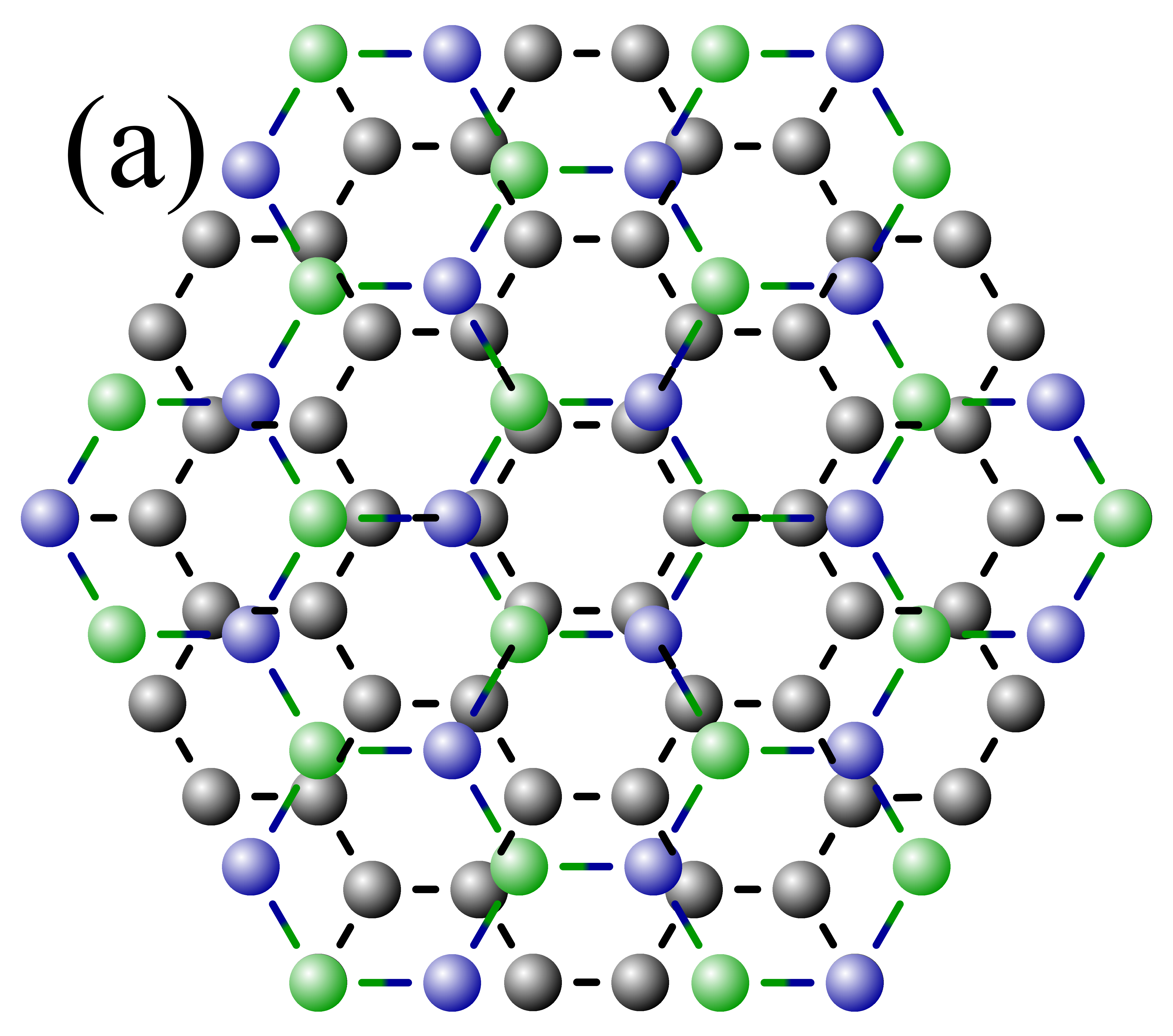
To study the relevant effective model dependence on microscopic details of the graphene-TMD heterostructure, we have implemented a tight-binding model of the structure. For specificity, we focus on graphene and MoS2, with lattice constants 2.46 and 3.11 , respectively. A superlattice of 55 graphene unit cells and 44 MoS2 results in a nearly commensurate moire pattern with a small residual strain (1.1 ), as seen in Fig. 3a.
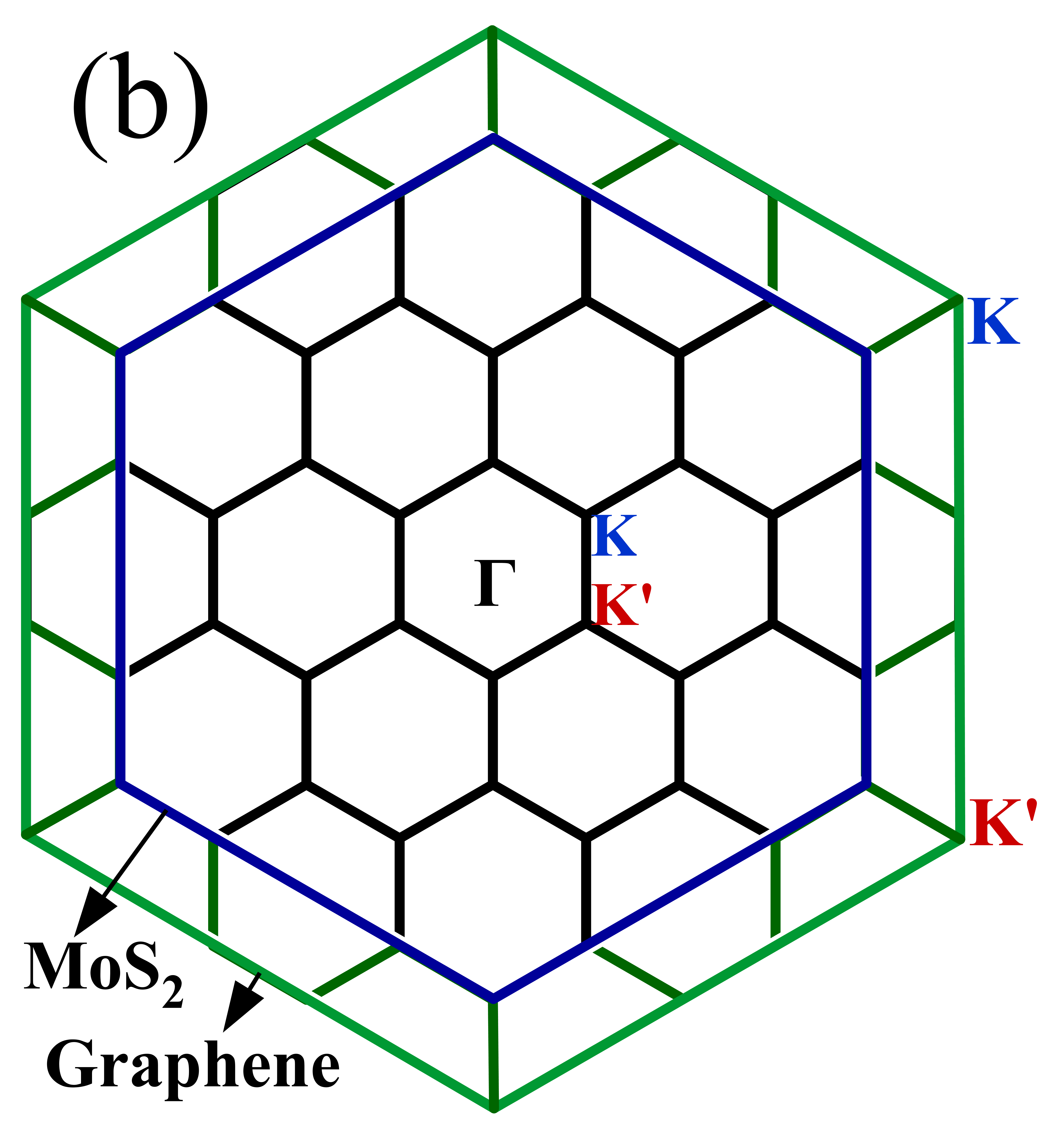
The primitive lattice vectors in such superlattice are connected by a linear transformation Hermann (2012), , where are the primitive vectors in each layer ( = graphene and MoS2). The superlattice has primitive lattice vectors given by ; here . The reduced Brillouin zone has similar features to that of graphene, with valleys at , , , which fold the corresponding valleys of graphene and MoS2 onto the same points; see Fig. 3b.
The tight-binding formalism couples nearest neighbors in an optimal basis where MoS2 is represented by three orbitals, , and Liu et al. (2013),
| (3) |
considers the on-site energies of Mo-atom , orbital , and spin , while describes nearest neighbor hopping between Mo orbitals. The SOC in MoS2 is introduced via atomic contributions Liu et al. (2013). For graphene we adopt the usual -orbital representation with two-atom basis Castro Neto et al. (2009); Sup . The substrate generates an electric field normal to the layer, causing a Rashba SOC term Kane and Mele (2005), , where describe spin up and down states, and is the unit vector that connects neighbor atoms A and B. Although the Rashba interaction is weak in graphene (meV Konschuh et al. (2010)), it is an important term that breaks inversion symmetry.
The interlayer coupling between graphene orbital and MoS2 -orbitals is given by
| (4) |
We take coupling to nearest neighbors across layers, where is parameterized by the distance connecting atoms in both layers, , normalized to a constant ; describes the coupling between and -orbitals using a Slater-Koster approach Slater and Koster (1954). The couplings depend naturally on the orbitals involved, which results in being larger than and , due to a higher overlap. The parameters used are described in the supplement Sup , although the detailed values do not affect the main conclusions nor qualitative behavior, providing only an overall scaling of parameter ranges.
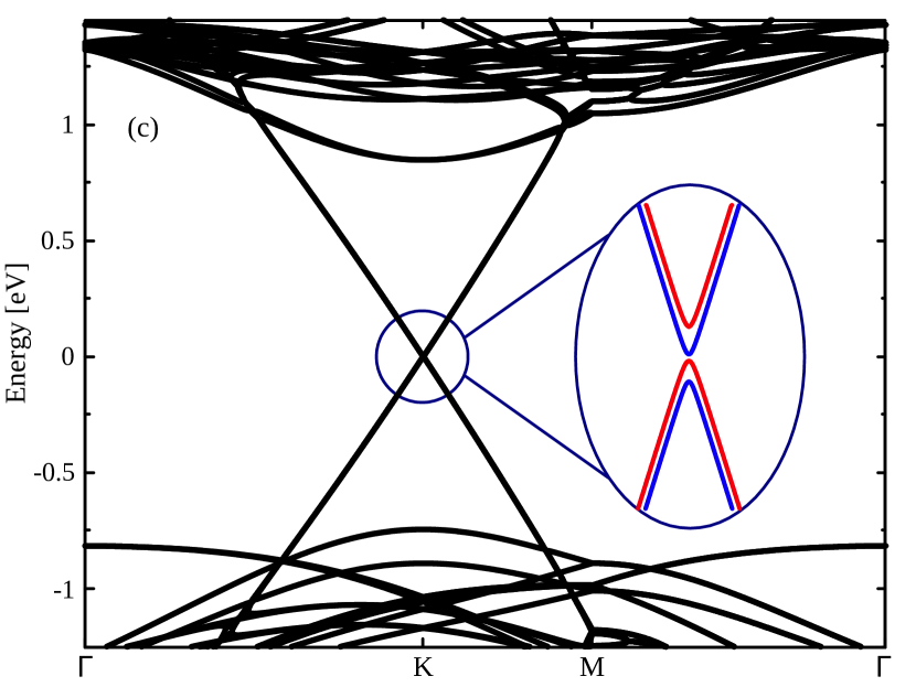
The tight-binding model considers the possibility of a difference in electronegativity between the two layered materials creating a relative shift of their neutrality points. This polarization shift could further be thought to arise from an applied voltage between the layers, as it would be possible (in principle) to apply if the graphene-MoS2 structure is placed between capacitor plates. We explore the consequences of such relative voltage on the effective band structure on graphene, assuming that the other parameters (hopping integrals and lattice constants) remain unchanged with voltage. One could obtain the appropriate parameters from first principles calculations, although the van der Waals nature of the bonding between layers, as well as the rather fine-scale of the relevant features make those calculations quite challenging Wang et al. (2015); Gmitra et al. (2016). Results for a nearly zero relative shift of the neutrality points are in Fig. 3c, which show how the low energy spectrum exhibits a finite gap for fully spin polarized bands.
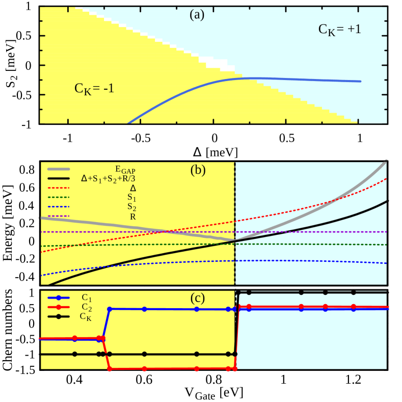
As the relative voltage between layers is varied, the tight-binding spectrum shows a low-energy band structure similar to that of the effective model, Fig. 1. We have carried out a systematic fit of the low energy dispersion with the model parameters in Eq. 1, as the voltage changes. The fits are excellent (to less than one percent) up to an energy 0.3 eV away from the graphene Dirac point. The effective model describes not only the low-energy band dispersion, but also the full spin and pseudospin structure of the states, illustrating the generality of the model Sup . Fit parameters vary smoothly with gate voltage, as shown in Fig. 4b; we assign when graphene Dirac point is 20 meV higher than the top valence band in MoS2, while a zero relative shift of their neutrality points is at . The staggered potential increases smoothly with voltage, while , , and vary much less 111We have kept constant in the tight binding calculations, although a gate voltage dependence is likely. This would be expected to reduce the gate voltage required to close the gap.. Most importantly, we see that the gap closes near the gate voltage where the sum . Figure 4a and b also show the valley Chern number jumps by at the closing of the gap, as anticipated from the discussion above, although here the competition involves and all three SOC coefficients. We emphasize that the closing of the gap and corresponding phase transition from an inverted mass to a direct gap regime is rather generic, and as suggested by these calculations, accessible experimentally.
It is important to notice that the model studied is one particular example of a large class of Hamiltonians that describe systems that possess similar symmetry properties with different parameters. More examples are graphene and other TMD heterostructures, with some quantitative differences. In graphene-WS2, the inverted band phase exists over a wider range of gate voltage, with gap closing at eV. This larger voltage can be understood as arising from the larger SOC in WS2, nearly three times stronger than in MoS2 Xiao et al. (2012). We also explored structures with a relative shift of the lattices, or possible rotations of the two layers involved. We find that gaps open generically near the graphene neutrality point, with regimes of inverted masses, at times over only narrow regions of gate voltage. This suggests that in a macroscopic sample with a distribution of strains, one may expect variation of the effective Hamiltonian parameters over long range scales. This may produce ‘edge states’ separating different regions in the 2D bulk with different topological features, resulting interesting effects even away from the sample edges.
The topology of the inverted mass regime in the structure suggests that interesting edge states would exist at boundaries, as discussed in the past Xiao et al. (2010). In fact, zigzag edge graphene nanoribbons based on the effective Hamiltonian show different regimes. A quantum spin Hall effect is seen for the mass inverted bands, while a valley Hall effect is present in the direct band regime.
Conclusions.
We have built and studied a heterostructure of graphene deposited on a monolayer of transition metal dichalcogenides (TMD) in order to explore proximity effects. An effective Hamiltonian with possible perturbations that preserve time reversal is able to faithfully reproduce the results from tight binding calculations of the structure near the graphene Dirac points. The proximity of the TMD results in sizable spin orbit coupling imparted onto graphene, in a degree proportional to the intrinsic SOC in the TMD. This strong effect is found to compete with the staggered potential also introduced, resulting in different regimes where the heterostructure changes phase from an inverted mass band structure, with possible quantum spin Hall effect and the consequent spin filtered edge states, to a direct band structure with possible valley Hall effect and the appearance of valley currents. These phases could in principle be controlled by a relative gate voltage between the layers, and may even be present throughout the 2D bulk, as strains fields would affect the relevant phases present.
Acknowledgments. We acknowledge support from NSF-DMR 1508325, the Saudi Arabian Cultural Mission to the US for a Graduate Scholarship, and hospitality of the Aspen Center for Physics, supported by NSF-PHY 1066293.
References
- Castro Neto et al. (2009) A. H. Castro Neto, F. Guinea, N. M. R. Peres, K. S. Novoselov, and A. K. Geim, Rev. Mod. Phys. 81, 109 (2009).
- Kane and Mele (2005) C. L. Kane and E. J. Mele, Phys. Rev. Lett. 95, 226801 (2005).
- Gmitra et al. (2009) M. Gmitra, S. Konschuh, C. Ertler, C. Ambrosch-Draxl, and J. Fabian, Phys. Rev. B 80, 235431 (2009).
- Pesin and MacDonald (2012) D. Pesin and A. H. MacDonald, Nature Materials 11, 409 (2012).
- Avsar et al. (2015) A. Avsar, J. H. Lee, G. K. W. Koon, and B. Ö zyilmaz, 2D Materials 2, 044009 (2015).
- Weeks et al. (2011) C. Weeks, J. Hu, J. Alicea, M. Franz, and R. Wu, Phys. Rev. X 1, 021001 (2011).
- Giovannetti et al. (2015) G. Giovannetti, M. Capone, J. van den Brink, and C. Ortix, Phys. Rev. B 91, 121417 (2015).
- Marchenko et al. (2012) D. Marchenko, A. Varykhalov, M. Scholz, G. Bihlmayer, E. Rashba, A. Rybkin, A. Shikin, and O. Rader, Nat. Commun. 3, 1232 (2012).
- Bistritzer and MacDonald (2011) R. Bistritzer and A. H. MacDonald, Proceedings of the National Academy of Sciences 108, 12233 (2011).
- Xue et al. (2011) J. Xue, J. Sanchez-Yamagishi, D. Bulmash, P. Jacquod, A. Deshpande, K. Watanabe, T. Taniguchi, P. Jarillo-Herrero, and B. J. LeRoy, Nature Materials 10, 282 (2011).
- Moon and Koshino (2014) P. Moon and M. Koshino, Phys. Rev. B 90, 155406 (2014).
- McCann and Koshino (2013) E. McCann and M. Koshino, Reports on Progress in Physics 76, 056503 (2013).
- Ren et al. (2015) Y. Ren, X. Deng, Z. Qiao, C. Li, J. Jung, C. Zeng, Z. Zhang, and Q. Niu, Phys. Rev. B 91, 245415 (2015).
- Gorbachev et al. (2014) R. Gorbachev, J. Song, G. Yu, A. Kretinin, F. Withers, Y. Cao, A. Mishchenko, I. Grigorieva, K. Novoselov, L. Levitov, and A. K. Geim, Science 346, 448 (2014).
- Hermann (2012) K. Hermann, J. Phys.: Cond. Mat. 24, 314210 (2012).
- Zhang et al. (2014) J. Zhang, C. Triola, and E. Rossi, Phys. Rev. Lett. 112, 096802 (2014).
- Geim and Grigorieva (2013) A. K. Geim and I. V. Grigorieva, Nature 499, 419 (2013).
- Jiang (2015) J.-W. Jiang, Frontiers of Physics 10, 287 (2015).
- Gmitra et al. (2016) M. Gmitra, D. Kochan, P. Högl, and J. Fabian, Phys. Rev. B 93, 155104 (2016).
- Wang et al. (2015) Z. Wang, D.-K. Ki, H. Chen, H. Berger, A. H. MacDonald, and A. F. Morpurgo, Nat. commun. 6 (2015).
- Gmitra and Fabian (2015) M. Gmitra and J. Fabian, Phys. Rev. B 92, 155403 (2015).
- Xiao et al. (2012) D. Xiao, G.-B. Liu, W. Feng, X. Xu, and W. Yao, Phys. Rev. Lett. 108, 196802 (2012).
- Liu et al. (2013) G.-B. Liu, W.-Y. Shan, Y. Yao, W. Yao, and D. Xiao, Phys. Rev. B 88, 085433 (2013).
- Rose et al. (2013) F. Rose, M. O. Goerbig, and F. Piéchon, Phys. Rev. B 88, 125438 (2013).
- Lu et al. (2014) C.-P. Lu, G. Li, K. Watanabe, T. Taniguchi, and E. Y. Andrei, Phys. Rev. Lett. 113, 156804 (2014).
- Avsar et al. (2014) A. Avsar, J. Y. Tan, T. Taychatanapat, J. Balakrishnan, G. Koon, Y. Yeo, J. Lahiri, A. Carvalho, A. Rodin, E. O’Farrell, et al., Nat. commun. 5 (2014).
- Asmar and Ulloa (2014) M. M. Asmar and S. E. Ulloa, Phys. Rev. Lett. 112, 136602 (2014).
- Asmar and Ulloa (2015) M. M. Asmar and S. E. Ulloa, Phys. Rev. B 91, 165407 (2015).
- Xiao et al. (2010) D. Xiao, M.-C. Chang, and Q. Niu, Rev. Mod. Phys. 82, 1959 (2010).
- Qiao et al. (2013) Z. Qiao, X. Li, W.-K. Tse, H. Jiang, Y. Yao, and Q. Niu, Phys. Rev. B 87, 125405 (2013).
- Hao et al. (2008) N. Hao, P. Zhang, Z. Wang, W. Zhang, and Y. Wang, Phys. Rev. B 78, 075438 (2008).
- Li et al. (2011) J. Li, I. Martin, M. Büttiker, and A. F. Morpurgo, Nat. Phys. 7, 38 (2011).
- Segarra et al. (2016) C. Segarra, J. Planelles, and S. E. Ulloa, Phys. Rev. B 93, 085312 (2016).
- Qiao et al. (2012) Z. Qiao, H. Jiang, X. Li, Y. Yao, and Q. Niu, Phys. Rev. B 85, 115439 (2012).
- (35) For details of tight binding calculations and other TMD models, see supplementary material .
- Konschuh et al. (2010) S. Konschuh, M. Gmitra, and J. Fabian, Phys. Rev. B 82, 245412 (2010).
- Slater and Koster (1954) J. C. Slater and G. F. Koster, Phys. Rev. 94, 1498 (1954).
- Note (1) We have kept constant in the tight binding calculations, although a gate voltage dependence is likely. This would be expected to reduce the gate voltage required to close the gap.