Theory of Landau level mixing in heavily graded graphene p-n junctions
Abstract
We demonstrate the use of a quantum transport model to study heavily graded graphene p-n junctions in the quantum Hall regime. A combination of p-n interface roughness and delta function disorder potential allows us to compare experimental results on different devices from the literature. We find that wide p-n junctions suppress mixing of Landau levels. Our simulations spatially resolve carrier transport in the device, for the first time, revealing separation of higher order Landau levels in strongly graded junctions, which suppresses mixing.
I Introduction
The discovery of the integer quantum Hall effect in 1980 was a seminal event in the field of condensed matter physics Klitzing et al. (1980). Shortly thereafter, the fractional quantum Hall effect was also discovered Tsui et al. (1982). The observation of integer and fractional steps in the Hall conductance, in units of , cemented two dimensional electron gases (2DEGs) as a platform to study quantum transport. Conventional 2DEGs formed in semiconductor heterostructures, however, are restricted to unipolar conduction, either by electrons or holes. The discovery of graphene in 2004 by Novoselov and Geim lifted this restriction, giving physicists a fascinating material to investigate the quantum Hall effect in devices with ambipolar conduction Williams et al. (2007).
Graphene is formed by carbon atoms arranged in a single layer honeycomb structure, yielding a gap-less band structure with linear Dirac cones at two degenerate K and points Novoselov et al. (2005). At the K and points the two-fold spin degeneracy is split between electron and hole carriers, yielding a characteristic half-integer quantum Hall effect Novoselov et al. (2005)Zhang et al. (2005). In addition to ambipolar conduction, graphene exhibits extremely high carrier mobility Kim et al. (2009) and thermal conductivity Balandin et al. (2008); these properties make it a candidate channel material for future electronic applications Schwierz (2010).
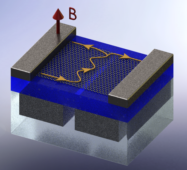
In this paper, we present a model studying the transition between graphene p-n junctions which mix Landau levels Williams et al. (2007) and those which only mix the lowest Landau level Klimov et al. (2015). We seek to further understand the magnetotransport of p-n junctions formed with buried split-gates, as depicted in Fig. (1). In order to study the effect of junction width, , on transport, we combine the delta function disorder model of Li and Shen (2008) and p-n junction interface roughness model of Low (2009), giving a simulation with more realistic conditions. We will start by introducing the details of the model, demonstrate how it can be used to replicate experimental results of Williams et al. (2007) and Klimov et al. (2015), and then present several visualizations which assist in understanding the underlying transport mechanisms.
II Background
Through the use of metal gates capacitively coupled to graphene, it is possible to create a p-n junction by locally modulating the carrier concentration. The p-n junction is a fundamental device, used as the building block from which many other devices are built. In graphene, p-n junctions exhibit very interesting physics such as Klein tunnelingKatsnelson et al. (2006) and may be used in electron optics Cheianov et al. (2007).
The application of a magnetic field perpendicular to a graphene device produces a Lorentz force which constricts transporting carriers to the edges of the sheet. A sufficiently strong magnetic field will confine the carriers into edge states, known as Landau levels, whose energy is given by
| (1) |
where is the Landau level index, given by an integer. The term is the electron charge, is the applied magnetic field, is the reduced Planck’s constant, and is the Fermi velocity (approximately ).
In a typical graphene quantum Hall measurement, the entire graphene device is uniformly doped by a global back gate and a strong magnetic field is applied. When the Fermi energy is not set to the energy of the Landau level, , the edge states on the opposite sides of the channel are isolated by an insulating bulk state. In this configuration, carrier conduction only takes place through the edges of the device. When the back gate voltage is modulated and the Fermi energy moves through the energy of a Landau level, , the bulk of the device no longer isolates the edges and electrons conduct through the entire device. These two conditions result in the transverse and longitudinal resistance, respectively, typically reported in experiments.
When a graphene p-n junction is formed, in the quantum Hall regime, the device simultaneously conducts through the edge states and localized bulk Landau levels. Away from the junction, when , carriers conduct along the edge as before. However, at the junction, where the potential of the device smoothly transitions between n and p type, there will exist an equipotential line for each transporting edge state where
| (2) |
The term is the local potential energy in the device. On this equipotential line, carriers will conduct through the bulk, bridging the edge states on the opposite sides of the channel. Furthermore, in a very smooth p-n junction, the equipotential line of each bulk state will separate, allowing one to spatially resolve conduction in each Landau level. In this work we will use quantum transport calculations to verify the condition in (2) and spatially resolve conduction through the bulk in a smoothly graded p-n junction.
Abanin et al predicted that when the Landau levels in a graphene p-n junction mix, plateaus in the two-terminal conductance will occur according to
| (3) |
where are the filling factors of the left/right sides of the junction. This effect was experimentally measured by Williams et al, where several of the predicted plateaus were observed Williams et al. (2007). The device of Williams et al was fabricated with a global back gate and local top gate, which were used to create the junction Williams et al. (2007).
There have been several studies which model the results observed by Williams et al. Tworzydło et al analyzed the importance of the valley-isospin and intervalley scattering Tworzydlo et al. (2007). Long et al Long et al. (2008) and Li et al Li and Shen (2008) both demonstrated a quantum transport model including large on-site disorder delta function potentials which allowed the Landau levels to mix and demonstrated plateaus in unipolar and ambipolar junctions. Low Low (2009) presented an alternative quantum transport model which used interface roughness, edge roughness, and localized scattering centers to mix the Landau levels, tying closely to the experiments by Williams et al Williams et al. (2007).
Recently, Klimov et al performed measurements on a graphene p-n junction which, in the ambipolar regime, only showed one plateau with a conductance of Klimov et al. (2015). This single plateau was predicted to occur when only the Landau level mixes. The device of Klimov et al was formed using a pair of split-gates buried 100 nm under the gate oxide, with a large inter-gate spacing. These split-gates produce a very graded junction profile, on the order of several hundred nanometers. The authors posited that the graded junction would spatially separate the higher order Landau levels, inhibiting mixing Klimov et al. (2015). In contrast, the top gate used by Williams et al is located very close to the graphene, producing a sharper junction Williams et al. (2007).
III Modeling techniques
In the past, quantum transport modeling has been used ubiquitously to great success in capturing the physics of graphene transport both without Low et al. (2008); Sajjad et al. (2012, 2013) and with magnetic fields presentLi and Shen (2008); Low (2009); Long et al. (2008); Golizadeh-Mojarad et al. (2008). In this work, we will use the scattering matrix (S-matrix) method, which enables us to calculate the terminal characteristics of the device in Fig. (1). Using the S-matrix method, we are also able to calculate the wave-function inside the device channel, allowing for visualizations of carrier transport. The numerical aspects of the calculations were performed using the quantum transport package KWANT Groth et al. (2014).
Carrier transport at low energies in graphene is described by a massless Dirac Hamiltonian given by
| (4) |
where is a vector of Pauli matrices and is a vector of momentum operators. This Hamiltonian may be discretized onto a honeycomb lattice, resulting in the tight-binding Hamiltonian
| (5) |
written in the language of creation/annilation operators .
The first summation in (5) fills the Hamiltonian matrix diagonals with , the on-site energy at site . The on-site energy describes the potential landscape of the device and allows the creation of a p-n junction. The second summation in (5) only generates non-zero matrix elements for lattice sites which are first nearest-neighbors, allowing transport between the sites.
Typically, is set to , representing the bond overlap between first nearest-neighbor atoms Reich et al. (2002). In this work we adopt a scaled tight-binding model, first presented in Liu et al. (2015), where the lattice constant of graphene and the hopping parameter are scaled by a scaling factor according to
| (6) |
We use a scaling factor of , which allows for more efficient simulations whilst still accurately capturing the physics of graphene.
In order to include the effect of a magnetic field applied perpendicular to the graphene sheet, we introduce Peierl’s phase by setting . A is the magnetic vector potential and the magnetic field is given by . For a device with leads oriented along the x-direction, it is convenient to define the magnetic vector potential using Landau gauge; where is the magnitude of the applied magnetic field. The effect of Peierl’s phase, in this case, is to modify the hopping parameter according to
| (7) |
where is the unperturbed hopping parameter. The integral in (7) is a line integral which takes place between the two sites and and may be calculated as a straight line, yielding
| (8) |
Simply simulating a pristine abrupt p-n junction in graphene, by putting a step in the on-site energy profile, is not sufficient to capture experimentally observed quantum Hall effects. It is necessary to include some extrinsic effects to mix Landau levels and cause inter-valley scattering at the p-n junction interface. In addition, experimentally realized p-n junctions have a finite transition between the n and p regions, the junction width , which must be included. In this paper, we present a model combining the interface delta function disorder of Li and Shen (2008), the p-n interface roughness model of Low (2009), and a finite . Our model uses disorder potential a factor of four less than that used in Li and Shen (2008). The lower disorder potential is needed to demarcate the junction profile and combined with the roughness model of Low (2009), allows us to study junction width effects in experimentally measured p-n junctions.
In our simulations, we perform an ensemble average of conductance over many randomly generated disorder profiles for a device with a fixed interface roughness profile. This procedure is used to account for ergodicity, which states that time averaging by measurements in the lab may be accounted for in simulations by ensemble averages of systems with spatial disorder Beenakker (1997).
The p-n junction profile, including effects of junction width, interface disorder, and interface roughness, are all included by modifying the on-site energy in the device channel Hamiltonian (5). We implement modifications to the on-site energy according to the piecewise function
represent the shift in the on-site energy in the device produced by capactively coupled gates. In the context of this work, a positive shift in creates a p-type region and a negative shift in creates an n-type region. The term is a delta function disorder potential placed each site, ,in the junction transition region.
The delta function disorder term, , added to the on-site energy at the sites in the junction transition region, is randomly generated according to a Gaussian distribution centered at with a standard deviation of . This site-to-site change in potential energy is sufficient to cause intervalley scattering at the junction, which is necessary to capture experimental results. The maximum disorder potential in our model is a factor of four smaller than that suggested by Li et al Li and Shen (2008). Using such a large disorder potential would obscure the effect of junction width on Landau level mixing. In our case, the disorder potential perturbs the Landau levels, but the effect of junction width will still be seen.
is the junction interface roughness profile, created using the model presented by LowLow (2009). We will repeat the specifics of the interface roughness model here for clarity. is generated as a Fourier series, given by
| (9) |
The amplitude of the Fourier component is defined as
| (10) |
The function gives a uniformly distributed random number around . The terms and the number of Fourier components, , are used to control the form of the roughness profile. In our simulations, we set and . This yields a roughness profile with an RMS standard deviation of approximately 12 nm.
Now that the device Hamiltonian (5) is fully defined, we use the S-matrix formalism to study its transport properties. We calculate the zero temperature, zero bias two-terminal conductance according to the equation
| (11) |
where the two is for spin degeneracy. The zero temperature, zero bias approximation is valid when comparing to low bias measurements performed at, or below, liquid helium temperatures. is the quantum mechanical transmission function given by
| (12) |
where the summation occurs over the S-matrix elements connecting the source and drain contacts to the channel. The calculation of the transmission function automatically includes another factor of two for valley degeneracy, which is intrinsically factored into our Hamiltonian.
In addition to calculating the conductance, we also calculate the wave functions associated with the Landau levels. By spatially resolving the wave functions, we produce maps of the transporting electron probability density, which are useful for analyzing the underlying physical mechanisms of conduction for each Landau level. The probability density at site is given by
| (13) |
where is the wave function at site for carriers from the contact. In practice, it is helpful to remove the summation in (13) and study the carriers injected by only one contact at a time.
IV Results and Discussion
We will begin by comparing the results of our model with experimental results in the literature for ambipolar junctions which mix several Landau levels Williams et al. (2007) and those which only mix the lowest Landau level Klimov et al. (2015). After verifying that our model is able to replicate results for different experimental junctions, we will seek to further understand the mechanisms at play. We will next study the effect of junction width and magnetic field strength on the degree of Landau level mixing in a junction. Several visualizations will be presented for pristine and disordered junctions which demonstrate the effect of a large junction width, where the Landau levels are separated and may be spatially resolved. Finally, we will compare a very wide junction device with analytical wave function calculations Lukose et al. (2007), demonstrating how the graded p-n junction may reveal the effect of graphene’s two sub-lattice structure. .
IV.1 Comparison with experiment
In numerically studying quantum transport, it is very important to first benchmark the model against some experimental measurements. We choose to model the experimental Hall conductance measurements of Williams et al. (2007) and Klimov et al. (2015). In an experiment, one can sweep two gate voltages independently, measuring the Hall conductance at each gate voltage. This may be continued to generate a four quadrant map of conductance for the p-n, n-p, p-p, and n-n configurations. We will focus on the ambipolar junction configuration, which is what makes graphene special compared to conventional 2DEGs.
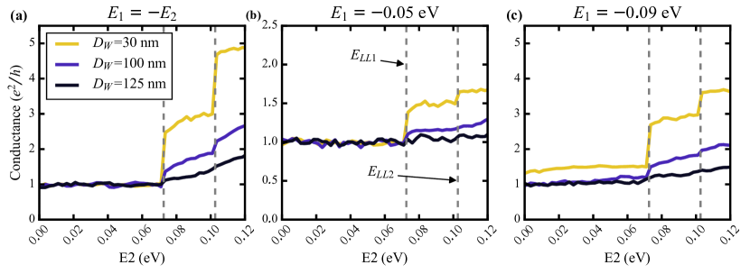
In Fig. (2) we show the simulated Hall conductance for a diagonal slice and two horizontal slices (at ) of the n-p quadrant for . The x-axis of each plot shows the on-site shift of the right side of the junction, . This shift in the on-site energy represents the effect of a charged gate nearby the graphene sheet.
Each curve in Fig. (2) is the ensemble average of 400 different randomly generated disorder configurations. There is an applied magnetic field of 4 T perpendicular to the graphene sheet. The device scattering region is 200 nm wide and 320 nm long. In this case, we choose a sheet with zigzag edges, but with our disorder model, armchair edges would yield very similar results.
When the junction width is 30 nm, our simulation recovers the first three plateaus predicted by (3), which were first measured in Williams et al. (2007). The plateaus occur at the energy levels predicted by (1), denoted by vertical lines in Fig. (2). At a junction width of 100 nm, we observe partial mixing of the first and second Landau levels. The plateaus are still visible, but occur at smaller values of conductance.
As we increase the junction width to 125 nm, there is a slight increase in conductance for filling factors of 6 and 10 in the diagonal slice, but plateaus no longer form. For the horizontal slices at , the conductance is nearly flat at 1 . This result is consistent with what was measured by Klimov et alKlimov et al. (2015).
IV.2 and magnetic field dependence
Now that we have demonstrated that our model is able to capture the experimental Hall conductance of Williams et al. (2007) and Klimov et al. (2015), we will seek to explain the differences between the two. The device which showed several plateaus Williams et al. (2007) was fabricated using a global back gate and local top gate to form a p-n junction. The device which showed a single plateau Klimov et al. (2015) was fabricated using two buried gates. The top gate is located very close to the graphene layer and produces a very sharp junction. Conversely, the buried gates are located under a thick oxide layer and have a large spacing between them. This configuration of buried gates yields a long junction width.
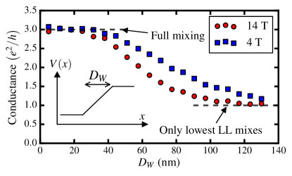
In Fig. (3) we demonstrate the dependence of Landau level mixing on junction width and applied magnetic field. We simulate the same configuration as in Fig. (2), but this time we fix the device as a symmetric n-p junction with and vary the magnetic field and junction width. Each point is an ensemble average of 400 simulations with different realizations of disorder, with a fixed interface roughness profile.
For small junction widths, less than 40 nm, the simulations display full mixing of the Landau levels. For long junction widths, approximately 100 nm and greater, only the lowest Landau level mixes. In between the full mixing and and lowest level mixing regime, the conductance smoothly decreases with junction width.
Furthermore, the applied magnetic field can control the degree of Landau level mixing. We observe that for an applied magnetic field of 14 T, it is significantly easier to inhibit mixing at the junction. This is due to increased confinement of the Landau levels at higher magnetic fields, which reduces the junction width required to fully separate the Landau levels.
IV.3 Landau level mapping
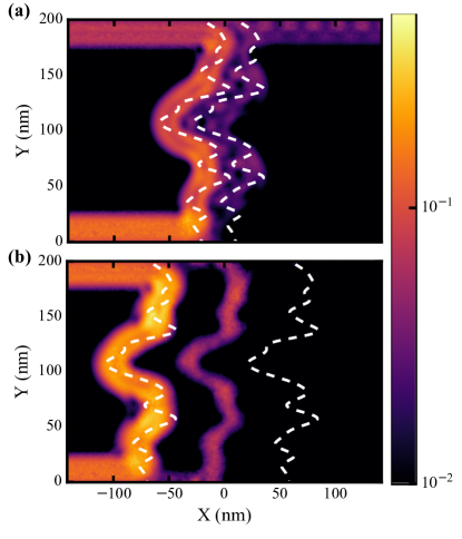
Here we will investigate the effect of junction width, , on the distribution of Landau levels transporting across the junction. In Fig. (4) we plot the non-equilibrium electron density injected from the left contact for . The device is configured as a symmetric n-p junction in a filling factor of and on the left and right sides of the junction, respectively. The maps include the full model with a roughness profile given by (9) and the delta disorders inserted randomly between the dotted white lines.
In Fig. (4), the current travels along the bottom edge from the left contact, runs up the junction, and then turns either left or right at the top edge of the device. In the case of , the and Landau levels mostly run on top of one another up the junction. There is a small separation in the levels, but much of the density overlaps. This map represents a junction which mixes higher order Landau levels and corresponds to a device which shows plateaus in the Hall conductance.
In the lower panel of Fig. (4) we show a junction width of 125 nm. In this case, the and levels are fully separated at the junction. The level is located at the center of the junction, while the level is located at the left edge of the junction. This density map represents a device which only mixes the lowest Landau level, showing a single plateau in the ambipolar configuration. The spatial separation of Landau levels inhibits mixing at the junction, which is consistent with what was proposed by Klimov et alKlimov et al. (2015).
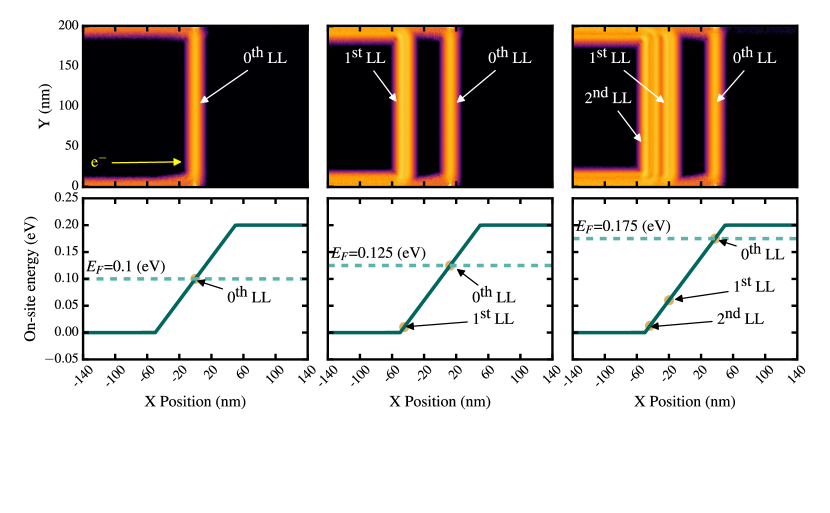
Now that we have shown visualizations of the two classes of devices, those which mix many Landau levels and those which only mix the lowest Landau level, we will explore what determines the Landau level spacing. In Fig. (5) we demonstrate a series of pristine density maps for the same potential profile, but with different Fermi levels. The three maps show a symmetric n-p junction (), and two asymmetric n-p junctions ( and ). To examine the distribution of Landau levels more easily, we demonstrate these junctions without p-n interface roughness or delta disorder potentials.
The lower panels of Fig. (5) show the energy band diagram of the junction, with the Fermi energy and corresponding Landau level energies. The position of the points for each Landau level is determined by the condition in (2). The condition in (2) also determines, within a few nanometers, where the current in the particular Landau level will turn at the junction. As the Fermi energy is increased in Fig. (5), the Landau level moves from left to right, according to (2). When the energy of the first and second Landau levels is bigger than the on-site energy, , they begin to transport. The spacing between different Landau levels is fixed by the slope of the junction potential and follows the same parabolic form as given by (1). We note that (2) works very well for predicting the turning point of the Landau levels, even without correcting the energy eigenvalues for electric field effects Lukose et al. (2007).
IV.4 Landau level shape
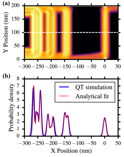
Close examination of Fig. (5) shows that higher order Landau levels split into multiple beams of carriers when they transport up the junction. The carriers do not simply travel at the junction as a Gaussian wave packet. The same effect may be seen in Fig. (4), although it is slightly more difficult to see due to junction disorder. To investigate this effect, in Fig. (6(a)) we show carrier density calculations for a symmetric n-p junction configured so that . A junction width of 500 nm is simulated, which allows us to separately spatially resolve the first four Landau levels. Note that we zoom in to only show the left side of the junction, to more easily see the Landau levels.
The higher order Landau levels shown in Fig. (6) do not follow the simple Gaussian form of the Landau level, but instead split into a more complex structure. The shape of the Landau levels is influenced heavily by the A-B sub-lattice structure of graphene, where the Landau level is formed by the superposition of the wave functions from the A and B sub-lattices.
In Lukose et al. (2007), a closed form solution for the wave function of a graphene sheet with crossed electric and magnetic fields was obtained. The system studied by Lukose et al. (2007) is similar to ours, but the electric field in their work is pointed perpendicular to the edges of their graphene sheet. Despite this difference, their analytically calculated wave function may be compared to our simulated wave function when the junction width is very long. The wave function, adopted from Lukose et al. (2007), is given by a two component spinor
| (14) |
where
| (15) |
The term , where is the applied electric field.
The wave function takes on the form of quantum harmonic oscillator functions, , where one sub-lattice contributes the harmonic oscillator function and the other sub-lattice is . The index is an integer equal to the particular Landau level number. The Landau level is contributed by one sub-lattice and is a Gaussian.
In Fig. (6(b)) we show a slice of the simulated Landau level map at . We also calculate the probability density from (14), , where is a normalization function used to match to the multi-moded transport in our simulation. We define the electric field for the analytical calculation as .
For the very long junction width considered in Fig. (6), the wave function given by (14) may be applied to our simulations. The quantum transport simulation and analytical solution of Lukose et al. (2007) agree well for the , , and Landau levels. The Landau level straddles the edge of the junction where the electric field drops to zero and the uniform electric field assumption breaks down. Nevertheless, the analytical calculation still does a good job of describing the Landau level as well.
V Conclusions
In this work we have studied the influence of junction width on Landau level mixing in ambipolar graphene p-n junctions. We utilized a combined p-n interface roughness and delta function disorder model, which represents a best case scenario to mix Landau levels. The model’s capability to match experimental data on junctions which mix several Landau levels and those which only mix the lowest Landau level was demonstrated. Our simulations indicate that more disordered devices with short junction widths are likely to mix Landau levels, while cleaner devices with very wide junction widths will only mix the lowest Landau level. To support our arguments, we provided visualizations of non-equilibrium carrier density across the junctions and a demonstrated simple predictive model which determines how the Landau levels will separate at the junction. Finally, we compared our simulations with analytical calculations Lukose et al. (2007), revealing the interesting form of higher order Landau levels. In the future, this model may be extended to more complex devices with multiple p-n junctions.
Acknowledgements.
The authors acknowledge financial support provided by the U.S. Naval Research Laboratory (grant number N00173-14-1-G017). S. LaGasse acknowledges helpful discussion with T. Low regarding his interface roughness model.References
- Klitzing et al. (1980) K. V. Klitzing, G. Dorda, and M. Pepper, Phys. Rev. Lett. 45, 494 (1980).
- Tsui et al. (1982) D. C. Tsui, H. L. Stormer, and A. C. Gossard, Phys. Rev. Lett. 48, 1559 (1982).
- Williams et al. (2007) J. R. Williams, L. Dicarlo, and C. M. Marcus, Science 317, 638 (2007), arXiv:0704.3487v2 .
- Novoselov et al. (2005) K. S. Novoselov, A. K. Geim, S. V. Morozov, D. Jiang, M. I. Katsnelson, I. V. Grigorieva, S. V. Dubonos, and A. A. Firsov, Nature 438, 197 (2005).
- Zhang et al. (2005) Y. Zhang, Y.-W. Tan, H. L. Stormer, and P. Kim, Nature 438, 201 (2005), arXiv:0509355 [cond-mat] .
- Kim et al. (2009) S. Kim, J. Nah, I. Jo, D. Shahrjerdi, L. Colombo, Z. Yao, E. Tutuc, and S. K. Banerjee, Appl. Phys. Lett. 94, 062107 (2009), arXiv:1.3077021 [10.1063] .
- Balandin et al. (2008) A. A. Balandin, S. Ghosh, W. Bao, I. Calizo, D. Teweldebrhan, F. Miao, and C. N. Lau, Nano Lett. 8, 902 (2008), arXiv:0802.1367v1 .
- Schwierz (2010) F. Schwierz, Nat. Nanotechnol. 5, 487 (2010).
- Klimov et al. (2015) N. N. Klimov, S. T. Le, J. Yan, P. Agnihotri, E. Comfort, J. U. Lee, D. B. Newell, and C. A. Richter, Phys. Rev. B 92, 241301 (2015).
- Li and Shen (2008) J. Li and S.-Q. Shen, Phys. Rev. B 78, 205308 (2008), arXiv:0807.1157 .
- Low (2009) T. Low, Phys. Rev. B 80, 205423 (2009), arXiv:0908.1987 .
- Katsnelson et al. (2006) M. I. Katsnelson, K. S. Novoselov, and A. K. Geim, Nat. Phys. 2, 620 (2006), arXiv:0604323 [cond-mat] .
- Cheianov et al. (2007) V. V. Cheianov, V. Fal’ko, and B. L. Altshuler, Science 315, 1252 (2007).
- Tworzydlo et al. (2007) J. Tworzydlo, I. Snyman, A. R. Akhmerov, and C. W. J. Beenakker, Phys. Rev. B 76, 5 (2007), arXiv:arXiv:0705.3763v2 .
- Long et al. (2008) W. Long, Q.-F. Sun, and J. Wang, Phys. Rev. Lett. 101, 166806 (2008).
- Low et al. (2008) T. Low, S. Hong, J. Appenzeller, S. Datta, and M. Lundstrom, IEEE Trans. Electron Devices 56, 1292 (2008), arXiv:0811.1295 .
- Sajjad et al. (2012) R. N. Sajjad, S. Sutar, J. U. Lee, and A. W. Ghosh, Phys. Rev. B , 1 (2012), arXiv:arXiv:1207.6619v1 .
- Sajjad et al. (2013) R. N. Sajjad, C. Polanco, and A. W. Ghosh, J. Comput. Electron. 12, 232 (2013), arXiv:1302.4473 .
- Golizadeh-Mojarad et al. (2008) R. Golizadeh-Mojarad, A. N. M. Zainuddin, G. Klimeck, and S. Datta, J. Comput. Electron. 7, 407 (2008), arXiv:s10825-008-0190-x [10.1007] .
- Groth et al. (2014) C. W. Groth, M. Wimmer, A. R. Akhmerov, and X. Waintal, New J. Phys. 16, 063065 (2014), arXiv:1309.2926 .
- Reich et al. (2002) S. Reich, J. Maultzsch, C. Thomsen, and P. Ordejón, Phys. Rev. B 66, 1 (2002).
- Liu et al. (2015) M.-H. Liu, P. Rickhaus, P. Makk, E. Tóvári, R. Maurand, F. Tkatschenko, M. Weiss, C. Schönenberger, and K. Richter, Phys. Rev. Lett. 114, 036601 (2015).
- Beenakker (1997) C. W. J. Beenakker, Rev. Mod. Phys. 69, 731 (1997), arXiv:9612179 [cond-mat] .
- Lukose et al. (2007) V. Lukose, R. Shankar, and G. Baskaran, Phys. Rev. Lett. 98 (2007), 10.1103/PhysRevLett.98.116802, arXiv:0603594 [cond-mat] .