Graphene-based, mid-infrared, room-temperature pyroelectric bolometers with ultrahigh temperature coefficient of resistance
Abstract
Graphene is ideally suited for photonic and optoelectronic applications, with a variety of photodetectors (PDs) in the visible, near-infrared (NIR), and THz reported to date, as well as thermal detectors in the mid-infrared (MIR). Here, we present a room temperature-MIR-PD where the pyroelectric response of a LiNbO3 crystal is transduced with high gain (up to 200) into resistivity modulation for graphene, leading to a temperature coefficient of resistance up to 900/K, two orders of magnitude higher than the state of the art, for a device area of 300x300m2. This is achieved by fabricating a floating metallic structure that concentrates the charge generated by the pyroelectric substrate on the top-gate capacitor of the graphene channel. This allows us to resolve temperature variations down to 15K at 1 Hz, paving the way for a new generation of detectors for MIR imaging and spectroscopy.
I Introduction
Detecting thermal infrared radiation of room temperature (RT) objects (with spectral peak emittance10mKrus2001 ; Roga2011 ) is increasingly important for applications in astronomyRichPT2005 , healthcareJoneIEEE1998 ; AhyeAHM2016 , smart energy systemsMeij2008 , securityRudoIEEE2008 , pollution monitoringKreuS1972 , fire sensingEvan FT1985 , automotiveSimoSAA2002 and motion trackingYunS2014 . Thermal photodetectors (PDs), such as bolometers and pyroelectric detectors, have emerged as the technology of choice for RT operation, because they do not need cooling to functionRoga2011 ; LangPT2005 . Graphene is ideally suited for photonic and optoelectronic applicationsBonaNP2010 ; FerrN2015 ; KoppNN2014 , with a variety of PDs in the visibleXiaNN2009 ; MuelNP2010 ; EchtNC2011 ; EchtNL2014 ; EchtNL2015 , near-infrared (NIR)FerrN2015 ; KoppNN2014 , and THz reported to dateVicaNM2012 , as well as thermal detectors in the mid-infrared (MIR)HsuNL2015 ; YaoNL2014 ; BadiNL2014 .
Pyroelectric detectors are low-cost, un-cooled thermal PDs for the MIRKrus2001 ; Roga2011 ; LangPT2005 . They are capacitor-like structures where a pyroelectric crystal is sandwiched between two metal electrodesRoga2011 . Pyroelectric crystals are materials with a T-dependent spontaneous polarization, P [C/m2], i.e. surface density of bound chargeLangPT2005 . Around RT, a linear relation links the T variation, T, with the changes of PKrus2001 ; Roga2011 ; LangPT2005 :
| (1) |
where p [C/m2K] is the pyroelectric coefficient (for the crystallographic direction perpendicular to the electrodes). The two metal electrodes are connected through an external load resistor . In thermal equilibrium (dT/dt = 0), no current flows in the external circuit because P is constant and the charges on the electrodes compensate the bound charges at the pyroelectric surfaceLangPT2005 . However, when the detector is illuminated, the absorbed radiation heats the crystal and P changes according to Eq.1 LangPT2005 . The variation of the bound charge surface density will induce a current in the external circuitLangPT2005 :
| (2) |
where A [m2] is the electrode areaKrus2001 ; WhatRPP1986 . flows only as long as T changes (i.e. when the impinging optical power changes).
Bolometers are another class of un-cooled thermal PDs, where T variations due to incoming photons produce a change in the resistance (R) of a sensing element. This can be a thin metal layerPurkIEEE2013 , a semiconductorJeroOE1993 or a superconductorKrus2001 . Common metallic bolometers for RT operation are made of TiJuSPIE1999 , NiBrocJOPSA1946 or PtPurkIEEE2013 . PolysiliconKrus2001 ; Roga2011 , amorphous siliconTissoSPIE1994 or vanadium oxideJeroOE1993 are usually exploited for semiconducting bolometers. For fixed bias , the resistance change of the sensing element translates in a measurable change in current (I). The TCR [/K] is a key performance indicator for a bolometer, and is defined asRoga2011 :
| (3) |
The TCR represents the percentage change in resistance per Kelvin around the operating point , and corresponds in module to the normalized current change per Kelvin around the operating current (Eq. 3). The TCR in metallic bolometers is0.4/KRoga2011 , whereas for semiconducting bolometers it is higher2-4 /KKrus2001 ; Roga2011 . It follows that the output of a bolometer (measured current) is proportional to T, in contrast to the output of a pyroelectric detector (measured current) that depends on the derivative of T, see Eq.2WhatRPP1986 . However, while the TCR of a bolometer does not depend on device area, in pyroelectric detectors the output current is a function of the electrode size, as for Eq.2WhatRPP1986 . Larger electrodes allow the collection of more charge, increasing the pyroelectric current, therefore leading to a larger signal.
These differences have an impact on the suitability of both technologies for different applications. Because pyroelectric detectors are alternating current (ac) devices that rely on a variable impinging radiation, they require a chopper at 25-60HzLangPT2005 to detect stationary objects, and are thus preferentially used to detect moving targets (e.g., for automatic lighting systemsMeij2008 , electrical outlet turn-offYunS2014 , unusual behavior detectionHaraPNN2002 , home invasion preventionLangPT2005 , etc.), where they are not only able to detect the presence of a warm bodiesRoga2011 , but also to extrapolate parameters like distance, direction, or speed of movementYunS2014 . Such information can be obtained by processing the analog signals of only a couple of large (1cm2) detectorsYunS2014 . On the other hand, bolometers can be scaled to smaller sizes without any loss in TCR to make arrays of pixels for stationary imaging. Resistive micro-bolometers used in high-resolution thermal cameras range from 17x17 to 28x28 m2 in sizeRoga2011 .
Refs.VoraAPL2012 ; YanNN2012 ; HanSR2013 reported graphene-based bolometers working at T10K. However, these devices are not viable for practical applications in the mass market (as for examples above), where RT operation is needed. At RT, single-layer graphene (SLG) is not competitive as the sensing element of a bolometer, as it shows a maximum TCR0.147/KLangPT2005 , lower than both the metallic and semiconducting bolometers discussed above. Ref.BaeN2015 used reduced graphene oxide films with TCR2.4-4/K at RT, whereas Ref.Hazr2013 exploited vertically aligned graphene nanosheets to produce IR bolometers with TCR11/K at RT, the largest, to date, for carbon nanomaterialsHazr2013 . In these films, however, conduction is modulated by thermally assisted electron hopping between different sheets or localized defect sitesBaeN2015 and not by any SLG intrinsic property.
SLG, however, can play a key role when integrated in pyroelectric devices. SLG can be used as a transducer for the pyroelectric polarization due to its field-effect responseHsieAPL2012 . If a graphene field-effect transistor (GFET) is fabricated on a pyroelectric substrate, the channel resistance is modulated by the substrate polarization and can thus represent a direct T readout. This is the electrical equivalent of a bolometric response with area-independent TCR (the charge density of the pyroelectric ’gate’ is constant, and does not depend on the size and shape of the graphene channel). Ref.HsieAPL2012 reported TCR6/K for GFETs on lead zirconate titanate (PZT), a material with one of the highest pyroelectric coefficient known to date (up to 780C/m2K)GuoAPL2007 . This indicates that the pyroelectric charge density generated by PZT underneath the SLG channel is still too limited to significantly outperform state-of-the-art bolometersHsieAPL2012 .
Here, we demonstrate a RT pyroelectric bolometer for MIR with ultrahigh TCR. Our PD is a two-terminals device whose resistance changes proportionally to T, like a bolometer. Internally, the PD comprises a floating metallic structure that concentrates the charge generated by the pyroelectric substrate over an integrated GFET. Since charge cannot escape from the floating structure (i.e. there is no load resistor), the PD can be operated in direct current (dc) and there is no need for chopping. The total pyroelectric charge generated upon a variation in T increases with area, delivering TCRs up to 900/K for a footprint of 300x300m2, 2 orders of magnitude larger than state-of-the-art IR detectors having any similar or larger areaKrus2001 ; Roga2011 ; BaeN2015 ; Hazr2013 . The TCR scaling is sub-linear for smaller footprints. We discuss the origin of this behavior and conclude that our device performance is competitive even in the limit of very small pixels.
II Results and Discussion
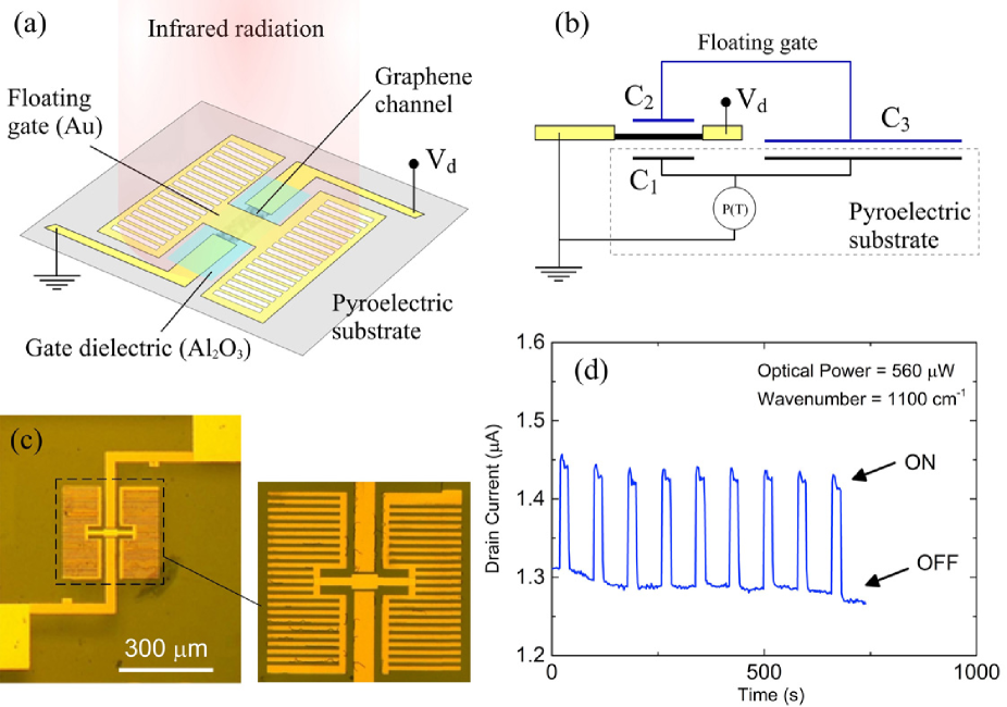
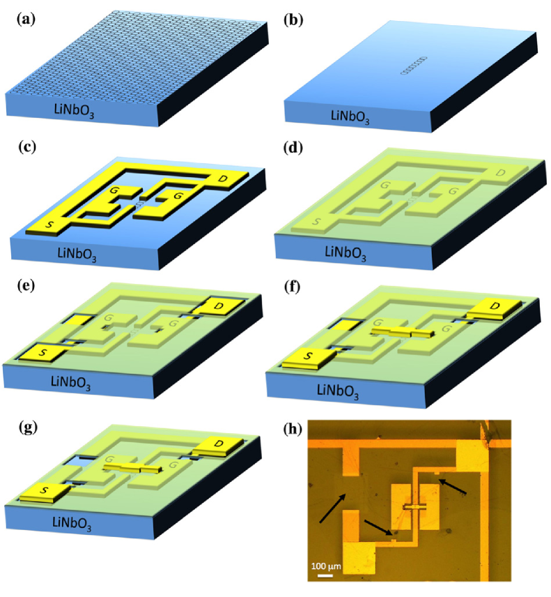
Figs.1a,b show the layout of a single device and the corresponding electrical model. A SLG channel with source and drain contacts is fabricated on a pyroelectric substrate: 500m-thick z-cut LiNbO3 (LN) crystal, as described in Methods. A 10 nm-thick Al2O3 dielectric layer isolates the SLG from an H-shaped floating Au structure designed to overlap the oxide-coated SLG in the center, while lateral pads are placed in direct contact with the substrate. Both uniform and patterned Au pads have been studied, the latter in the form of finger-like structures (in order to enhance light absorption at selected wavelengths, see Methods). The design is such that the SLG channel conductivity can be modulated by a dual-gate capacitive structure. From the bottom, there is the pyroelectric polarization (and associated electric field) generated directly by the substrate ( in Fig.1b), which we refer to as the ’direct effect’ on graphene conductivity (previously exploited in Ref.HsieAPL2012 ). From the top, there is a gate connected in series with capacitor as a floating circuit branch, with . The perimeter of the pads defining sets the overall pixel size, from which only the source and drain contacts stem out to interface with the measurement electronics.
In first approximation, the generated pyroelectric charge Q is uniformly distributed on the substrate upon a T variationKrus2001 ; Roga2011 . Therefore, the direct effect from does not depend on the channel area , since the bottom gate field depends on the pyroelectric polarization, which is constant over any area. For the floating gate in Fig.1b, Q accumulating on depends on area as (from Eq.1) . Being the structure electrically floating, the same Q will be stored on , generating an effective top-gate voltage (in module):
| (4) |
where , and are the vacuum and relative permittivity, and t is the oxide thickness. For fixed t and T, controls the amplification through the top gate voltage driving the GFET, modulating the graphene drain current.
Fig.1c shows an optical micrograph of a device with patterned pads. We illuminate this device with MIR radiation at 1100cm-1 (9m) using a laser spot matching the pixel size (300x300m2). The resulting modulation of the channel drain current is shown in Fig.1d over 9 ON/OFF laser cycles. A responsivity0.27mA/W is obtained, for a drain current in the dark ()1.3A (=10mV). The responsivity can be increased by applying a larger , which in turns increases . The normalized current responsivity in [/W] is defined as:
| (5) |
where is the current under illumination and is the optical power of the incoming radiation. This is a better parameter to compare photoconductive detectors. in Fig.1d is/W, over two orders of magnitude higher than in Ref.HsieAPL2012 , where only the direct effect was exploited (/W)HsieAPL2012 .
By reducing the laser spot to 10m and using a lock-in, we produce photocurrent maps of a single pixel to assess where the maximum signal is generated (Figs.2a-d).
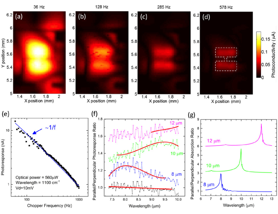
At the slowest chopper frequency (f=36Hz, Fig.2a) the photocurrent map shows two broad peaks (700m), which largely overlap and extend beyond the pixel area. When f is increased, the two peaks become progressively resolved until, above 500 Hz (Fig.2d), they match the location of the lateral pads defining the pixel. These are not necessarily the areas where the strongest absorption occurs, but those where T changes are detected providing the highest photocurrent . Figs.2a-d also show that the signal decreases at higher f. To better quantify this trend, we plot upon full illumination (300x300m2 spot size, Fig.2e) as a function of f. scales linearly with 1/f and is measurable up to 1kHz. This PD can be described by a thermal model, see Methods. This confirms the most intuitive interpretation of the measurements. When an increase in illumination time per cycle (i.e. a reduction in f) results into a proportional T increase, the system is far from a dynamic equilibrium with the thermal sink (the chip carrier) within a single cycle. This behavior is observed for f60Hz. Also, since at slow chopping speeds (Fig.2a,b) there is more time to approach dynamic equilibrium, including to laterally spread away from the illuminated spot, the T within the pixel becomes more homogeneous, resulting in blurred photomaps.
All results presented so far are for monochromatic illumination at 1100cm-1 (9.1m,136meV). Fig.2f plots the wavelength dependence of the photocurrent for devices with lateral pads patterned with a finger-like design (as in Fig.1c) with different pitches. The fill ratio (i.e. Au finger area/total available pad area) is kept constant at 0.5, meaning that, e.g., fingers with an 8m pitch are 4m-wide and separated by a 4m gap. While for a uniform Au pad the photoresponse to parallel and perpendicular light is the same for all wavelengths (black data in Fig.2f), for patterned pads a peak arises in the parallel/perpendicular photoresponse ratio at the wavelength that matches the fingers pitch.
We then simulate the total parallel/perpendicular absorption for finger-like Au structures on thick LN (Fig.2g, see Methods for details). This shows that a peak is expected at the wavelength corresponding to the fingers pitch. This is consistent with Fig.2f, as more absorption results into a larger T increase, therefore a larger signal. In the calculations we assume that all light entering the bulk LN substrate is eventually absorbed, contributing to the T rise. Parallel-polarized light gets more absorbed overall (i.e. in the Au fingers plus LN substrate) than the perpendicular-polarized light, despite the fact that at the resonant frequency the perpendicular-polarized light is absorbed more inside the Au fingers (see Methods). The reason for this is that resonant absorption in the fingers is also accompanied by resonant reflection (RFL), which lowers the overall delivery of light into the Au/LN system as 1-RFL. Things would change if these devices were fabricated on pyroelectric layers1m thick (rather than a 500m LN crystal). The absorption of the resonant structures would become dominant over the intrinsic absorption of the substrate and reflectance would play a minor role. Fig.2f proves that our device layout is well suited for the implementation of photonic structures to engineer photon absorption and that a spectrally-selective MIR response is feasible.
The data in Figs.2 suggest that even better results could be obtained for devices with an optimized thermal management compared to that offered by a bulk 500m-thick pyroelectric substrate. Isolated pixels with lower heat capacity, using thin suspended bridges or membranes (as routinely done for microbolometers, with typical thickness1mRoga2011 ), would further boost responsivity, speed and wavelength selectivity.
We now consider the performance as local thermometer, independent from the conversion of photons to T (linked to the emissivity and to the thermal properties of the device, such as thermal capacity and thermal conductanceRoga2011 ; WhatRPP1986 ). Each pixel is a two terminal device whose resistance represents a readout of the local T. As for bolometersRoga2011 , we consider the TCR as the figure of merit. Being a normalized parameter, the TCR does not depend on . For our devices it depends on pixel area, so we will link each TCR value to the size of the corresponding pixel. Furthermore, since our variations in resistance are the result of a gain mechanism, we consider how they compare to the device noise. We introduce the noise equivalent substrate temperature (NEST), i.e. the pixel T change needed to produce a signal equal to the amplitude of the noise. This is not to be confused with the noise equivalent T difference (NETD)Krus2001 , often used to indicate the smallest detectable T change in an IR-emitting body imaged by a PD, also dependent on the photon-to-T conversionKrus2001 .
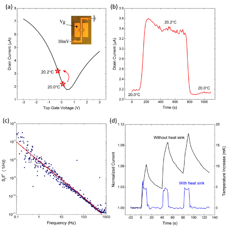
In Fig.3a,b we investigate the thermo-electrical characteristics of a representative device (pixel size: 100x100m2, =22) by placing the sample on a chuck with T control. Since for these measurements the sample is in thermal equilibrium in the dark and photon absorption plays no role, uniform Au pads are chosen to accommodate (when needed) an electrical probe on the gate pads and apply an external . Fig.3a plots a typical Dirac curve for a GFET at T=20∘C. Note that, when an active electrical probe is connected to the gate pad, this neutralizes any charge coming from and the transfer characteristics are equivalent for all devices ( is fixed at 22x20m2). The vast majority of our devices are slightly p-doped (hole density2.5-31012cm-2, in agreement with our Raman data, see Methods), which is ideal to achieve a maximum signal upon heating. This is linked to our choice of placing the SLG on the positive face of z-cut LN, where heating reduces the net dipole moment, equivalent to a negative LangPT2005 .
After removing the gate probe to leave the gate structure floating, we monitor the GFET drain current while T is raised by 0.2∘C, kept constant for 10 minutes, then decreased to its original value. Fig.3b shows that the drain current increases by50 for a 0.2∘C T change (TCR250/K), it is stable over time, and then returns to its original value with negligible hysteresis. The red star markers in Fig.3a show how the SLG conductivity evolves when the gate is thermally driven as in Fig. 3b. This stable DC response over several minutes indicates that no appreciable leakage occurs through the pyroelectric crystal and/or the GFET gate within a practical measurement timeframe. The initial bump to 3.6A in Fig.3b is due to the small overshoot of the chuck T at the end of the ramp.
In order to evaluate the NEST we measure the normalized noise power spectrum for a representative device (Fig.3c). The spectrum is dominated by 1/f noise up to 1kHz and closely resembles those previously measured for SLG devicesBalaNN2013 . The channel area (LxW) normalized noise ()(LxW) is510-7 m2/Hz at 10Hz (considering our 20x30m2 channel), which slightly exceeds the typical range (10-8-10m2/Hz) reported for SLG devices on SiO2BalaNN2013 . Considering a pixel size of 100x100 m2 and a TCR214/K, we get for the device in Fig.3b a NEST40K/Hz1/2 at 1Hz (NEST=/TCR). For the biggest pixel size (300x300m2, TCR600/K), the minimum NEST is15K/Hz1/2. For the MIR PD in Fig.1, this T resolution translates into a noise equivalent power (NEP)510-7W/Hz1/2 at 1Hz (NEP=/RphN), almost one order of magnitude better than Ref.KulkOM2015 and a very promising number considering the limitations in terms of thermal conductivity and mass.
To appreciate what these numbers mean in practice, we plot in Fig.3d the photoresponse of a large device (300x300m2, TCR600/K) illuminated by the IR radiation emitted by a human hand at a distance15cm. In one test the sample sits on a large (200mm diameter) metal chuck (with heat sink, blue data), and in another it is placed in a concave plastic box that keeps it suspended, thus more thermally isolated (without heat sink, black data). Without heat sink, the PD heats up more (hence larger device responsivity), but its response and recovery are much slower. Even with heat sink, the proximity of the hand is easily detected. The saturation signal is3, corresponding to a T increase5mK. For the sake of comparison, to the best of our knowledge, the only RT SLG detector working at 10m and able to allow human hand detection is described in Ref.HsuNL2015 . This was fabricated on a suspended and very thin (1m) SiN membrane, measured in vacuum and with a lock-in with 10s integration timeHsuNL2015 . Here we achieve the same result on a bulk (500m-thick) substrate with a resistive measurement in air for 200ms, indicating that our SLG-based pyroelectric bolometer can provide far better performance (in terms of responsivity and speed) in equivalent conditions.
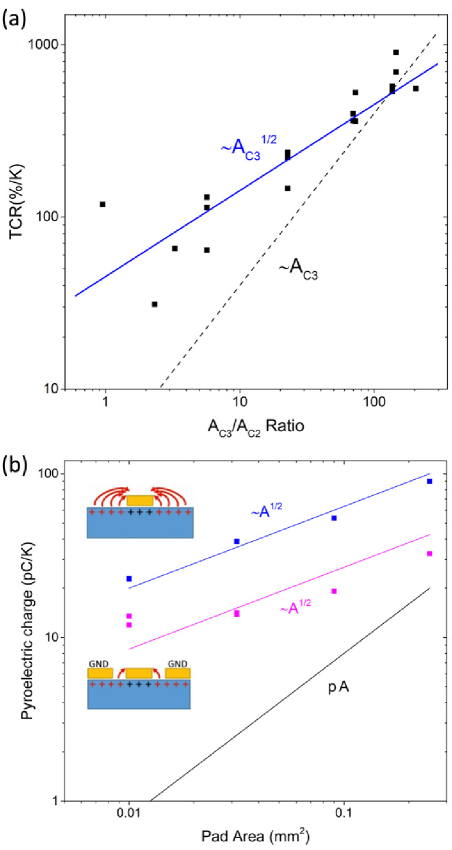
Finally, we discuss how our TCR scales with . Fig.4a plots the measured TCR for 18 devices fabricated by keeping constant (22x20m2) and varying from 25x25m2 to 300x300m2. Under our design assumptions (and disregarding ), the TCR should be proportional to the pyroelectric charge generated by , hence, from Eq.1 one would expect a linear relation TCR. Our data, however fit a square root dependence, indicated by the blue line. This behavior cannot be explained by invoking the direct effect, whose contribution appears on a much smaller scale (TCR5/K, see Methods). Rather, we have to consider that the pyroelectric substrate does not end at the pads edge. Such pads are thus not driven just by the crystal below them (as assumed by a linear dependence on area), but can also be affected by the exposed polarization of their surrounding areas (an effect scaling linearly with perimeter, hence the square root dependence on area). To better quantify this behavior, we prepare Au pads of different size (0.01-0.3mm2) on our pyroelectric substrates and measure the total charge generated upon heating (Fig.4b). This is accomplished by placing an electric probe on each pad, connecting the probe to ground and integrating the pyroelectric current flowing through the probe over the whole temperature ramp. In one case, the pads are kept isolated on the 1x1cm2 pyroelectric surface and independent from each other. In another case, the whole surface around the pads is coated with Au and grounded during all measurements (with only a gap of 5m uncoated around the pads). This is meant to suppress any contribution from areas beyond the pad footprint. Fig.4b, however, shows that a square root dependence on pad area is observed in both cases. The total pyroelectric charge decreases by a factor2-3 upon screening, but is still above what would be expected from the modelRoga2011 , Q/T=p A, even for relatively large pads (using p=77C/m2K, as measured for a LN sample fully covered with Au and consistently with literatureRoga2011 ; LangPT2005 ; Wong2002 ). This result has major technological implications, since it proves that a substantial contribution to the observed TCR enhancement for small arises within the first few microns from the pad edge. It is then possible to harvest an enhanced pyroelectric charge in a dense array of small pixels, with only a gap of few microns separating two adjacent devices.
In principle, is desirable to deliver TCRs up to 900/K (Fig.4a, see also Methods), but this upscaling is bound by the maximum gate voltage variation allowed for the GFET (dynamic range). When probed electrically (Fig.3a), our GFETs show no gate leakage up to 5V (5MV/cm). Beyond this value dielectric breakdown can occur. This determines the maximum thermal shock a device can sustain without failing, inversely proportional to the TCR. However, it is not a concern if the environment T is drifting on a time scale much larger than the measurement timeframe, e.g. during a day/night indoor T cycle. While internal pyroelectric leakage can be neglected over a few minutes, it can still discharge a device over longer times. This will always leave the GFET at the best operating point to respond to sudden signals (see Methods). If one wants to scale down the pixel size while maintaining the same area ratio, the channel area must be decreased accordingly. Since the 1/f noise scales with channel areaBalaNN2013 , we expect the GFET noise to increase and cancel the benefit of a large TCR when the NEST is evaluated. Fig.4 however shows that the TCR scales sub-linearly with area. For pixels approaching the scale required for high resolution (20x20 m2) IR camerasRoga2011 , it is better to make a large (several m) channel and accept 10 because the small price paid in terms of TCR will be more than compensated by lower noise, less critical lithography, and a detector more resilient to sudden thermal shocks.
III Conclusions
We presented a graphene-based pyroelectric bolometer operating at room-temperature with TCR up to900/K for a device area 300x300m2 able to resolve temperature variations down to 15K at 1Hz. For smaller devices the TCR scales sub-linearly with area, due to an enhancement of the collected pyroelectric charge in close proximity to the metallic edges. When used as mid infrared detectors, our devices deliver very promising performance (in terms of responsivity, speed and NEP), even on bulk substrates, and are capable to detect warm bodies in their proximity. Spectral selectivity can be achieved by patterning resonant structures as part of the pixel layout. This is competitive on a number of levels, ranging from high-resolution thermal imaging (small pixels) to highly-sensitive spectroscopy in the mid- and far-IR (large pixels).
IV METHODS
IV.1 Devices fabrication
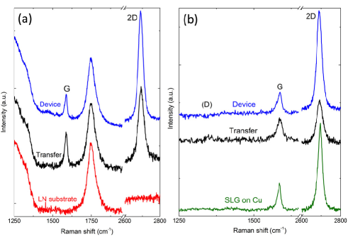
SLG is grown by chemical vapor deposition (CVD) on 35-m-thick Cu following the process described in Ref.BaeNN2010 . The quality of the material is monitored by Raman spectroscopy using a Renishaw InVia equipped with a 100X objective at 514.5nm, with a laser power below 300W to avoid possible heating effects or damage. Fig.5b (green curve) shows the Raman spectra of SLG on Cu. The 2D peak is single-Lorentzian, a signature of SLG, with FWHM(2D)=26cm-1FerrPRL2006 . The D to G intensity ratio, I(D)/(G)0.1 indicates a defect density2.51010cm-2FerrPRL2006 ; CancNL2011 ; FerrNN2013 ; FerrPRB2000 . SLG is then transferred on the positively charged surface of z-cut LN (Roditi International Ltd) by spin coating a 500nm-layer of polymethyl methacrylate (PMMA) and then etching the Cu foil with an aqueous solution of ammonium persulfateBaeNN2010 . The resulting graphene/PMMA film is rinsed in water and picked up with the target substrate. After drying, the sample is placed in acetone to dissolve the PMMA, leaving a film of SLG on LN. Fig.5a plots the Raman spectrum after transfer on LN (black curve). The spectrum for the bare LN substrate is also reported (red curve). The D peak region at1350cm-1 is convoluted with an intense band at 1200-1450cm-1 arising from optical phonons in LNBarkPR1967 . An additional LN peak is also present at 1744 cm-1, which does not overlap with any of the characteristic features of SLGBarkPR1967 . In Fig.5b we plot the transferred SLG spectrum (black curve) after subtracting the reference contribution of the LN substrate, and normalization to the LN peak at 1744cm-1. The 2D peak is single-Lorentzian with FWHM(2D)38cm-1. The position of the G peak, Pos(G), is 1588cm-1, while its full width at half maximum, FWHM(G), is14cm-1. The position of the 2D peak, Pos(2D), is 2691cm-1. The 2D/G peak intensity and area ratios, I(2D)/I(G) and A(2D)/A(G), are 2.1 and 4.1, respectively, suggesting a doping concentration51012cm-2 (300meV)DasNN2008 ; BrunACSN2014 ; BaskPRB2009 . The spectra show I(D)/(G)0.22, corresponding to a defect concentration5.41010cm-2FerrPRL2006 ; CancNL2011 ; FerrNN2013 ; FerrPRB2000 , similar to that before transfer, indicating that negligible extra defects are introduced during the transfer processFerrPRL2006 ; CancNL2011 ; FerrNN2013 ; FerrPRB2000 .
The fabrication of top-gated GFETs on LN presents additional challenges compared to Si/SiO2. Owing to the pyroelectric nature of LN, a significant static charge can build on both surfaces. To preserve our devices from discharge-induced damage, we initially prepare all metallic features on the LN surface as an electrically connected pattern, i.e. source, drain and floating gate contacts of the GFET are shorted together by means of metallic lines. In this configuration the device can undergo all the required high-T (up to 120∘C) processing steps without failing. The shorts are then removed in the last step, when no further heating is required aside from normal sensor operation. The device fabrication process is outlined in Fig.6. First, SLG channels are patterned (Fig.6b) using optical lithography and dry etching in O2 (20W for 20s). A second lithographic step defines the metal contacts (source and drain), as well as the floating gate pads directly in contact with the substrate (Fig.6c). Note that all features are shorted together as explained above. Before the deposition of a 40nm-thick Au layer via thermal evaporation, a mild Ar plasma (0.5W, 20s) is used on the exposed SLG areas. This is crucial to achieve a good contact resistance (100), as defects induced by the plasma ensure a good bonding with the metalChoiJAP2011 . Further, a 10nm Al2O3 layer is deposited by atomic layer deposition (ALD) at 120∘C, to serve as gate dielectric (Fig.6d). 2nm Al is used as seed layer for ALDKimAPL2009 . Optical lithography is again used to define apertures in the Al2O3 in order to expose the contact pads (source and drain), part of the shorting lines and a small section of the lateral pads where the top electrode needs to be anchored. The Al2O3 is then wet-etched in an alkaline solution (D90/H2O 1:3) for6 minutes, leaving the structure in Fig.6e. Another lithographic step is then used to finalize the top-gate structure via thermal evaporation and lift-off of 2/60 nm of Cr/Au. Bonding pads are also prepared in this step, overlapping with those deposited with the contacts (Fig.6f). Finally, the electrical shorts are removed with a last lithographic step followed by wet-etching of the Au lines in an aqueous solution of KI/I2 (Fig.6g). An optical picture of the final device is shown in Fig.6h, the arrows indicating where the Au shorts have been etched. Fig.5a shows the Raman spectrum after the device fabrication (blue curve). The laser spot is in the gap between a contact and the top-gate. LN peaks (1200-1450cm-1 and 1744cm-1) appear as a signature of the underneath substrateBarkPR1967 . The spectrum after subtracting the LN reference is presented in Fig.5b (blue curve) and compared with graphene after transfer (i.e. before fabrication, black curve). The signature of SLG is again confirmed from the single-Lorentzian line-shape of the 2D peak with FWHM(2D)31cm-1FerrPRL2006 . Pos(G)=1584cm-1, FWHM(G)16cm-1 and Pos(2D)=2689cm-1. I(2D)/I(G) and A(2D)/A(G) are 4.2 and 8.5, respectively, indicating a doping level200meV (1012cm-2)DasNN2008 ; BrunACSN2014 ; BaskPRB2009 . The doping due to Al2O3 encapsulationHoACSN2012 is consistent with the value extracted from the electrical data in Fig.3. From I(D)/I(G)0.16, a defect concentration41010 cm-2 is obtainedFerrPRL2006 ; CancNL2011 ; FerrNN2013 ; FerrPRB2000 . This indicates that the fabrication process does not introduce defectsFerrPRL2006 ; CancNL2011 ; FerrNN2013 ; FerrPRB2000 .
IV.2 Device Characterization
T-dependent electrical characterization is performed with a Cascade probe station with a T-controlled chuck, coupled to an HP4142B source-meter. The spectral density of the current fluctuations (SI) is the Fourier transform of the drain current recorded during 100s with a sampling of 1ms. The normalized SI/I2 has the same 1/f dependence for all drain voltages.
The devices are then illuminated by a linearly polarized quantum cascade laser with a frequency range from 1000 to 1610cm-1 (6.2-10m) scanned using a motorized xyz-stage. The laser is modulated using a chopper and the current measured with a current pre-amplifier and lock-in amplifier. The light polarization is controlled with a ZnSe wire grid polarizer. The light is focused using ZnSe lenses with NA0.5. The power for each frequency is measured using a bolometric power meter and the photocurrent spectra are normalized by this power to calculate the responsivity.
IV.3 Simulations and Models
Optical calculations are performed with a finite-difference time-domain (FDTD) methodTafl2005 ; LidoJAP2007 assuming an infinite array of infinitely long Au fingers (40nm-thick) on a semi-infinite LN substrate. Thermal transient calculations are performed with a finite element method (FEM)Comsol assuming a 500m-thick LN substrate on a 3mm-thick Au block (heat-sink) whose back surface is kept fixed at room temperature.
Fig.2e shows that, when a chopper induces a periodicity in the illumination (and associated heating), the amplitude of the resulting periodic photoresponse scales linearly with the inverse of its frequency. We present here a thermal model and associated simulations to explicitly study the time-dependent heating and cooling properties of our device and confirm the above conclusion.
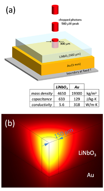
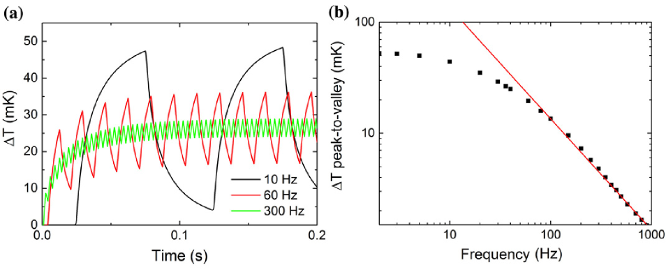
Fig.7a illustrates how we model the experiment in Fig. 2e. A laser beam with equivalent characteristics (560W, 300m in diameter) is chopped at variable frequencies with a 50 duty cycle. The 500m-thick LN substrate is in contact with a 3mm-thick Au layer (that represents the chip carrier), acting as heat sink towards a boundary at fixed temperature T0. Typical materials parameters are reported in Fig.7aRoditi . We make the following approximations: 1) Real devices with patterned Au pads reflect50 of the impinging light. We thus assume 50 reflectance for the LN film and 0 transmission (i.e. 50 absorption); 2) We assume radiation uniformly absorbed in the LN film; 3) we disregard heating losses by convection and radiation. Under these assumptions, the T distribution near the laser spot for an arbitrary instant in time is shown in Fig.7b.
Fig.8a shows the simulated temperature transient T=T-T0 for the point at the top of the LN film and at the centre of the illumination spot. The average T saturates atT0+50mK for all frequencies, because this would be the equilibrium value for constant illumination at 280W (the impinging power is 560W/2 at all frequencies). The photoresponse measured by the lock-in in Fig.2e overlooks this average T and reflects the peak-to-valley T of a single period, in phase with the chopper. This, on the other hand, varies significantly in Fig.8a for the three frequencies reported. The full dependence of the T peak-to-valley on f is shown in Fig.8b. The calculations are performed with a finite element method (FEM)Comsol using the assumptions made for Fig.7. Despite the approximations, our simulations reproduce the 1/f behavior observed experimentally above 60Hz in Fig.2e. For low frequencies (10Hz), the system saturates within one period.
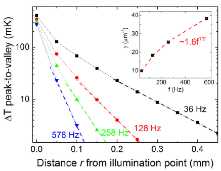
To match the conditions used for the photomapping in Fig.2a-d, we now reduce the spot diameter to 10m and increase the laser power to 1.8mW. Fig.9 shows the T peak-to-valley for a number of points on the LN surface as a function of their distance, r, from the centre of the illumination spot. Outside the spot, T decays with a rate that depends on f. A decay of the formexp(-r) is found, with =1.6f1/2. This means that the higher f, the less the heat delivered by the laser in one cycle is allowed to spread radially. For this reason, the photomapping in Fig.2d is much more resolved than in Fig.2a.
IV.4 Wavelength-selective absorption
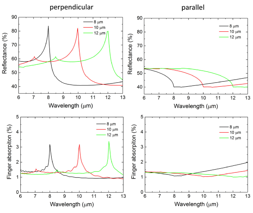
Fig.2f indicates that the photoresponse of a device with lateral pads patterned as parallel fingers with pitch L and filling ratio 0.5 exhibits a peak in the ratio between parallel and perpendicular incident light. The spectral position of such peak is linked to the geometrical parameter L. Fig.2g shows that the total absorption (linked to the device photoresponse) has peaks in the parallel/perpendicular ratio at wavelengths that closely match the experiment. However, Fig.2g does not allow to discriminate between reflectance, pattern absorption and substrate absorption, i.e. the individual components contributing to the total absorption.
Fig.10 plots the simulated reflectance and absorption in the Au fingers for both parallel and perpendicular polarized light for L=8, 10, 12m, as in Fig.2f,g. For both reflectance and finger absorption, peaks are found at the corresponding wavelength. Reflectance and finger absorption are measured as of the total incident light. This means that, even if more light is reflected at resonance for perpendicular polarization, this is also the condition that results in maximum absorption in the fingers. However, peak absorption in the fingers at resonance is3 for perpendicular polarization (versus1 off-resonance and for parallel polarization), while the measured absorption of a 500m-thick LN substrate is75 in this wavelength range. Hence, substrate absorption dominates, overshadowing the absorption features in Fig.10, and the total absorption is determined by 1-RFL. In the limit of thin substrates, however, which is the case of highest technological interest, the photoresponse will strongly depend on the absorption in the fingers, and simulations like that in Fig.10 will be crucial to optimize the design of patterns to enhance absorption and spectral selectivity.
IV.5 Characterization of the direct effect
We now investigate the conductivity modulation induced by the substrate (direct effect) in devices where the floating top-gate is omitted. We deposit the Al2O3 dielectric layer in all cases, to improve device stability. We extract the TCR by means of thermo-electrical measurements, as in Fig.3b, but with T ramp expanded to 1∘C, because of the weaker response.
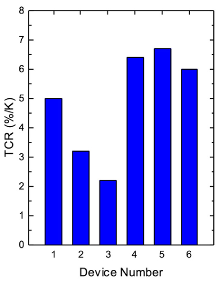
Fig.11 plots the TCR distribution across multiple devices with equivalent geometry. The average TCR (in module) is 4.9/K, on par with that reported by Ref.HsieAPL2012 for SLG on lead titanate zirconate (6/K). Thus, the contribution of the direct effect to the device sensitivity is negligible compared to the amplified response achieved with the floating gate, which remains dominant even for the smallest pixel size (=1, see Fig.4a). This means that, in most practical cases, there is little benefit in placing SLG in direct contact with the pyroelectric substrate. We envisage that the performance of our devices can be further optimized by implementing a suitable spacer between SLG and the pyroelectric substrate, chosen from materials known to provide a smooth and inert interface with SLG (e.g. boron nitrideDeanNN2010 ).
IV.6 Device resilience to large temperature variations
The breakdown field of the Al2O3 dielectric layer limits the dynamic range of the GFET, for a given TCR. We consider safe to apply gate fields up to 5 MV/cm, corresponding to an applied voltage of 5V for a 10-nm-thick alumina film. Close inspection of Figs.3a,b reveals that, if 0.2∘C induce a gate voltage of -0.44V, a T variation3∘C may result in device failure. All samples are subjected to much larger (10∘C) T variations. Surprisingly, the devices are very resilient, with no accidental failure and consistent response.
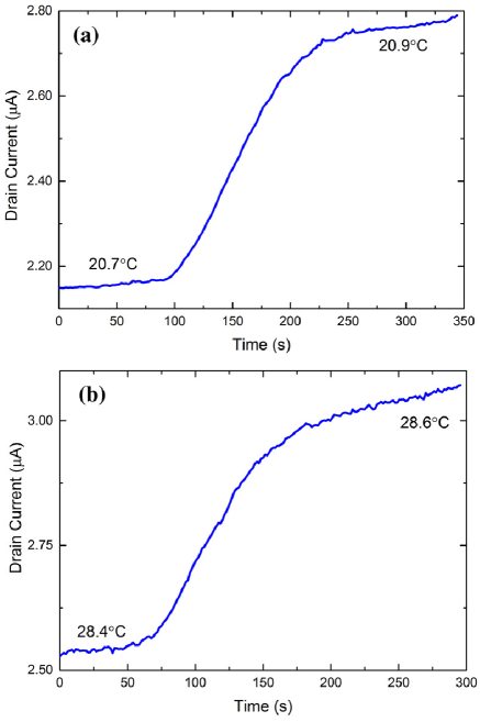
The reason for this behavior resides in the T gradient, i.e. how slow or fast the device experiences the T variation. Fig.12a plots the response of a representative device with TCR130/K as T increases by 0.2∘C in 3 minutes. This corresponds to an induced gate voltage of -0.22V (because of the different ratio, the TCR is roughly half that in Fig.3b). Accordingly, increasing T by 8∘C should result in an induced voltage9V, destroying the device. The T is thus slowly raised by8∘C with (2∘C/hour) and the response to a T variation of 0.2∘C is measured again (Fig.12b). Interestingly, not only the device survives the dielectric breakdown, but its response is still consistent with Fig.12a. Indeed, the drain current at 28.4∘C (2.53A, Fig.12b) is almost the same as previously measured at20.8∘C (Fig.12a), indicating that the operating point tends to drift in the opposite direction of the applied stimulus. This is not due to the GFET hysteresis, as this would have been evident also in Fig.3b (where no hysteresis is observed). Hence, we conclude that the drift preserving the device comes from the slow (hours) internal discharge of the pyroelectric crystal. This is negligible over a few minutes (Fig.3b), but can play an important role over several hours.
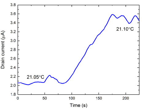
IV.7 Drain current response for large pixels
IV.8 Acknowledgements
We acknowledge funding from EU Graphene Flagship, ERC Grant Hetero2D, and EPSRC Grant Nos. EP/ 509 K01711X/1, EP/K017144/1, EP/N010345/1, EP/M507799/ 5101, and EP/L016087/1. We thank Graphenea for the provision of some CVD graphene samples on LN.
References
- (1) P. W. Kruse, Uncooled thermal imaging arrays, systems and applications (SPIE press Bellingham, WA, 2001).
- (2) A. Rogalski, Infrared detectors (CRC Press, London, 2011).
- (3) P. L. Richards, and C. R. McCreight, Infrared detectors for astrophysics. Phys. Today 58, 41 (2005).
- (4) B. F. Jones, A reappraisal of the use of infrared thermal image analysis in medicine. IEEE Trans. Med. Im. 17, 1019 (1998).
- (5) K. Ahyeon et al., Ultrathin Injectable Sensors of Temperature, Thermal Conductivity, and Heat Capacity for Cardiac Ablation Monitoring. Adv. Health. Mat. 5, 373 (2016).
- (6) G. C. M. Meijer, Smart sensor systems (Wiley, Chichester, UK, 2008).
- (7) P. Rudol and P. Doherty, Human Body Detection and Geolocalization for UAV Search and Rescue Missions Using Color and Thermal Imagery. IEEE Aerosp. 1 (2008).
- (8) L. B. Kreuzer, N. D. Kenyon, and C. K. N. Patel, Air Pollution: Sensitive Detection of Ten Pollutant Gases by Carbon Monoxide and Carbon Dioxide Lasers. Science 177, 347 (1972).
- (9) D. D. Evans, and D. W. Stroup, Methods to Calculate the Response Time of Heat and Smoke Detectors Installed Below Large Unobstructed Ceilings. Fire Tech. 22, 54 (1985).
- (10) I. Simon and M. Arndt, Thermal and gas-sensing properties of a micro-machined thermal conductivity sensor for the detection of hydrogen in automotive applications. Sens. Act. A 97, 104 (2002).
- (11) J. Yun, and S. Lee, Human Movement Detection and Identification Using Pyroelectric Infrared Sensors. Sensors 14, 80578081 (2014).
- (12) S. B. Lang, Pyroelectricity: from ancient curiosity to modern imaging tool. Phys. Today 58, 3136 (2005).
- (13) F. Bonaccorso, Z. Sun, T. Hasan, and A. C. Ferrari, Graphene photonics and optoelectronics. Nat. Phot. 4, 611 (2010).
- (14) A. C. Ferrari et al. Science and technology roadmap for graphene, related two-dimensional crystals, and hybrid systems. Nanoscale 7, 4587-5062 (2015).
- (15) F. Koppens et al. Photodetectors based on graphene, other two-dimensional materials and hybrid systems. Nature Nano 9, 780 (2014).
- (16) F. Xia, T. Mueller, Y.-M. Lin, A. Valdes-Garcia, and P. Avouris, Ultrafast graphene photodetector. Nature Nanotech. 4, 839 (2009).
- (17) T. Mueller, F. Xia, and P. Avouris, Graphene photodetectors for high-speed optical communications. Nature Photon. 4, 297 (2010).
- (18) T. J. Echtermeyer et al. Strong plasmonic enhancement of photovoltage in graphene. Nature Commun. 2, 458 (2011).
- (19) T. J. Echtermeyer et al. Photothermoelectric and photoelectric contributions to light detection in metal–graphene–metal photodetectors. Nano Lett. 14, 3733 (2014).
- (20) T. J. Echtermeyer et al. Surface Plasmon Polariton Graphene Photodetectors. Nano Lett. 16, 8 (2015).
- (21) L. Vicarelli et al. Graphene field effect transistors as room-temperature Terahertz detectors. Nature Mat. 11, 865871 (2012).
- (22) A. L. Hsu et al. Graphene-Based Thermopile for Thermal Imaging Applications. Nano Lett. 15, 72117216 (2015).
- (23) Y. Yao et al. High-Responsivity Mid-Infrared Graphene Detectors with Antenna-Enhanced Photocarrier Generation and Collection. Nano Lett. 14, 3749 (2014).
- (24) M. Badioli et al. Phonon-Mediated Mid-Infrared Photoresponse of Graphene. Nano Lett. 14, 6374 (2014).
- (25) F. Purkl et al. Sub-10 nanometer uncooled platinum bolometers via plasma enhanced atomic layer deposition. IEEE 26th Int. Conf. (2013).
- (26) H. Jerominek, F. Picard, and D. Vincent, Vanadium Oxide Films for Optical Switching and Detection. Opt. Eng. 32, 2092 (1993).
- (27) S-B. Ju, Y-J. Yong, and S-G. Kim, Design and Fabrication of High Fill-Factor Microbolometer Using Double Sacrificial Layers, Proc. SPIE 3698, 180 (1999).
- (28) F. G. Brockman, Production and Properties of Nickel Bolometers, J. Opt. Soc. Am. 36, 32 (1946).
- (29) J. L. Tissot, F. Rothan, C. Vedel, M. Vilain, and J-J. Yon, LETI/LIR’s amorphous silicon uncooled microbolometer development. Proc. SPIE 3379 (1994).
- (30) R. W. Whatmore, Pyroelectric devices and materials. Rep. Prog. Phys. 49, 1335 (1986).
- (31) K. Hara, T. Omori, R. Ueno, Detection of unusual human behavior in intelligent house, Proc. Neur. Net. 697 (2002).
- (32) H. Vora, P. Kumaravadivel, B. Nielsen, and X. Du, Bolometric response in graphene based superconducting tunnel junctions. Appl. Phys. Lett. 100, 153507 (2012).
- (33) J. Yan et al. Dual-gated bilayer graphene hot-electron bolometer. Nature Nano. 7, 472478 (2012).
- (34) Q. Han et al. Highly sensitive hot electron bolometer based on disordered graphene. Scientific reports 3, 1 (2013).
- (35) J. J. Bae et al. Sensitive photo-thermal response of graphene oxide for mid-infrared detection. Nanoscale 7, 1569515700 (2015).
- (36) K. S. Hazra, N. Sion, A. Yadav, J. McLauhglin, and D. S. Misra, Vertically aligned graphene based non-cryogenic bolometer. arXiv:1301.1302, 2013.
- (37) C. Hsieh et al. Graphene-lead zirconate titanate optothermal field effect transistors. Appl. Phys. Lett. 100,113507 (2012).
- (38) Y. Guo, D. Akai, K. Swada, and M. Ishida, Ferroelectric and pyroelectric properties of highly (110)-oriented Pb(Zr0.40Ti0.60)O3 thin films grown on Pt LaNiO3 SiO2 Si substrates, App. Phys. Lett. 90, 232908 (2007)
- (39) A. A. Balandin, Low-frequency 1/f noise in graphene devices. Nature Nano. 8, 549555 (2013).
- (40) E. S. Kulkarni et al. Exploiting the IR transparency of graphene for fast pyroelectric infrared detection. Adv, Opt. Mat. 3, 3438 (2015).
- (41) K. K. Wong, Properties of Lithium Niobate (INSPEC, London, 2002).
- (42) S. Bae et al. Roll-to-roll production of 30-inch graphene films for transparent electrodes. Nature Nano. 5, 574 (2010).
- (43) A. C. Ferrari et al. Raman Spectrum of Graphene and Graphene Layers. Phys. Rev. Lett. 97, 187401 (2006).
- (44) L. G. Cancado et al. Quantifying Defects in Graphene via Raman Spectroscopy at Different Excitation Energies. Nano Lett. 11, 3190 (2011).
- (45) A. C. Ferrari, and D. M. Basko, Raman spectroscopy as a versatile tool for studying the properties of graphene. Nature Nano. 8, 235 (2013).
- (46) A. C. Ferrari, and J. Robertson, Interpretation of Raman spectra of disordered and amorphous carbon. Phys. Rev. B 61, 14095 (2000).
- (47) A. S. Barker, and R. Loudon, Dielectric Properties and Optical Phonons in LiNbO3. Phys. Rev. 158, 433 (1967).
- (48) A. Das et al. Monitoring dopants by Raman scattering in an electrochemically top-gated graphene transistor. Nature Nano. 3, 210 (2008).
- (49) M. Bruna et al. Doping Dependence of the Raman Spectrum of Defected Graphene. ACS Nano 8, 7432 (2014).
- (50) D. M. Basko, S. Piscanec, and A. C. Ferrari, Electron-electron interactions and doping dependence of the two-phonon Raman intensity in graphene. Phys. Rev. B 80, 165413 (2009).
- (51) M. S. Choi, S. H. Lee, and W. Yoo, Plasma Treatments to Improve Metal Contacts in Graphene Field Effect Transistor. J. Appl. Phys. 110, 073305 (2011).
- (52) S. Kim et al. Realization of a high mobility dual-gated graphene field-effect transistor with Al2O3 dielectric. Appl. Phys. Lett. 94, 062107 (2009).
- (53) P. Ho et al. Self-Encapsulated Doping of n-Type Graphene Transistors with Extended Air Stability. ACS Nano 6, 62156221 (2012).
- (54) A. Taflove, and S. C. Hagness Computational Electrodynamics: the FDTD Method (Artech House, London, 2005).
- (55) E. Lidorikis, E. Egusa, and J. D. Joannopoulos, Effective Medium Properties, and Photonic Crystal Superstructures of Metallic Nanoparticle Arrays. J. Appl. Phys. 101 054304 (2007)
- (56) https://www.comsol.com
- (57) See datasheets at http://www.roditi.com/ and www.lambdaphoto.co.uk.
- (58) C. R. Dean et al. Boron nitride substrates for high-quality graphene electronics. Nature Nano. 5, 722 (2010).