Enhanced thermoelectric performance in thin films of three-dimensional topological insulators
Abstract
Thermoelectric (TE) devices have been attracting increasing attention because of their ability to convert heat directly to electricity. To date, improving the TE figure of merit remains the key challenge. The advent of the topological insulator and the emerging nanotechnology open a new way to design high-performance TE devices. In this paper, we investigate the TE transport properties of the Bi2Se3 thin film by the first-principle calculations and the Boltzmann transport theory. By comparing our calculations with the earlier experimental data, we demonstrate that, for the Bi2Se3 film of thickness larger than six quintuple layers, the relaxation time of the topological surface states in the bulk gap is about hundreds of femtoseconds, which is about two orders larger than that of the bulk states. Such a large relaxation-time difference causes the ratio of the electrical conductance to the thermal conductance much larger than the value predicted by the Wiedemann-Franz law, as well as the large magnitude of Seebeck coefficient, and consequently the large TE figure of merit, when the Fermi level is near the conduction band edge. We shows that the TE performance can be further improved by introducing defects in the middle layers of the thin film. The improvement is generally significant at room temperature and can be further enhanced at higher temperature.
I Introduction
Today, people faces numerous problems relating to energy supply and consumption. Nearly of the world energy are wasted and dissipated into the environments as low grade heatZevenhoven(2011) . Therefore, the thermoelectric (TE) generators, which can convert heat into electricity, having advantages of solid-state operation without moving parts, no release of greenhouse gases, good stability, and high reliability have attracted widespread research interest Rowe(1955) ; Tritt(2006) ; Snyder(2008) ; Tritt(2011) ; Alam(2013) ; He(2015) ; Aswal(2016) ; Zhang(2016) However, the TE devices available to date are still in the limited application mainly because of its low energy-conversion efficiency.
Topological insulators (TIs), recently attracting great interest, are materials with an inverted bulk gap induced by the strong spin-orbit coupling and the metallic topological surface states (TSSs), which are protected by time reversal symmetryKane(2005) ; Bernevig(2006)prl ; Fu(2007) ; Moore(2007) ; Qi(2008) ; Hasan(2010) ; Bansil(2016) . Most TIs such as Bi2Te3, Sb2Te3, and Bi2Te2Se are also good TE materials because the TIs and the TE materials generally share two common features, which are not directly related to the TSSsZhang(2009) ; Chen(2009) ; Xie(2010) ; Muchler(2013) ; Shi(2015) . 1. The corrugated constant-energy surfaces and the complex band structures, generally can be caused by the band inversion in TIs, will lead to a high power factor in TE materials. 2. The large atomic mass, causing the strong spin-orbit coupling generally necessary to TIs, will bring about a low lattice thermal conductivity, which is beneficial to the TE performance. When the size is reduced to the nanometer scale, the TSSs will significantly change the TE performance for both the two-dimensional (2D) and the three-dimensional (3D) TIs ZhangSC(2014) ; Liang(2016) . Layered bismuth selenide (Bi2Se3) is one of the most intensively studied 3D TIs. It has a considerable bulk gap ( eV) and topologically protected metallic surface statesZhang(2009) ; Xia(2009) ; Hsieh(2009) . Although the bulk crystalline Bi2Se3 is not a good TE material, it has been shown that the TE performance can be greatly enhanced by fabricating a single-layer-based composite made from atomically thick layersSun(2012) .
In this paper, we systematically study the TE performance of the Bi2Se3 thin film through the first-principle calculations and the Boltzmann transport theory. We mainly focus on the case of the film thickness larger than six quintuple layers (QLs) so that, as discussed later, the relaxation time of the TSSs in the bulk gap is about two orders of magnitude larger than that of the bulk states. Therefore, we will call the TSSs in the bulk gap the long lifetime states (LLSs) and the other states the short lifetime states (SLSs). We will explicate the effect of the large relaxation ratio between the LLSs and the SLSs on the TE parameters, and how it improves the TE performance. The TE performance will be further improved when the SLS relaxation time is shorten without changing the LLS relaxation time . This can be achieved by introducing defects in the middle layers as discussed later. Unlike the common cases of small-gap materials, in which the bipolar effect can significantly deteriorates the TE performance at high temperature, such improvement of the TE performance is significant at room temperature and further enhanced at higher temperature. Although we only consider the case of Bi2Se3 thin film, similar enhancement of the TE performance is expected in some of the other 3D TI thin films.
II Method
II.1 Electronic Structure
The electronic structure is calculated through the projector augmented wave (PAW) approach within the framework of density functional theory (DFT) as implemented in the Vienna Ab initio Simulation Package (VASP)Kresse(1995) ; Kresse(1996)a ; Kresse(1996)b . The exchange-correlation is described in the Perdew-Burke-Ernzerhof (PBE) form of generalized gradient approximation (GGA)Perdew(1992)a ; Perdew(1992)b . The spin-orbit coupling is taken into account. The Monkhorst–Pack mesh is used for -point sampling within the Brillouin zone. The cutoff energy for plane wave basis is set as eV. The energy convergence threshold is set to eV in the self-consistent calculation. For structure relaxation, the van der Waals interactions between two adjacent quintuple layers are included using the DFT-D3 method with Becke-Jonson dampingGrimme(2010) ; Grimme(2011) . All the internal atomic coordinates and the lattice constant are relaxed until the magnitude of the force acting on all atoms is less than meVÅ.
II.2 Transport properties
The efficiency of TE devices is determined by the dimensionless figure of meritRowe(1955) . For the case that the applied field of the thin film is along the in-plane direction, it can be expressed as
| (1) |
where is the absolute temperature, the Seebeck coeficiant, the electrical sheet conductance, and the thermal sheet conductance, which is the sum of its electronic part and its lattice part . Except for the lattice thermal conductance , all the TE parameters can be obtained from the Boltzmann transport equation with the relaxation time approximation. They can be expressed as
| (2) | |||||
| (3) | |||||
| (4) |
where is the elementary charge, the Boltzmann constant, the reduced Planck constant. The is a dimensionless integral which can be written as
| (5) |
where is the Fermi-Dirac distribution function, the reduced Fermi level, and the Fermi level. The is the dimensionless transport distribution function (TDF)Mahan(1996) , which can be expressed as
| (6) |
where is the electronic band structure obtained from the DFT calculations, the group velocity in the direction of the applied field, and the relaxation time.
The lattice thermal conductance can be obtained through Callaway’s model. It can be expressed asCallaway(1959) ; Navratil(2004)
| (7) |
where is the film thickness, the sound velocity, the Debye temperature, proportional to the phonon frequency the dimensionless parameter . The is the phonon scattering relaxation time, which can be written as
| (8) |
where (s3), (sK-1) and are parameters independent of temperatureNavratil(2004) . The three terms of equation (8) represent, respectively, the boundary scattering, the point defect (Rayleigh) scattering, and the phonon-phonon scattering.
III Results and Discussion
III.1 Electronic Structure & Electron Scattering
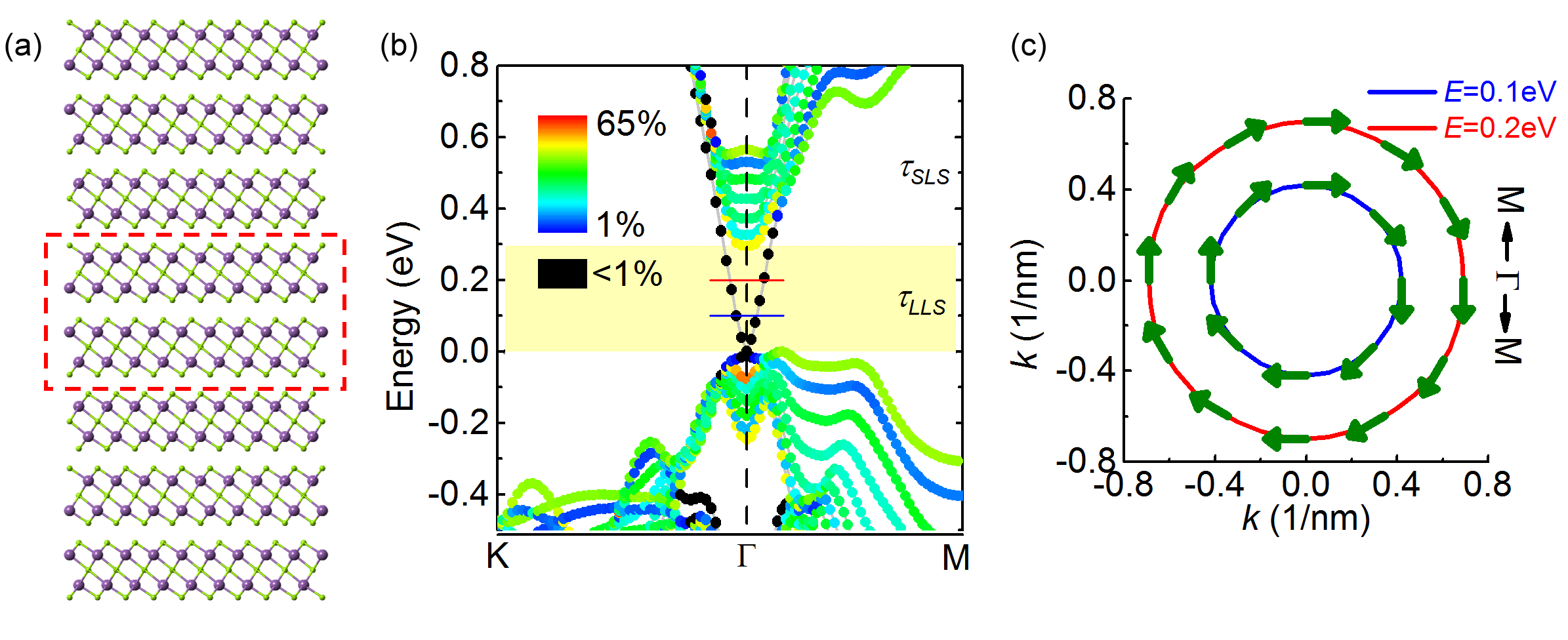
The electronic structure of the Bi2Se3 thin film of thickness QLs is shown in Fig. 1b, in which we can see the massless Dirac cone with the Dirac point at zero energy. The Dirac-cone states are doubly degenerate states, which can be regarded as two TSSs on different sides of the film. As can be seen, there is a bulk gap, the energy region between the valence band edge (VBE) meV and the conduction band edge (CBE) meV indicated by the yellow shaded region, in which there is no electronic states except for the TSSs. The wave functions of the TSSs on different sides of the film are spatially separated so that the orbital contribution from the atoms in the middle QLs (indicated by the red box in Fig. 1a) is less than . The TSSs in the bulk gap (hereafter call the LLSs) should have long relaxation times due to two reasons. (i) The large-angle scattering between the TSSs on the same side of the thin film is suppressed because the spin polarization of the TSSs circulates around the point as can be seen in Fig. 1c. (ii) The scattering between the TSSs on the opposite sides of the thin film is negligible because of the spatial separation between the initial and final states as mentioned above. The relaxation times of the other states (hereafter call the SLSs), , should be much smaller than that of the LLSs, , because the electrons of the SLSs can be elastically scattered into the bulk states. The long relaxation time of the TSSs in the bulk gap (i.e., the LLSs) can be demonstrated by comparing our computed value of the sheet conductance with the experimental data in ref. 37 (see Supplementary Information for more details). The estimated value is fs, which is about two orders higher than that of bulk relaxation time ( fs)Luo(2012) . In this paper, we adopt the dual relaxation time model, which is a generalization of the conventional constant relaxation time approximationZhangSC(2014) . In this model, the relaxation times and are two constants. The integral is divided into the LLS part and the SLS part . Then we can define the LLS (SLS) electrical conductance ( ), and the LLS (SLS) Seebeck coefficient ( ) by the equations the same as equations (2) and (3), except that the integral is replaced by the (). According to this definition, the electrical conductance is the sum of the LLS and the SLS conductancesGoldsmid(book) ,
| (9) |
On the other hand, the Seebeck coefficient is a weighted average of the Seebeck coefficients associated with the two type of the carriers,
| (10) |
III.2 Thermoelectric transport properties
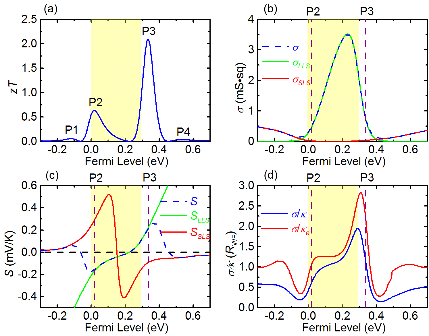
The room-temperature TE figure of merit of the QL Bi2Se3 film as a function of the Fermi level is shown in Fig. 2a. Here, the relaxation time of the LLSs and the SLSs are, respectively, set to be fs and fs. As can be seen, there are four peaks denoted by P1-P4, among which the P1 (P4) is located away from the VBE (CBE). When the Fermi level is near the P1 or P4 energy, the conduction carriers are almost the SLS carriers. On the other hand, the peak P2 (P3) is located near the VBE (CBE). When the Fermi level is around the P2 (P3) energy, both the LLSs and the SLSs are significant to the TE performance. The peak values of P2 and P3 are much greater than those of P1 and P4. Hereafter, we will mainly focus on P2 and P3. Sometimes, we may only discuss the case of P3, and the discussion of P2 is similar to that of P3 unless otherwise mentioned.
Figure 2b shows the electrical sheet conductance as a function of the Fermi level. As can be seen, when the Fermi level is located in the bulk gap, the magnitude of the total conductance is nearly equal to that of the LLS contribution. Because the LLS density of states (DOS) increases with the Fermi level, the conductance increases with the Fermi level to the maximum at the energy about (or 65 meV) below the CBE. It then decreases because of the decline in the conduction carrier number of the LLSs regardless the increase in that of the SLSs. When the Fermi level is at the P3 energy, which is meV above the CBE, the conduction carrier number of the SLSs is much larger than that of the LLSs. Nevertheless, the total conductance is mainly contributed from the LLS conductance because of the large relaxation time difference between the LLSs and the SLSs.
The Seebeck coefficient as a function of the Fermi level is shown in Fig. 2c. Similar to the typical semiconductor cases, the SLS Seebeck coefficient is negative for -type doping () and positive for -type doping ( ). When the Fermi level is in the bulk gap and away from the midgap, the magnitude of the increases as the Fermi level moves toward the midgap. This can be easily comprehended by rewriting the Seebeck coefficients of the LLSs and the SLSs as
| (11) |
where
| (12) |
is the TDF-weighted average energy of the conduction carriers, and () the energy region of the LLSs (SLSs), i.e. the yellow (white) shaded region in Figs. 1b and 2. For -type (-type) doping, almost all the conduction carriers and hence the are slight higher (lower) than the CBE (VBE) so that the magnitude of the increase as the Fermi level moves toward the midgap. Due to the bipolar effect, the magnitude of the reduces near the middle of the gapGoldsmid(book) . The LLS Seebeck coefficient generally has a sign opposite to the SLS Seebeck coefficient . The magnitude of the LLS Seebeck coefficient increases as the Fermi level moves away from the energy region of the LLSs. This can also be comprehended from equation (11) by considering the fact that the is located in the energy region . The energy of is higher than the midgap energy because the LLS DOS increases with energy. As defined in equation (10), the Seebeck coefficient is a conductance-weighted average of the LLS and the SLS Seebeck coefficients. In the limit , the Seebeck coefficient is nearly equal to LLS Seebeck coefficients, whose magnitude is extraordinarily large when the Fermi level is away from the energy region . In the present case, the relaxation time of the SLSs is indeed much smaller than that of the LLSs. The resultant magnitude of the Seebeck coefficient at P3 (P2) is nearly the same as magnitude of the and it is as large as () mV/K.
The ratio of the electrical conductance to the electronic thermal conductance as a function of the Fermi level is shown in Fig. 2d. It is normalized in unit of , which is the value given by the Wiedemann-Franz lawMermin(book) . As can be seen, the Wiedemann-Franz law is generally applicable (i.e., ) except for the energy around the band edges. The Wiedemann-Franz law can be derived by applying the Sommerfeld expansion on equation (5) and retaining the lowest non-vanishing orderMermin(book) . Because the relaxation time of the electrons near the band edge and the corresponding TDF vary rapidly with the energy, the higher-order terms are significant. By taking into account the higher-order terms and replacing with , the ratio can be approximated as
| (13) |
where the prime denotes the derivative with respect to . The first term is just the result of the Wiedemann-Franz law. In the energy region slightly below the CBE, the electrical conductance decreases rapidly with energy. The second term becomes significant, and the ratio increases with energy to a value much larger than . When the energy further increases, the dominant type of the conduction carriers changes from the LLS to the SLS and the sign of the changes from negative to positive. This leads to the decrease of the magnitude of the and a considerable positive . As a result, the ratio decreases with energy to a value smaller than . Because the magnitude of the Seebeck coefficient increases with energy, the peak P3 is always located at the energy region where the ratio decreases with energy. The ratio at P3 energy is more than twice larger than the value given by the Wiedemann-Franz law. Unlike the case of , the ratio shows no significant increase as . This is mainly because the energy of the Dirac point is nearly the same as that of the VBE. The LLS DOS near the VBE is much smaller than that near the CBE. Therefore, the variation of the TDF with energy near the VBE is not as significant as that near the CBE. This is also the reason why the figure of merit at P2 is smaller than that at P3 and why the P2 is located in the energy region while the P3 is in the .
III.3 Further Enhancement by shortening the SLS relaxation time
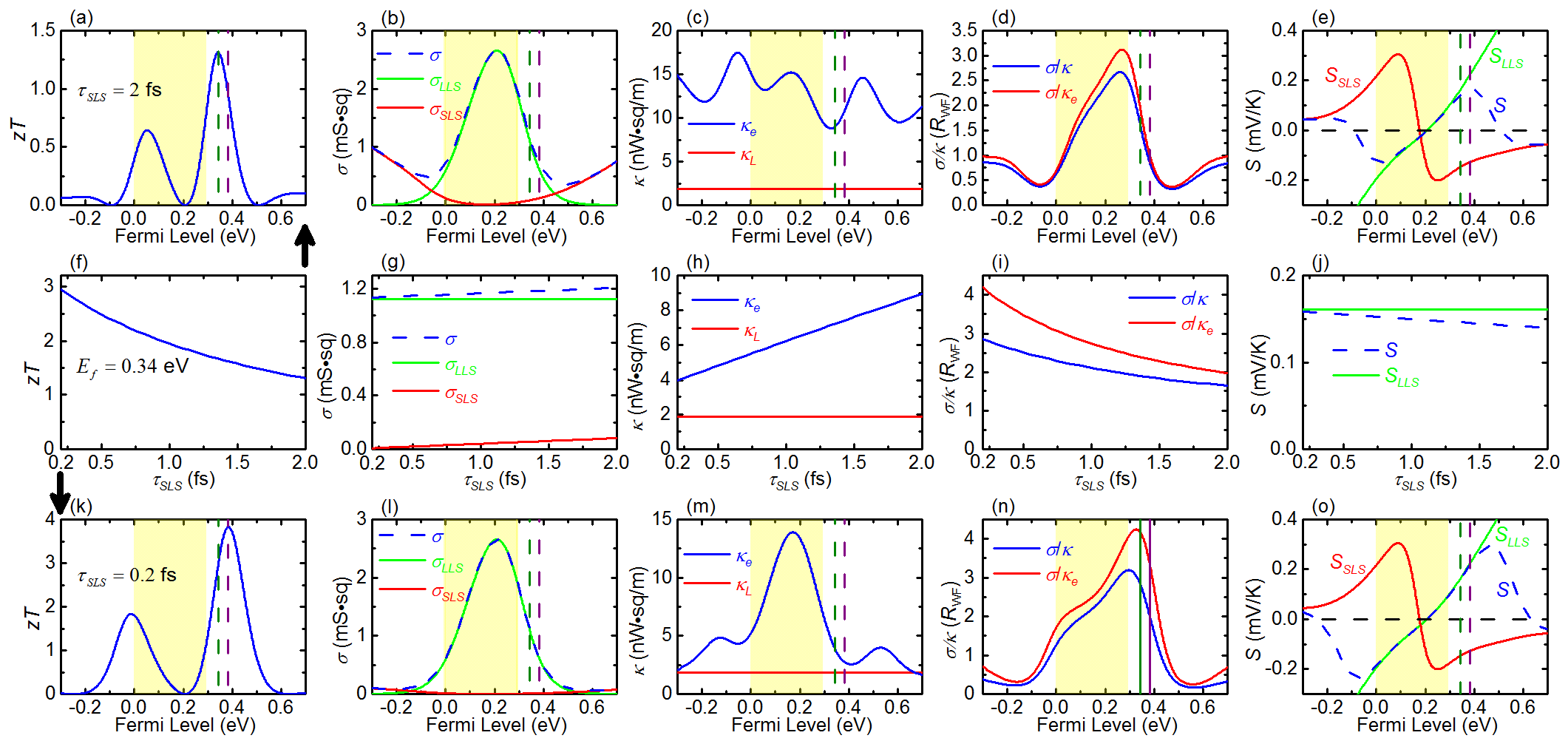
The TE performance can be further enhanced by reducing the SLS relaxation time. This can be done without changing the LLS relaxation time by introducing defects in the middle layers as mentioned earlier. As an example, we calculate the TE parameters at temperature K as shown in Fig. 3. Figure 3a-e shows the results of fs and Fig. 3k-o the results of fs. The TE parameters as functions of the SLS relaxation time in the range from to fs for eV (the P3 energy for fs) are shown in Fig. 3f-j. As can be seen in Fig. 3b and 3l, when the SLS relaxation time reduces from fs to fs, the SLS conductance becomes negligible around the P3 energy. This causes the increase (decrease) of the magnitude of (). The increase (decrease) of the magnitude of () leads to the increase of the ratio as shown in Fig. 3i. Furthermore, the magnitude of the Seebeck coefficient increases with the decreasing SLS relaxation time. It is nearly equal to the magnitude of LLS Seebeck coefficient when fs as shown in Fig. 3j. These cause the remarkable increase in the figure of merit at P3 energy from to (see Fig. 3f) in spite of the slight decrease of the electrical conductance (see Fig. 3g). The reduction of the SLS relaxation time results in the blue shift of the P3 energy as indicated by the blue and green dashed lines in Figs 3a, k. This further enhances the figure of merit to the value of . In addition, we perform similar calculation for the room temperature (see Fig. S3). We find the figure of merit is also significantly enhanced. It increases from to when the SLS relaxation time decreases from fs to fs.
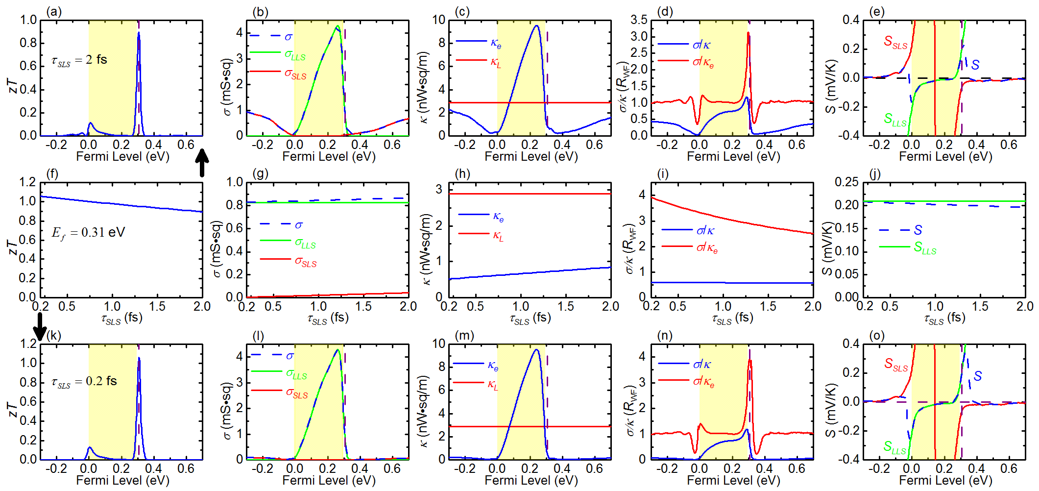
Figure 4 is a low-temperature ( K) counterpart of Fig. 3. As can be seen, the magnitude of the figure of merit only slightly increases from to when the SLS relaxation time reduces from fs to fs. In addition, it would be difficult to experimentally tune the Fermi level in such a narrow peak width ( eV) at low temperature as can be seen in Fig 3a, k. Unlike the high-temperature ( K) case, in which the electronic thermal conductance is generally much larger than the lattice thermal conductance as shown in Fig. 3c, h and m, the electronic thermal conductance at low temperature ( K) near the P3 energy is much smaller than the lattice thermal conductance as shown in Fig. 4c, h and m. Consequently, the ratio is nearly a constant even though the ratio increases significantly with the decrease of the SLS relaxation time as shown in Fig. 4i.
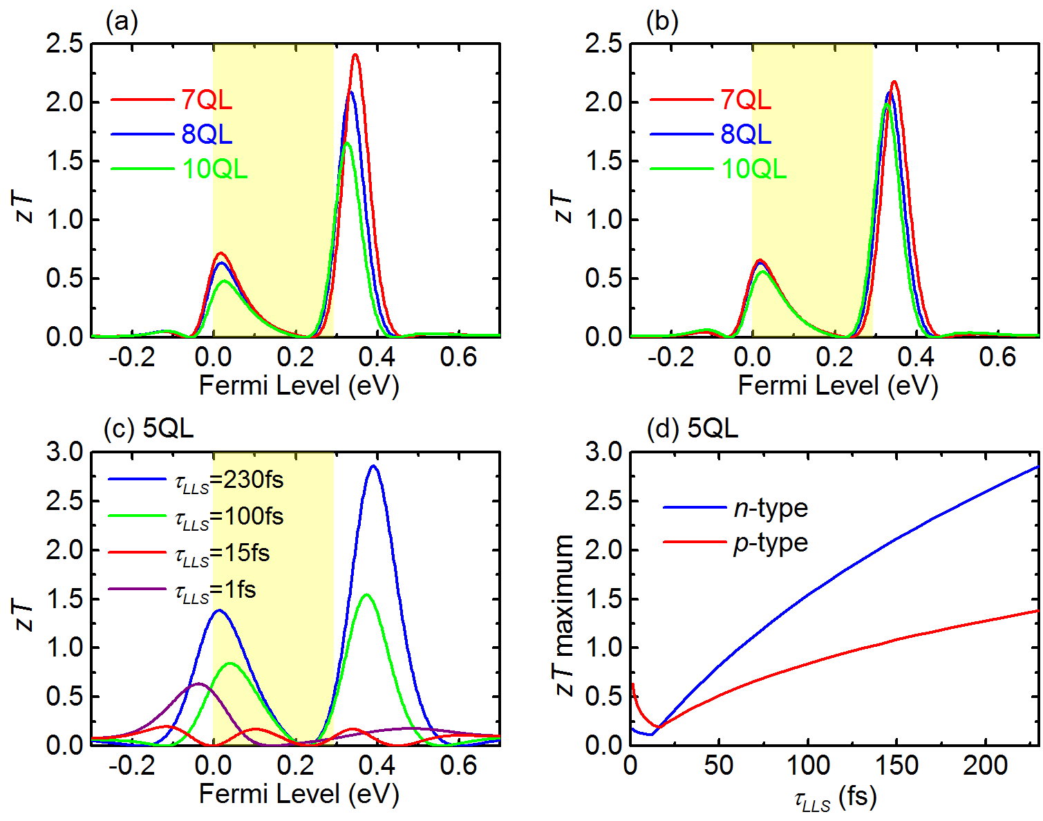
III.4 Thickness Dependence of the TE Performance
Figure 5a shows the figure of merit of the , and QL Bi2Se3 thin films at room temperatue. As can be seen, the figure of merit of P2 and P3 decreases with the film thickness. Figure 5b is the same as Fig. 5a except that the lattice thermal conductance of the QL and the QL films is set at the value the same as that of the QL film. We find the figure of merit difference between the films of different thickness is greatly reduced indicating that the decrease of the figure of merit with increasing thickness is mainly due to the increase of the lattice thermal conductance. As we mentioned earlier, the TE performance can be enhanced by introducing defects into the middle layers of the thin film so that the SLS relaxation time can be reduced without changing the LLS relaxation time. For the case of larger film thickness, the low SLS relaxation time should be more easily to achieve. However, the thermal conductance increases at the same time. As we discussed earlier, the figure of merit will barely increase with decreasing SLS relaxation time if the electronic thermal conductance is much smaller than the lattice thermal conductance . Therefore, the optimized film thickness should be the smallest thickness that the condition can be satisfied by introducing defects. In addition, it should not be smaller than QLs as discussed below.
Thus far, we consider the case of the film thickness larger than QLs. When the film thickness is smaller than QLs, the LLS relaxation time will be dramatically reduced by the scattering between the TSSs on the opposite sides as demonstrated in Supplementary Information. In this case, introducing defects into the Bi2Se3 thin film will significantly reduce not only the SLS relaxation time but also the LLS relaxation time . Figure 5c shows the figure of merit of the QL Bi2Se3 thin film for the LLS relaxation times shorter than fs in the case of the SLS relaxation time fs at temperature . The corresponding maximum for -type (-type) doping as a function of the LLS relaxation time is shown in Fig. 5d. Here, the -type (-type) doping is defined as the maximum in the case of the Fermi level higher (lower) than eV. As can be seen, the figure of merit generally decreases with decreasing LLS relaxation time. For -type doping, the maximum reduces from to when the LLS relaxation time decreases from fs to fs. When the LLS relaxation is reduced to about fs, the LLS conductance is comparable with the SLS conductance causing a strong cancelation between the LLS Seebeck coefficient and the SLS Seebeck coefficient as indicated by equation (10). The relatively small relaxation time ratio also deteriorates the TE performance by reducing the ratio of as indicated in equation (13). When the LLS relaxation time further decreases, the figure of merit at P4 (P1) is larger than that at P3 (P2). In this case, the maximum increases with decreasing because the bulk carriers dominate the transport when the Fermi level is at P4 (P1) energy. Finally, when the LLS relaxation time is reduced to fs (i.e., ), the P2 and P3 disappear, and only the P1 and P4 remain. The quite large maximum for -type doping is mainly due to the large DOS of the valence bands.
IV Conclusions
In summary, we investigate the TE properties of the Bi2Se3 thin film through the first-principle calculations and the Boltzmann transport theory. When the film thinness is so large ( QLs) that the coupling between the TSSs on the opposite sides of the film is negligible, the large-angle scattering is strongly suppressed, and the relaxation time of the LLSs can be hundreds of times larger than that of the SLSs as demonstrated by comparing our calculations with the earlier experimental data (see Supplementary Information). As a result, the reduction of the magnitude of the Seebeck coefficient near the P3 (P2) energy caused by the SLS carriers is negligible and the Seebeck coefficient is nearly equal to the LLS Seebeck coefficient. The ratio of the electrical conductance to the electronic thermal conductance can be dramatically deviated from the value given by the Wiedemann-Franz law when the Fermi level is near the band edges and much larger than when the Fermi level is at the P3 energy. The TE performance can be further enhanced by reducing the SLS relaxation time without changing LLS relaxation time. This enhancement is prominent especially at high temperature and achievable by introducing defects in the middle layers. When the film thickness increases to QLs, the figure of merit decreases mainly due to the increase of the thermal conductance. When the film thickness decreases to the thickness smaller than QLs, the TE performance will be greatly deteriorated because of the effective coupling between the TSSs on the opposite sides of the thin film. The optimized film thickness would be the smallest one, that can satisfy the condition by introducing defect in the region more than QLs away from the surface, and should be not smaller than QLs. Although we only consider the thin films made of Bi2Se3, the high TE performance caused by the coexistence of the LLS and SLS conduction carriers is expected in some of the other TI thin films.
Acknowledgement 1
This work was supported by the Ministry of Science and Technology, Taiwan.
References
- (1) Zevenhoven, R. & Beyene, A. The relative contribution of waste heat from power plants to global warming. Energy 36, 3754-3762 (2011).
- (2) Rowe, D. M. (ed.) CRC Handbook of thermoelectrics. (CRC Press, 1955).
- (3) Tritt, T. M. & Subramanian, M. A. Thermoelectric materials, phenomena, and applications: A bird’s eye view. Mrs Bull 31, 188-194 (2006).
- (4) Snyder, G. J. Small thermoelectric generators. Electrochem. Soc. Interface 17, 54 (2008).
- (5) Tritt, T. M. Thermoelectric phenomena, materials, and applications. Annu. Rev. Mater. Res. 41, 433-448 (2011).
- (6) Alam, H. & Ramakrishna, S. A review on the enhancement of figure of merit from bulk to nano-thermoelectric materials. Nano Energy 2, 190-212 (2013).
- (7) He, W., Zhang, G., Zhang, X. X., Ji, J., Li, G. Q. & Zhao, X. D. Recent development and application of thermoelectric generator and cooler. Appl. Energ. 143, 1-25 (2015).
- (8) Aswal, D. K., Basu, R. & Singh, A. Key issues in development of thermoelectric power generators: High figure-of-merit materials and their highly conducting interfaces with metallic interconnects. Energ. Convers. Manage. 114, 50-67 (2016).
- (9) Zhang, Q. H., Huang, X. Y., Bai, S. Q., Shi, X., Uher, C. & Chen, L. D. Thermoelectric devices for power generation: Recent progress and future challenges. Adv. Eng. Mater. 18, 194-213 (2016).
- (10) Kane, C. L. & Mele, E. J. Z(2) topological order and the quantum spin Hall effect. Phys. Rev. Lett. 95, 146802 (2005).
- (11) Bernevig, B. A. & Zhang, S. C. Quantum spin hall effect. Phys. Rev. Lett. 96, 106802 (2006).
- (12) Fu, L., Kane, C. L. & Mele, E. J. Topological insulators in three dimensions. Phys. Rev. Lett. 98, 106803 (2007).
- (13) Moore, J. E. & Balents, L. Topological invariants of time-reversal-invariant band structures. Phys. Rev. B 75, 121306 (2007).
- (14) Qi, X. L., Hughes, T. L. & Zhang, S. C. Topological field theory of time-reversal invariant insulators. Phys. Rev. B 78, 195424 (2008).
- (15) Hasan, M. Z. & Kane, C. L. Colloquium: Topological insulators. Rev. Mod. Phys. 82, 3045-3067 (2010).
- (16) Bansil, A., Lin, H. & Das, T. Colloquium: Topological band theory. Rev. Mod. Phys. 88 (2016).
- (17) Zhang, H. J., Liu, C. X., Qi, X. L., Dai, X., Fang, Z. & Zhang, S. C. Topological insulators in Bi2Se3, Bi2Te3 and Sb2Te3 with a single Dirac cone on the surface. Nat. Phys. 5, 438-442 (2009).
- (18) Chen, Y. L., Analytis, J. G., Chu, J. H., Liu, Z. K., Mo, S. K., Qi, X. L., Zhang, H. J., Lu, D. H., Dai, X., Fang, Z., Zhang, S. C., Fisher, I. R., Hussain, Z. & Shen, Z. X. Experimental realization of a three-dimensional topological insulator, Bi2Te3. Science 325, 178-181 (2009).
- (19) Xie, W. J., He, J., Kang, H. J., Tang, X. F., Zhu, S., Laver, M., Wang, S. Y., Copley, J. R. D., Brown, C. M., Zhang, Q. J. & Tritt, T. M. Identifying the specific nanostructures responsible for the high thermoelectric performance of (Bi,Sb)2Te3 nanocomposites. Nano Lett. 10, 3283-3289 (2010).
- (20) Muchler, L., Casper, F., Yan, B. H., Chadov, S. & Felser, C. Topological insulators and thermoelectric materials. Phys. Status Solidi-R 7, 91-100 (2013).
- (21) Shi, H. L., Parker, D., Du, M. H. & Singh, D. J. Connecting thermoelectric performance and topological-insulator behavior: Bi2Te3 and Bi2Te2Se from first principles. Phys. Rev. Appl. 3 (2015).
- (22) Xu, Y., Gan, Z. X. & Zhang, S. C. Enhanced thermoelectric performance and anomalous Seebeck effects in topological insulators. Phys. Rev. Lett. 112, 226801 (2014).
- (23) Liang, J. H., Cheng, L., Zhang, J., Liu, H. J. & Zhang, Z. Y. Maximizing the thermoelectric performance of topological insulator Bi2Te3 films in the few-quintuple layer regime. Nanoscale 8, 8863-8870 (2016).
- (24) Xia, Y., Qian, D., Hsieh, D., Wray, L., Pal, A., Lin, H., Bansil, A., Grauer, D., Hor, Y. S., Cava, R. J. & Hasan, M. Z. Observation of a large-gap topological-insulator class with a single Dirac cone on the surface. Nat. Phys. 5, 398-402 (2009).
- (25) Hsieh, D., Xia, Y., Qian, D., Wray, L., Dil, J. H., Meier, F., Osterwalder, J., Patthey, L., Checkelsky, J. G., Ong, N. P., Fedorov, A. V., Lin, H., Bansil, A., Grauer, D., Hor, Y. S., Cava, R. J. & Hasan, M. Z. A tunable topological insulator in the spin helical Dirac transport regime. Nature 460, 1101-1105 (2009).
- (26) Sun, Y. F., Cheng, H., Gao, S., Liu, Q. H., Sun, Z. H., Xiao, C., Wu, C. Z., Wei, S. P. & Xie, Y. Atomically thick bismuth selenide freestanding single layers achieving enhanced thermoelectric energy harvesting. J. Am. Chem. Soc. 134, 20294-20297 (2012).
- (27) Kresse, G. & Furthmuller, J. Efficiency of ab-initio total energy calculations for metals and semiconductors using a plane-wave basis set. Comp. Mater. Sci. 6, 15-50 (1996).
- (28) Kresse, G. Ab initio molecular dynamics for liquid-metals. J. Non-Cryst Solids 193, 222-229 (1995).
- (29) Kresse, G. & Furthmuller, J. Efficient iterative schemes for ab initio total-energy calculations using a plane-wave basis set. Phys. Rev. B 54, 11169-11186 (1996).
- (30) Perdew, J. P., Chevary, J. A., Vosko, S. H., Jackson, K. A., Pederson, M. R., Singh, D. J. & Fiolhais, C. Atoms, molecules, solids, and surfaces: Applications of the generalized gradient approximation for exchange and correlation. Phys. Rev. B 46, 6671-6687 (1992).
- (31) Perdew, J. P. & Wang, Y. Pair-Distribution Function and Its Coupling-Constant Average for the Spin-Polarized Electron-Gas. Phys. Rev. B 46, 12947-12954 (1992).
- (32) Grimme, S., Antony, J., Ehrlich, S. & Krieg, H. A consistent and accurate ab initio parametrization of density functional dispersion correction (DFT-D) for the 94 elements H-Pu. J. Chem. Phys. 132 (2010).
- (33) Grimme, S., Ehrlich, S. & Goerigk, L. Effect of the damping function in dispersion corrected density functional theory. J. Comput. Chem. 32, 1456-1465 (2011).
- (34) Mahan, G. D. & Sofo, J. O. The best thermoelectric. Proc. Natl. Acad. Sci. USA 93, 7436-7439 (1996).
- (35) Callaway, J. Model for lattice thermal conductivity at low temperatures. Phys. Rev. 113, 1046-1051 (1959).
- (36) Navratil, J., Horak, J., Plechacek, T., Kamba, S., Lost’ak, P., Dyck, J. S., Chen, W. & Uher, C. Conduction band splitting and transport properties of Bi2Se3. J. Solid State Chem. 177, 1704-1712 (2004).
- (37) Taskin, A. A., Sasaki, S., Segawa, K. & Ando, Y. Manifestation of topological protection in transport properties of epitaxial Bi2Se3 thin films. Phys. Rev. Lett. 109, 066803 (2012).
- (38) Luo, X., Sullivan, M. B. & Quek, S. Y. First-principles investigations of the atomic, electronic, and thermoelectric properties of equilibrium and strained Bi2Se3 and Bi2Te3 including van der Waals interactions. Phys. Rev. B 86, 184111 (2012).
- (39) Goldsmid, H. J. Introduction to thermoelectricity. Vol. 121 (Springer, 2009).
- (40) Aschcroft, N. W. & Mermin, N. D. Solid state physics. (Holt-Saunders, 1976).