Dephasing in strongly anisotropic black phosphorus
Abstract
Weak localization was observed in a black phosphorus (bP) field-effect transistor 65 thick. The weak localization behaviour was found to be in excellent agreement with the Hikami-Larkin-Nagaoka model for fields up to 1 T, from which characteristic scattering lengths could be inferred. The dephasing length was found to increase linearly with increasing hole density attaining a maximum value of at a hole density of approximately inferred from the Hall effect. The temperature dependence of was also investigated and above 1 K, it was found to decrease weaker than the dependence characteristic of electron-electron scattering in the presence of elastic scattering in two dimensions. Rather, the observed power law was found to be close to that observed previously in other quasi-one-dimensional systems such as metallic nanowires and carbon nanotubes. We attribute our result to the crystal structure of bP which host a ‘puckered’ honeycomb lattice forming a strongly anisotropic medium for localization.
The recent surge of interest in the field of 2D atomic crystals has led to a number of important advances in our understanding of solid-state physics in two dimensions. These include transition metal dichalcogenides, topological insulators such as bismuth selenide, and phosphorene. For the latter, its underlying crystal structure inherited from black phosphorus (bP) is a ‘puckered’ honeycomb lattice hosting one-dimensional chains of atoms displaced out of the atomic plane of the honeycomb lattice, and running along the zig zag axis. Few-layer black phosphorus has been the subject of recent investigations wherein strong anisotropy was observed in electronic transport, optical absorption, thermal conductivity and angle-resolved photoemission measurements Xia et al. (2014); Wang et al. (2015); Luo et al. (2015); Kim et al. (2015). Here, we have studied the weak localization in a bP field-effect transistor and we found that the phase coherence length decays with temperature at a slower rate than that expected for a two-dimensional material. This more robust coherence is reminiscent to that previously reported in quasi-one-dimensional systems such as nanotubesAppenzeller et al. (2001) and metallic nanowiresNatelson et al. (2001). Our experimental study of weak localization in bP is amongst very few investigations of weak localization in strongly anisotropic media.
Unlike semi-metallic graphene, bP is a direct gap semiconductor Keyes (1953); Morita (1986). The bandgap is 0.3 eV in bulk and increases by quantum confinement to 1-2 eV in the monolayer limit Du et al. (2010); Das et al. (2014); Liang et al. (2014), ideal for applications in electronics and optoelectronics Castellanos-Gomez (2015). Black phosphorus field effect transistors (FETs) have been demonstrated by various groups Li et al. (2014); Xia et al. (2014); Liu et al. (2014); Koenig et al. (2014); Castellanos-Gomez et al. (2014); Wood et al. (2014), with hole field effect mobilities reaching up to and current modulation at room temperature Chen et al. (2015). In the presence of a large magnetic field normal to the bP atomic layers, Shubnikov-de Haas oscillations have been observed in bP FETs Li et al. (2016); Tayari et al. (2015); Chen et al. (2015); Gillgren et al. (2015).
Magnetotransport in the presence of a weak magnetic field normal to the bP atomic layers is less well studied. In a disordered 2-D system, coherent backscattering of charge carriers gives rise to a peak in the magnetoresistance known as weak localization (WL), see Bergmann (1984) for a review. Previous work on weak localization in 2D crystals has focused primarily on graphene Morozov et al. (2006); Wu et al. (2007); Tikhonenko et al. (2008) and has also been observed recently in molybdenum disulfide, revealing a phase coherence length of at that decays with increasing temperature as Neal et al. (2013), characteristic of electron-electron interactions in 2D. Dimensionality plays an important role in weak localization. Previous work in metal and semiconducting mesoscopic structures has shown the dephasing length exponent to decrease from to a value close to as the system geometry was reduced towards the one dimensional limit Natelson et al. (2001), in agreement with theory of weak localization Altshuler et al. (1982). Here, we have observed weak localization in a 65 nm thick bP FET whose dephasing length exponent is found to be suppressed, and closer to a value of 1/3. We attribute this weak localization behaviour to the anisotropic nature of the puckered bP atomic crystal structure whose holes dispersion is distinct along the hard (along) and easy (against) axis of the puckers, see Fig.1.
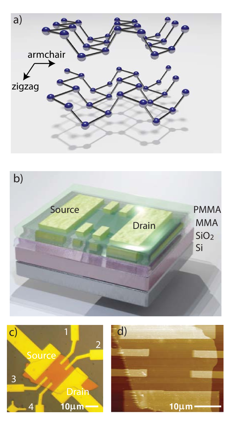
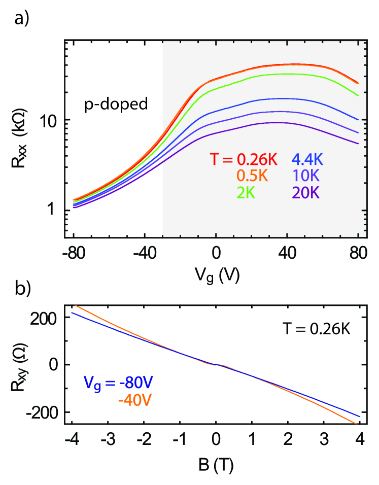
The design, as well as photograph and atomic force microscope images of the bP FET are shown in Fig.1. The longitudinal resistance versus back gate voltage is plotted in Fig. 2(a), with sample temperature as a parameter. The sample is highly resistive for , and exhibits clear p-type conduction for . The Hall resistance versus magnetic field is plotted in Fig. 2(b) at and at gate voltage and , with the component symmetric in removed. Hole carrier density inferred from the Hall resistance is found to depend linearly on gate voltage over the range of p-type conduction with a density of approximately cm2 at V. The field-effect hole mobility, was found to reach a peak value of at a gate voltage , with a negligible dependence upon temperature over the measured range .
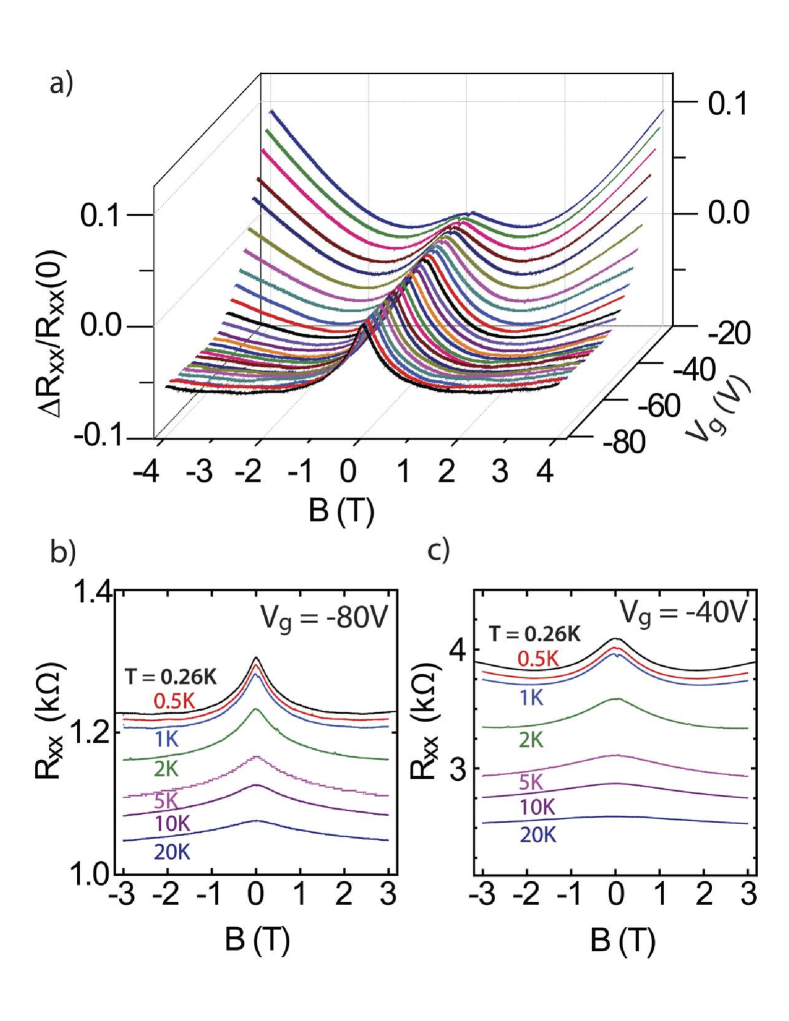
The measured weak localization peak in longitudinal resistance is shown in the plot of versus magnetic field and gate voltage in Fig. 3(a). The amplitude of the WL peak increases with increasing hole density attaining a maximum value at the highest negative gate voltage used in this experiment, -80V. The temperature dependence of the WL peak at and is plotted in Fig. 3(b) and Fig. 3(c), respectively. The WL correction to the resistance decreases with increasing temperature eventually disappearing at temperatures above 20 K, as expected.
The Hikami-Larkin-Nagaoka (HLN) theory Hikami et al. (1980); Maekawa and Fukuyama (1981); Bergmann (1984) gives a quantitative prediction for the WL correction to the sheet conductance,
| (1) | |||||
where is the digamma function. The field parameters in the above expression are given by:
| (2) | |||||
| (3) | |||||
| (4) |
where , , , and are the characteristic fields associated with elastic scattering, spin-orbit scattering, magnetic scattering, and inelastic scattering (dephasing), respectively.
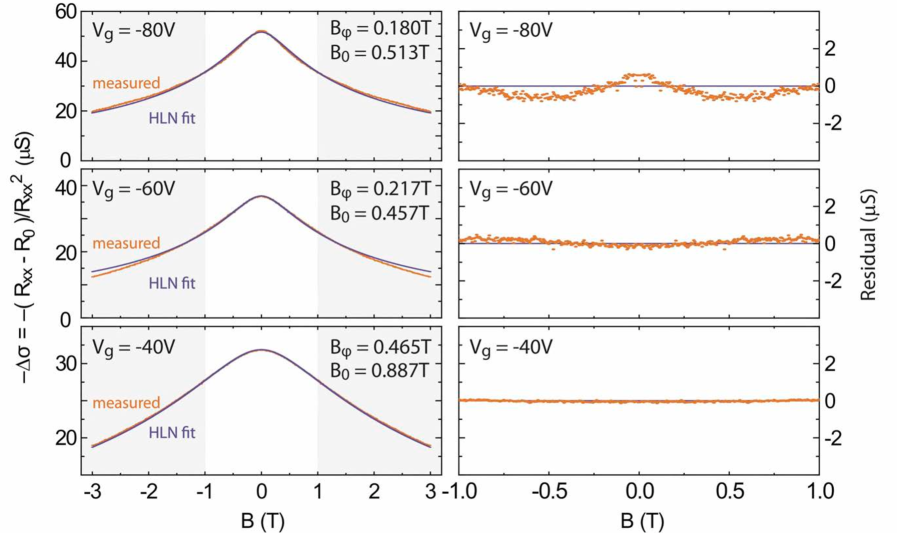
The measured WL peak (normalized) resistances were inverted into conductivity by the usual tensor relation , with negligible contributions from the (transverse) Hall resistivity (see 2(b)). To account for the background resistivity, the relation was used, where is the classical Drude resistance in the absence of a WL correction. The determination of the is not trivial, and was thus left as a fit parameter, however it was verified that its trend in temperature followed that of the measured transport mobility of the bP. This WL correction to conductivity was numerically fitted to the HLN model under the approximation of negligible spin-orbit coupling, , and negligible magnetic impurity scattering, . Both approximations are appropriate for our bP crystals ICP . Measurements and numerical fits of the WL contribution to conductivity are plotted in Fig. 4 versus backgate voltage at temperature K. The fit was performed over the magnetic field range , where the WL feature dominates the magnetoresistance. The fit quality was evaluated over the same -range, with an coefficient of determination of at minimum 0.99. The residuals are also shown in the right panels of Fig. 4.
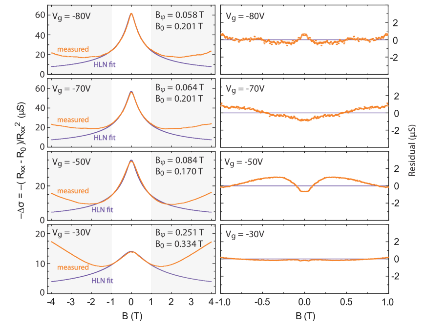
The extracted characteristic fields are related to the scattering lengths by considering the phase shift of diffusing charge carriers under the influence of a magnetic field, . From these fields, we can deduce elastic as well as inelastic (dephasing) characteristic lengths, and respectively. These lengths are plotted versus gate voltage in Fig. 5(a) at . In particular, the dephasing length clearly increases with increasing hole density, reaching a maximum of 55 nm, whereas remains nearly independent over a broad range of carrier density. We have also verified that scales linearly with the transport mobility, as expected for an elastic scattering process occurring in the presence of both a phonon bath and disorder.
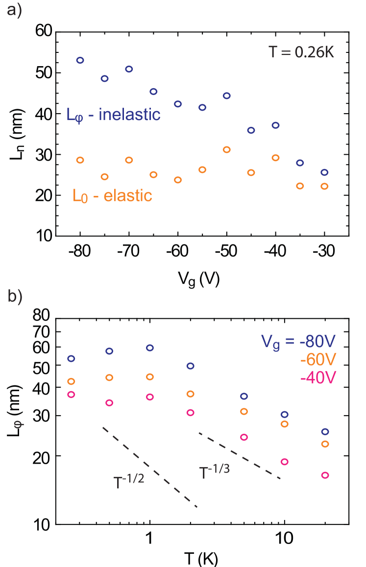
For weak localization occurring in typical disordered two-dimensional systems, the dephasing length is related to the inelastic scattering time via , where is the elastic diffusion coefficient. Electron-electron scattering in the absence of elastic scattering is expected to give a scattering rate , and hence Tikhonenko et al. (2009). In the diffusive transport regime, appropriate here since , the electron-electron scattering rate is expected to follow Altshuler et al. (1980); Abrahams et al. (1982); Altshuler et al. (1982), and hence . This characteristic inelastic scattering rate has been observed in graphene Morozov et al. (2006); Wu et al. (2007); Tikhonenko et al. (2008, 2009) and MoS2 Neal et al. (2013), however our weak localization measurements in a bP thin film clearly de not follow this trend. The temperature dependence of is shown in Fig. 5(b) in a log-log plot at fixed gate voltages . The experimental error in was determined by way of visual inspection of the quality of the fit when varying one parameter and keeping all others constant, and are contained within the size of the symbols. The saturation of at temperatures below 1 K is most likely due to impurities, as previously observed in a variety of metallic and semiconducting 2D systems Lin and Bird (2002). However, above 1 K the temperature dependence of does not follow the (dashed line) behaviour expected a priori from electron-electron scattering in the presence of elastic scattering in 2D. A weighted fit of the inelastic scattering length versus temperature rather show a suppressed dephasing length exponent (and corresponding 95% confidence interval withing bracket) of , with coefficients all greater than 0.99 at gate voltages , respectively.
Our WL mesurements reveal the presence of an inelastic scattering mechanism that is characterized by a decay in dephasing length weaker than . This is in contrast with previous measurements in a few-layer bP films Du et al. (2016) where a power law was also deduced, albeit with saturation of at higher temperatures than observed here (5 K as opposed to 1 K in our case). The analysis of Du et al. (2016) included a fitting parameter for valley degeneracy in bP. This parameter was found to differ from unity (no valley degeneracy) and to vary from 1.2 to 0.3 over the range of temperatures where the power law exponent for was extracted. The band structure of bP has been shown by photoemission studies Li et al. (2014), magnetotransportTayari et al. (2015), and density functional theoryQiao et al. (2014) to be absent of any valley degeneracies, calling into question the robustness of the scaling reported in Ref.Du et al. (2016).
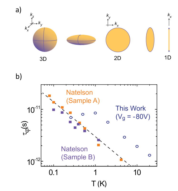
A weaker loss of the dephasing length with temperature, as compared to the 2D case, has previously been observed in the presence of a strong 1D confinement potential, e.g. in carbon nanotubes Appenzeller et al. (2001), and was shown to be well described by the theoretical prediction of a power law. Remarkably, the transition from the 2D limit to the quasi 1D limit was observed in the systematic study undertaken by Natelson et al.Natelson et al. (2001) whereby the dephasing time in metallic nanowires was measured as a function of the wire width down to 5 nm. In this regime of width and low temperatures, several heuristic length scales can be estimated placing the wires well into a quasi-1D regime. In this study a lower saturation temperature was observed, however the dephasing time was determined to follow closely a power law, corresponding to a dephasing length exponent . Fig.6 shows a comparison between Natelson’s dephasing time and the dephasing time of our bP FET at V. The expected power law for in the quasi-1D limit is also shown as a dotted line.
The robustness against dephasing in bP, when compared to the ideal 2D case in the presence of electron-electron scattering, is a priori unexpected. Years of previous work have shown weak localization (and hence dephasing) to be sensitive to system’s dimensionality. To our knowledge, there are two known scenarios for which a power-law exponent weaker than from can occur. These are i) strong confinement due to a 1D potential, as mentioned above and ii) dephasing by edge domain granularity Beliayev et al. . The crystalline order in our bP FET was carefully investigated by way of both unpolarized and polarized micro-Raman measurements and these data strongly suggest the bP flake to be an homogeneous single crystal (see supplementary information) rendering the granularity scenario unlikely. It is therefore more likely that the anisotropic nature of bP arising from puckers in the atomic plane which give rise to a an ellipsoid Fermi surface with heavy hole mass in the zig zag direction parallel with the puckers, and light hole mass in the armchair direction perpendicular to the puckers. Making use of calculated values for the effective masses as reported in Ref.Qiao et al. (2014), we estimate the corresponding Fermi wavelengths along and against the puckers to be and nm, respectively, at least one order of magnitude larger than any atomic lengthscales. In the basal direction, the presence of an electric field from the backgate has been shown to create a two-dimensional hole gas with a thickness of nm Li et al. (2016); Tayari et al. (2015), a scale that is much less than the thermal length nm over all temperaturea investigated in our experiment. These lengthscales place the bP FET into a strongly anisotropic regime for which weak, and even strong localization, has not yet been well studied.
The measured weak localization demonstrates a more robust coherence observed as a function of temperature as previously observed in quasi-one-dimensional systems such as nanotubes and metallic nanowires. Since it is highly sensitive to dimensionality, we attributed the more robust character of in bP to the highly anisotropic nature of the puckered honeycomb crystal structure. In the future, it will be of great interest to understand exactly how dephasing is affected by strong anisotropy in post-graphene 2D atomic crystals, a subject that is currently nearly free of any theoretical knowledge.
We thank Vincenzo Piazza for his help with the polarized Raman measurements. The authors thanks NSERC (Canada), Cifar (Canada), the Canada Research Chairs Program, Hydro-Québec, FRQNT (Québec) and the Institut de l’Energie Trottier for support. We also thank the European Research Council (ERC) under the European Union’s Horizon 2020 research and innovation program (Grant Agreement No. 670173) for funding the project PHOSFUN ‘Phosphorene functionalization: a new platform for advanced multifunctional materials’ through an ERC Advanced Grant. We acknowledge funding from the Italian Ministry of Foreign Affairs, Direzione Generale per la Promozione del Sistema Paese (agreements on scientific collaboration with Canada (Quebec) and Poland). Financial support from the CNR in the framework of the agreements on scientific collaboration between CNR and NRF (Korea), CNRS (France), and RFBR (Russia) is acknowledged. Furthermore, funding from the European Union Seventh Framework Programme under Grant Agreement No. 604391 Graphene Flagship is acknowledged. G.G. acknowledges two short-term mobility grants from CNR.
Special Note: upon the completion of this work and posting on the arXiv, we have become aware of similar results obtained by the UC Riverside group (Lau), arXiv:1608.00323.
Supplementary material for “Dephasing in strongly anisotropic black phosphorus”
Methods
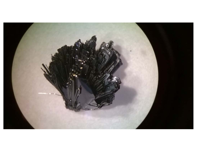
Our bP FETs were prepared by mechanical exfoliation of bulk bP crystals onto a degenerately doped Si wafer with a SiO2 layer prepared by dry thermal oxidation. The bP crystals were prepared by heating commercially available red phosphorus () in a muffle oven, together with a tin (), gold (), and a catalytic amount of SnI4, following a published procedure Nilges et al. (2008). The solids were loaded in a quartz tube, which was then evacuated by a pumping procedure where the vacuum was backfilled by gas several times and then the tube sealed under vacuum. Then, it was heated to to C (at a rate of C/min), kept 2h at this temperature and then heated up to 650ºC (C/min). The sample stayed for three days at this temperature in the oven. Afterwards, a slow cooling rate was chosen (C/min) to afford the formation of crystals of bP (typical size: 2 mm 3 mm). A photograph of a typical crystal is shown in the supplementary information. Exfoliation was performed in a nitrogen glove box to suppress photo-oxidation, and the SiO2 surface was treated with a hexamethyldisilazane (HMDS) layer to suppress charge transfer doping. Standard electron beam lithography was used to define 5 nm Ti/ 80 nm Au metal electrodes in a Hall bar geometry. The samples were made environmentally stable by encapsulation with of methyl methacrylate (MMA) and of polymethyl methacrylate (PMMA). The thickness of the bP was determined to be nm by AFM. Importantly, the hole accumulation layer induced in a bP FET at cryogenic temperatures is estimated to be thick, corresponding to a hole gas occupying 5-6 bP layers Tayari et al. (2016). Charge transport measurements were performed using standard ac lock-in techniques in a 3He cryostat with sample temperature ranging from K to K. A ac current at frequency Hz was applied through the source and drain terminals of the bP FET and both the longitudinal and transverse (Hall) voltages were measured. A dc gate voltage was applied to tune the carrier density through the back gate capacitance .
Unpolarized Raman Characterization
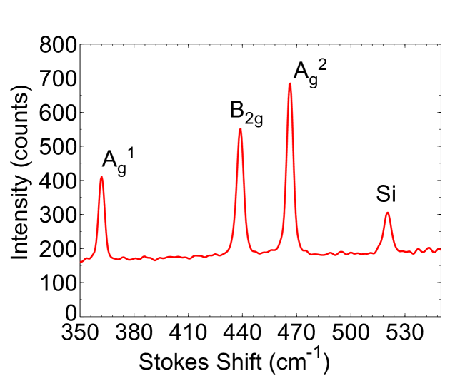
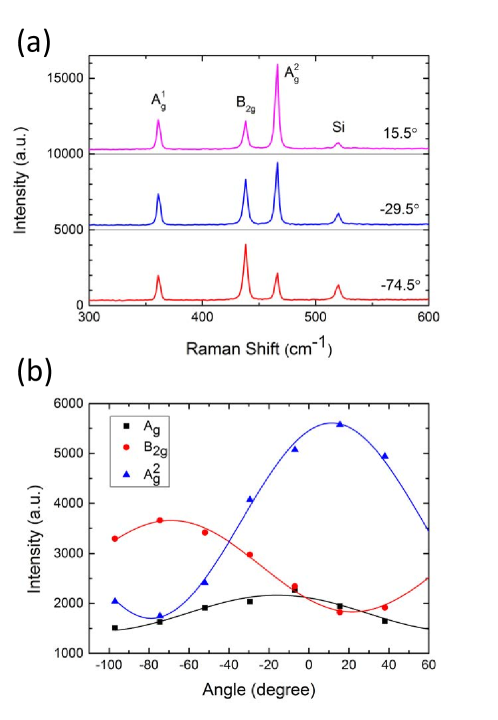
The Raman Stokes spectrum of the bP sample was measured after encapsulation by a 6 nm thick layer of gold for long term storage. Spectra were acquired with a micro-Raman spectrometer with a 532 nm laser pump and 5 mW of incident power to enable acquisition through the semi-transparent gold layer. A representative spectrum is shown in Fig.8. A silicon substrate peak at 520 cm-1 is observed, along with the A, B2g and A peaks characteristic of bP at 362 cm-1, 439 cm-1, and 466.5 cm-1, respectively. A red-shift of 3-7 cm-1 compared to our previous measurements of the Stokes peaks of bP at 369 cm-1, 443 cm-1, and 469.2 cm-1 Tayari et al. (2015), is likely originating from heating due to the elevated pump power required to acquire Raman spectra from gold encapsulated bP.
Polarized Raman Characterization
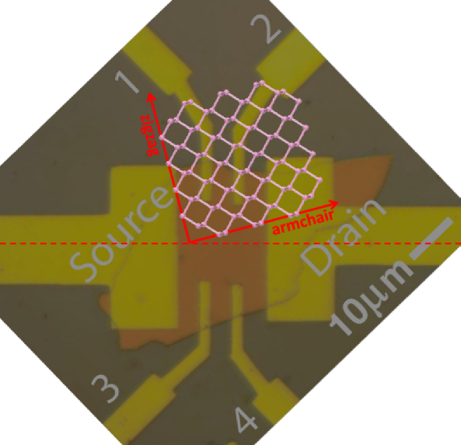
Polarized Raman spectroscopy was performed using a Renishaw inVia system equipped with a 532 nm laser, a half-wavelength retarder (half-wave plate), and a motorized stage for 2D mapping of samples. A laser spot size of approximately in diameter was used. Figure 9 a) shows three different spectra measured at different polarization angle with respect to the source-drain direction. At 0∘, the laser is polarized along the source-drain direction. Figure 9 b) shows the variation of the Raman peak intensities with polarization angle. The maximum of the peak is known to be along the armchair direction Sugai and Shirotani (1985); Wang et al. (2015), and it was deduced that the bP flake is oriented with an angle of approximately 15∘ with respect to the source-drain direction. A photograph of the device is shown in Fig.11 showing the cystal orientation with respect to the source-drain axis of the current leads.
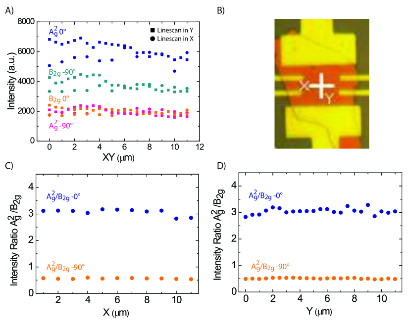
Subsequently, micro Raman measurements were performed to probe the homogeneity of the bP flake. In Fig.10 , the intensities of the and peaks are shown as a function of the position on the sample for incident laser polarizations of (i.e. source-drain direction) and (i.e. perpendicular to source-drain direction). The axis convention is shown in Fig.10 b). These two peaks were selected since their modulation with polarization angle was strongest. In panels c) and d) of Fig.10, the ratio is displayed for the two different polarization directions along the X and Y direction, respectively. The constant intensity ratio observed for a given polarization angle is strong indication that the bP flake is a single crystal.
Additional weak localization measurements and HLN fits
For completeness, additional data taken at 10K are shown in Fig.12 together with the HLN fits and residuals. The fitting procedure and the legend convention of the figure is identical to that described in the main text.
References
- Xia et al. (2014) F. Xia, H. Wang, and Y. Jia, Nat. Commun. 5, 4458 (2014).
- Wang et al. (2015) X. Wang, A. M. Jones, K. L. Seyler, V. Tran, Y. Jia, H. Zhao, H. Wang, L. Yang, X. Xu, and F. Xia, Nat. nanotech. 10, 517 (2015).
- Luo et al. (2015) Z. Luo, J. Maessen, Y. Deng, Y. Du, R. P. Garrelts, M. S. Lundstrom, P. D. Ye, and X. Xu, Nature communications 6, 8572 (2015).
- Kim et al. (2015) J. Kim, S. S. Baik, S. H. Ryu, Y. Sohn, S. Park, B. Park, J. Dendinger, Y. Yi, H. J. Choi, and K. S. Kim, Science 349, 6249 (2015).
- Appenzeller et al. (2001) J. Appenzeller, R. Martel, P. Avouris, H. Stahl, U. Hunger, and B. Lengeler, Phys. Rev. B 64, 121404(R) (2001).
- Natelson et al. (2001) D. Natelson, R. Willett, K. West, and L. Pfeiffer, Phys. Rev. Lett. 86, 1821 (2001).
- Keyes (1953) R. W. Keyes, Phys. Rev. 92, 580 (1953).
- Morita (1986) A. Morita, Appl. Phys. A 39, 227 (1986).
- Du et al. (2010) Y. Du, C. Ouyang, S. Shi, and M. Lei, J. Appl. Phys. 107, 093718 (2010).
- Das et al. (2014) S. Das, W. Zhang, M. Demarteau, A. Hoffmann, M. Dubey, and A. Roelofs, Nano Lett. 14, 5733 (2014).
- Liang et al. (2014) L. Liang, J. Wang, W. Lin, B. G. Sumpter, V. Meunier, and M. Pan, Nano Lett. 14, 6400 (2014).
- Castellanos-Gomez (2015) A. Castellanos-Gomez, J. Phys. Chem. Lett. 6, 4280 (2015).
- Li et al. (2014) L. Li, Y. Yu, G. J. Ye, Q. Ge, X. Ou, H. Wu, D. Feng, X. H. Chen, and Y. Zhang, Nat. Nanotechnol. 9, 372 (2014).
- Liu et al. (2014) H. Liu, A. T. Neal, Z. Zhu, Z. Luo, X. Xu, D. Tomanek, and P. D. Ye, ACS Nano 8, 4033 (2014).
- Koenig et al. (2014) S. P. Koenig, R. A. Doganov, H. Schmidt, A. H. Castro Neto, and B. Ozyilmaz, Appl. Phys. Lett. 104, 103106 (2014).
- Castellanos-Gomez et al. (2014) A. Castellanos-Gomez, L. Vicarelli, E. Prada, J. O. Island, K. L. Narasimha-Acharya, S. I. Blanter, D. J. Groenendijk, M. Buscema, G. A. Steele, J. V. Alvarez, H. W. Zandbergen, J. J. Palacios, and H. S. J. van der Zant, 2D Materials 1, 025001 (2014).
- Wood et al. (2014) J. D. Wood, S. A. Wells, D. Jariwala, K.-S. Chen, E. Cho, V. K. Sangwan, X. Liu, L. J. Lauhon, T. J. Marks, and M. C. Hersam, Nano Lett. 14, 6964 (2014).
- Chen et al. (2015) X. Chen, Y. Wu, Z. Wu, Y. Han, S. Xu, L. Wang, W. Ye, T. Han, Y. He, Y. Cai, and N. Wang, Nat. Comm. 6, 7315 (2015).
- Li et al. (2016) L. Li, G. J. Ye, V. Tran, R. Fei, G. Chen, H. Wang, J. Wang, K. Watanabe, T. Taniguchi, L. Yang, X. H. Chen, and Y. Zhang, Nat. Nanotech. 10, 41 (2016).
- Tayari et al. (2015) V. Tayari, N. Hemsworth, I. Fakih, A. Favron, E. Gaufres, G. Gervais, R. Martel, and T. Szkopek, Nat. Comm. 6, 7702 (2015).
- Gillgren et al. (2015) N. Gillgren, D. Wickramaratne, Y. Shi, T. Espiritu, J. Yang, J. Hu, J. Wei, X. Liu, Z. Mao, K. Watanabe, T. Taniguchi, M. Bockrath, Y. Barlas, R. K. Lake, and C. N. Lau, 2D Mater. 2, 011001 (2015).
- Bergmann (1984) G. Bergmann, Physics Reports 107, 1 (1984).
- Morozov et al. (2006) S. V. Morozov, K. S. Novoselov, M. I. Katsnelson, F. Schedin, L. A. Ponomarenko, D. Jiang, and A. K. Geim, Phys. Rev. Lett. 97, 016801 (2006).
- Wu et al. (2007) X. Wu, X. Li, Z. Song, C. Berger, and W. A. de Heer, Phys. Rev. Lett. 98, 136801 (2007).
- Tikhonenko et al. (2008) F. V. Tikhonenko, D. W. Horsell, R. V. Gorbachev, and A. K. Savchenko, Phys. Rev. Lett. 100, 056802 (2008).
- Neal et al. (2013) A. T. Neal, H. Liu, J. Gu, and P. D. Ye, ACS Nano 7, 7077 (2013).
- Altshuler et al. (1982) B. L. Altshuler, A. G. Aronov, and D. E. Khmelnitsky, J. Phys. C: Solid State Phys. 15, 7367 (1982).
- Hikami et al. (1980) S. Hikami, A. I. Larkin, and Y. Nagaoka, Progress of Theoretical Physics 63, 707 (1980).
- Maekawa and Fukuyama (1981) S. Maekawa and H. Fukuyama, J. Phys. Soc. Jpn. 50, 2516 (1981).
- (30) We have performed an analysis of the bP crystal used in these experiments by Inductively Coupled Plasma-Mass Spectrometry (ICP-MS) which revealed a negligible level of magnetic and heavy elements, below 1 . In addition, phosphorus being a light element, its spin orbit coupling is negligeably small.
- Tikhonenko et al. (2009) F. V. Tikhonenko, A. A. Kozikov, A. K. Savchenko, and R. V. Gorbachev, Phys. Rev. Lett. 103, 226801 (2009).
- Altshuler et al. (1980) B. L. Altshuler, D. Khmelnitzkii, A. I. Larkin, and P. A. Lee, Phys. Rev. B 22, 5142 (1980).
- Abrahams et al. (1982) E. Abrahams, P. W. Anderson, P. A. Lee, and T. V. Ramakrishnan, Phys. Rev. B 24, 6783 (1982).
- Lin and Bird (2002) J. J. Lin and J. P. Bird, J. Phys. Cond. Matter 14, R501 (2002).
- Du et al. (2016) Y. Du, A. T. Neal, H. Zhou, and P. D. Ye, 2D Materials 3, 024003 (2016).
- Qiao et al. (2014) J. Qiao, X. Kong, Z.-H. Hu, and W. Ji, Nature communications 5, 4475 (2014).
- (37) E. Beliayev, B. Beletsev, and Y. Kolesnichenko, Low Temperature Physics, year = 2011, volume = 37, pages = 318, owner = Moi, .
- Nilges et al. (2008) T. Nilges, M. Kersting, and T. Pfeifer, J. of Solid State Chem. 181, 1707 (2008).
- Tayari et al. (2016) V. Tayari, N. Hemsworth, O. Cyr-Choinière, W. Dickerson, G. Gervais, and T. Szkopek, Phys. Rev. Applied 5, 064004 (2016).
- Sugai and Shirotani (1985) S. Sugai and Shirotani, Solid State Comm. 53, 753 (1985).