Theory of proximity-induced exchange coupling in graphene on hBN/(Co, Ni)
Abstract
Graphene, being essentially a surface, can borrow some properties of an insulating substrate (such as exchange or spin-orbit couplings) while still preserving a great degree of autonomy of its electronic structure. Such derived properties are commonly labeled as proximity. Here we perform systematic first-principles calculations of the proximity exchange coupling, induced by cobalt (Co) and nickel (Ni) in graphene, via a few (up to three) layers of hexagonal boron nitride (hBN). We find that the induced spin splitting of the graphene bands is of the order of 10 meV for a monolayer of hBN, decreasing in magnitude but alternating in sign by adding each new insulating layer. We find that the proximity exchange can be giant if there is a resonant level of the transition metal close to the Dirac point. Our calculations suggest that this effect could be present in Co heterostructures, in which a level strongly hybridizes with the valence-band orbitals of graphene. Since this hybridization is spin dependent, the proximity spin splitting is unusually large, about 10 meV even for two layers of hBN. An external electric field can change the offset of the graphene and transition-metal orbitals and can lead to a reversal of the sign of the exchange parameter. This we predict to happen for the case of two monolayers of hBN, enabling electrical control of proximity spin polarization (but also spin injection) in graphene/hBN/Co structures. Nickel-based heterostructures show weaker proximity effects than cobalt heterostructures. We introduce two phenomenological models to describe the first-principles data. The minimal model comprises the graphene (effective) orbitals and can be used to study transport in graphene with proximity exchange, while the - model also includes hybridization with orbitals, which is important to capture the giant proximity exchange. Crucial to both models is the pseudospin-dependent exchange coupling, needed to describe the different spin splittings of the valence and conduction bands.
pacs:
71.15.Mb, 73.22.Pr, 73.63.-b, 75.30.EtI Introduction
Graphene is a diamagnet with a weak spin-orbit coupling, so spin interactions in devices containing clean graphene are rather weak Han et al. (2014). One way to enhance these interactions is by functionalizing graphene with adatoms and admolecules, which works well for both exchange Yazyev (2010); Yazyev and Helm (2007); Wehling et al. (2007); McCreary et al. (2012); González-Herrero et al. (2016); Ding et al. (2011) and spin-orbit Castro Neto and Guinea (2009); Gmitra et al. (2013); Zhou et al. (2010); Irmer et al. (2015); Guzmán-Arellano et al. (2015); Fedorov et al. (2013); Weeks et al. (2011); Balakrishnan et al. (2013); Zollner et al. (2016); Ding et al. (2011) couplings. Functionalized graphene has local “hot spots” of giant exchange and spin-orbit fields, which can be used to investigate spin transport Kochan et al. (2014); Ferreira et al. (2014); Wilhelm et al. (2015); Thomsen et al. (2015); Van Tuan and Roche (2016); Bundesmann et al. (2015).
A promising way to induce exchange coupling in graphene is placing it on a ferromagnetic substrate. In order to preserve the Dirac band structure, the substrate should be a ferromagnetic insulator, as in the density functional theory (DFT) study of graphene on EuO Yang et al. (2013), predicting spin polarization of graphene bands, an antiferromagnetic insulator Qiao et al. (2014), or a ferromagnetic metal separated from graphene by an insulating barrier. The advantage of this approach over functionalizing graphene with adatoms is that the induced band structure effects are uniform; one can speak of a proximity electronic band structure with the hope of further electrical control.
In fact, heterostructures of graphene with ferromagnets are essential for introducing spintronic phenomena Zutic et al. (2004); Fabian et al. (2007) in graphene. Proximity exchange in graphene on a ferromagnetic insulator has recently been experimentally investigated for spin transport Wang et al. (2015); Leutenantsmeyer et al. (2016); Wei et al. (2016), while tunnel junctions of graphene with ferromagnetic metals have been widely used in experimental demonstrations of electrical spin injection into graphene Tombros et al. (2007); Ohishi et al. (2007); Yamaguchi et al. (2013, 2012); Volmer et al. (2013, 2015); Han et al. (2010); Patra et al. (2012); Kamalakar et al. (2014, 2016); Wu et al. (2014). The benefits turn out to be mutual: graphene can protect ferromagnets from oxidation and yield large spin tunneling signals in ferromagnet/graphene interfaces Martin et al. (2015); Dlubak et al. (2012), in agreement with theory Karpan et al. (2007); Lazić et al. (2014). It is also predicted that graphene on Co can strongly enhance the perpendicular magnetic anisotropy Yang et al. (2016).
In this paper we present systematic first-principles investigations of the proximity exchange in graphene on a substrate comprising either Co or Ni and an hBN tunnel barrier. The barrier shields the Dirac bands from strong hybridization with the metallic orbitals, but it also induces an orbital gap due to the sublattice symmetry breaking Giovannetti et al. (2007). The predicted band gap of a graphene/hBN structure is of the order of meV and may be essential for building graphene-based field-effect transistor devices Britnell et al. (2012). The proximity of graphene and metals can lead to doping due to the different work functions and resulting charge transfer, as studied from first principles in Refs. Giovannetti et al., 2008; Frank et al., 2016. A recent study has predicted that graphene on (hBN)/Co can be effectively gated, and the induced spin polarization can be tuned by a transverse electric field Lazić et al. (2016).
We have studied tunnel structures of graphene and (Co, Ni) with up to three layers of hBN. For a single tunneling layer, the proximity-induced exchange in the Dirac bands is about meV. The resulting spin splitting depends on the band (valence and conduction), which has motivated us to introduce a pseudospin-dependent exchange-coupling model of graphene’s orbitals. This minimal model nicely explains the DFT data. As we increase the number of hBN layers, the proximity exchange is expected to decrease exponentially. However, we observe that in the case of two hBN layers on Co, the valence band of graphene remains spin split by about meV. This giant splitting is due to a Co orbital of energy close to the Dirac point that strongly couples to the graphene orbitals. As this orbital is spin polarized, the resulting anticrossing of the corresponding bands is seen as a giant spin splitting of orbitals. We then propose an extended effective model based on and orbitals to explain the hybridization-induced spin splitting. Certainly, this effect can be to a certain degree, an artifact of DFT, as the levels need not be well described, so in the discussion we also look at the Hubbard effects on the proximity structure. We indeed find that the strong hybridization is reduced. For the valence-band splitting reduces to about meV, which is still giant when compared with the spin splitting of meV of the conduction band. We therefore believe that this giant enhancement of proximity exchange in Co-based devices with two hBN layers could be observed. In the Ni-based structures that we studied this effect is absent.
As the number of hBN layers increases one by one, the proximity exchange changes sign. This is reminiscent of the interlayer coupling in ferromagnet/metal/ferromagnet structures, in which the coupling strength between the two ferromagnets is an oscillating function of the spacer thickness Bruno (1993). Another means to change the proximity exchange is to apply a transverse electric field. However, we find that in most (of our investigated) cases mainly the orbital parameters (staggered potential and Dirac point offset from the Fermi level) are affected. The exchange parameters change much less. The notable exception is the aforementioned slab of graphene and Co, with two hBN layers. Here the proximity exchange is strongly affected by the position of the orbitals of Co, so the electric field leads to a strong modification of the induced spin polarization in graphene. We even observe a crossover at electric fields close to V/nm, where the sign of the exchange changes, making electrical control of the orientation of the (equilibrium) proximity spin polarization in graphene possible. Finally, we investigate the proximity effects with respect to the number of ferromagnetic layers, finding that three layers are already representative of the bulk. We also give magnitudes of the induced spin splitting of the hBN valence and conduction bands, which are active in spin-dependent tunneling.
Our investigations should be useful for interpreting spin injection and spin tunneling data in graphene/hBN/(Co, Ni) devices. Especially in cases of thin tunnel barriers (one or two monolayers of hBN), there could be a sizable equilibrium spin polarization in graphene underneath the ferromagnetic electrodes. The proposed models could be used for simulations of spin transport in graphene with proximity exchange. Overall, we find that Co is more interesting than Ni, as far as the proximity effects go, with Ni showing weaker proximity exchange effects and no signatures of giant spin-dependent hybridization between Ni orbitals and graphene ones.
This paper is organized as follows. In Sec. II we describe the computational methods and the investigated graphene/hBN/Co structures in detail. In Sec. III we introduce two model Hamiltonians describing the proximity Dirac bands. In Sec. IV we present the DFT results for graphene/hBN/(Co, Ni) slabs. There we also discuss the behavior of the proximity band structure in the presence of more hBN layers and in the presence of a transverse electric field, as well as effects of the Hubbard and the thickness of the ferromagnetic layer.
II Computational Methods and System Definition
To study proximity-induced exchange interaction in graphene we consider a graphene/insulator/ferromagnet heterostructure in a slab geometry. Electronic states were calculated using DFT Hohenberg and Kohn (1964) within the quantum espresso suite Giannozzi et al. (2009). Self-consistent calculations were performed with a -point sampling of , if not indicated otherwise, in order to get the correct Fermi energy of the metal and to obtain an accurate description of bands in an energy window of eV around the Fermi level 111An analysis on the importance of an accurate -point sampling is included in Ref. Bokdam et al., 2013.. Open-shell calculations provide the spin-polarized ground state. We used an energy cutoff for charge density of Ry, and the kinetic-energy cutoff for wave functions was Ry for the scalar relativistic pseudopotential with the projector augmented-wave method Kresse and Joubert (1999) with the Perdew-Burke-Ernzerhof exchange-correlation functional Perdew et al. (1996). For the relaxation of the heterostructures, we added van der Waals corrections Grimme (2006) and used the Broyden-Fletcher-Goldfarb-Shanno quasi-Newton algorithm J. E. Dennis and Moré (1977). In order to simulate quasi-two-dimensional systems a vacuum of Å was used together with dipole corrections Bengtsson (1999) to avoid interactions between periodic images in our slab geometry. To determine the interlayer distances, the atoms were allowed to relax in their positions (transverse to the layers) until all components of all forces were reduced below (Ry/), where is the Bohr radius.
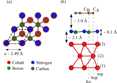
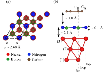
Initial atomic structures were set up with the atomic simulation environment (ASE) (Bahn and Jacobsen, 2002), as follows. The lattice constant of graphene is Å Castro Neto et al. (2009), the one for hBN is Å Catellani et al. (1987), and the one for hcp cobalt is Å Singal and Das (1977). We fix an effective average lattice constant of Å for this well-lattice-matched system, as a compromise to make the lattices commensurable and to keep the unit cell as small as possible. The lattice of graphene is strained by only 1%.
We tested different stacking possibilities and found the energetically preferential structure. In Fig. 1, we show our definition of the unit cell of the graphene/hBN/Co structure. A computational unit cell contains two carbon atoms, and , forming graphene; one boron atom and one nitrogen atom per hBN layer; and three cobalt atoms, one per atomic layer. In general, three positions (top, hcp and fcc) can be distinguished within a hexagonal unit cell. The different positioning possibilities of the carbon atoms above the substrate will influence the strength of the proximity magnetism. We get the lowest-energy configuration when nitrogen atoms are at the top sites and boron atoms are at the fcc sites above Co. Carbon atoms sit on top of boron atoms and at the hollow position above hBN (see Fig. 1). These findings are in agreement with previous DFT studies Bokdam et al. (2013, 2014); Giovannetti et al. (2007). After relaxation of atomic positions we obtained layer distances of Å between the cobalt and hBN and Å between hBN and graphene (measured between C/Co and N atoms, respectively, since the hBN layer is corrugated). The layer distances of this minimum energy configuration are roughly in agreement with those in Refs. Giovannetti et al., 2007; Vanin et al., 2010; Bokdam et al., 2014, which report Å and Å. We also find that the hBN layer is not flat anymore but slightly buckled since the boron atom is closer to the Co surface by Å compared to the nitrogen atom, in agreement with Refs. Bokdam et al., 2014; Grad et al., 2003.
III Effective Hamiltonian
Our main goal is to answer the question, how do hBN and the ferromagnetic substrate affect the graphene Dirac cone at K?
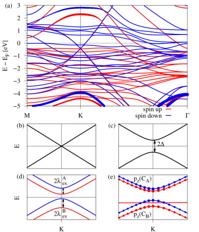
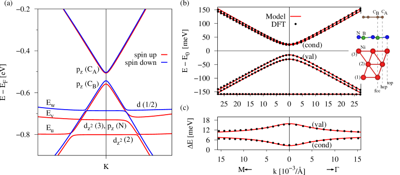
In Fig. 2(a) we show the calculated spin-resolved band structure of the graphene/hBN/Co system (see Fig. 1), along the high-symmetry path M–K– in the energy window from to eV. We can see that the linear dispersion of graphene around the K point is preserved and that the Dirac point is roughly eV below the system Fermi level. Other bands, especially those in the vicinity of the Dirac point energy , originate mainly from the states of the ferromagnet which are located around the Fermi energy. The bands at the K point originating from hBN are far away from the Dirac point, with the highest- (lowest-) lying valence (conduction) band located at eV ( eV) away from the system Fermi level, emphasized by thicker lines in Fig. 2(a). Moreover, hBN becomes spin polarized: its bands spin split by about eV.
III.1 Minimal model
We introduce a minimal Hamiltonian to describe the proximity-induced exchange spin splitting in graphene, similar to earlier derivations of effective Hamiltonians for the proximity spin-orbit coupling in graphene on transition-metal dichalcogenides Gmitra and Fabian (2015); Gmitra et al. (2016) and on the Cu(111) substrate Frank et al. (2016).
Pristine graphene is described by the massless Dirac Hamiltonian in the vicinity of K (K’):
| (1) |
where denotes the Fermi velocity, and are the Cartesian components of the electron wave vector measured from K (K’), and and are the pseudospin Pauli matrices acting on the A and B sublattice orbitals. Hamiltonian describes gapless Dirac states with conical dispersion near Dirac points, with for the K (K’) point, shown in Fig. 2(b).
Since graphene is on a hBN/Co substrate, the carbon atoms from different sublattices feel different potentials, leading to the Hamiltonian
| (2) |
with being the pseudospin Pauli matrix, being the unit spin matrix, and being the proximity-induced orbital gap of the spectrum. The Hamiltonian describes a mass term, which breaks the pseudospin symmetry, and thus describes a gapped graphene dispersion, shown in Fig. 2(c).
To study the proximity exchange, we introduce the Hamiltonian
| (3) | |||||
with and being the exchange parameters for sublattices A and B, respectively. The dispersion of the Hamiltonian is shown in Fig. 2(d), along with the spin character. This term is similar to a sublattice-resolved intrinsic spin-orbit coupling Hamiltonian Gmitra and Fabian (2015); Gmitra et al. (2016); Frank et al. (2016); Gmitra et al. (2013); Irmer et al. (2015); Zollner et al. (2016). The only difference is that it breaks time-reversal symmetry, associated with the magnetization. A close-up in the vicinity of the K point of the DFT band structure is shown in Fig 2(e), supporting the need for a sublattice-resolved exchange Hamiltonian.
The proximity exchange (pex) Hamiltonian,
| (4) |
is a minimal model using only effective carbon orbitals, which can be used to fit the DFT data directly at the K point and extract the pure band splittings. This Hamiltonian can be used for model charge and spin transport calculations. The parameters , , and are related to the band splittings at the K point: splitting of the conduction bands , splitting of the valence bands , and orbital gap , as shown in Figs. 2(c) and 2(d).
The Dirac point is shifted in energy with respect to the system Fermi level by an energy , as can be seen in Fig. 2(a). We call the energy the Dirac point energy, and it will be our measure for the doping level. The Dirac point energy for this model is calculated by averaging the four DFT energies of the graphene Dirac bands at the K point.
III.2 Extended - Hamiltonian
The DFT results in Fig. 2(a) show that in the interesting range of energies of the graphene Dirac bands, there can also lie flat orbitals from Co. When these orbitals hybridize with carbon orbitals in graphene, the effective exchange coupling gets strongly modified. In order to capture this effect quantitatively, we extend our minimal model by a set of orbitals that appear close to the Dirac point. Similar effects occur in graphene on the Cu(111) substrateFrank et al. (2016), for example.
Figure 2(a) shows that in the energy window of meV from the Dirac point, three bands interact with the Dirac states. We then extend our model by adding an effective ferromagnet Hamiltonian , consisting of three bands, which describes the hybridization of the ferromagnet bands with the graphene states. The full effective Hamiltonian in the basis , , , , where u, v, and w label the three orbitals (of the spin specified by the DFT), reads
| (5) |
Here , , are the energies that correspond to the states, and are the effective hybridization parameters with the corresponding Dirac state, where the subscript (superscript) indicates the spin (pseudospin) state. The proximity exchange () and orbital gap () parameters are, in principle, different from those of the minimal Hamiltonian , as they are renormalized due to the hybridization. The hybridization parameters vanish if the Dirac states directly at K are relatively far from the bands. As soon as the Dirac states at K are close to a band or the hybridization is so large that it affects the Dirac states, we can describe the hybridization with the corresponding interaction parameter. We call the Hamiltonian the --model. The energy window of roughly meV from the Dirac point energy can be described by this model rather well (see Figs. 3 and 4).
The - model describes the hybridization between the surface bands of Co with the graphene Dirac states. As we will discuss, this hybridization significantly enhances the effective proximity exchange splitting. Like the minimal model , the - model has to be shifted in energy to match the DFT data. We call this energy , and it is an analog of .
IV Proximity exchange interaction
We present our DFT calculations of the proximity exchange in graphene/hBN/Co and graphene/hBN/Ni for one, two, and three layers of hBN, as well as fits to the effective Hamiltonians. The proximity exchange decreases in magnitude but oscillates as the number of layers changes by one. This oscillating behavior is reminiscent of the oscillatory magnetic interlayer coupling Bruno and Chappert (1992); Bruno (1993).
IV.1 Graphene/hBN/cobalt
IV.1.1 One hBN layer
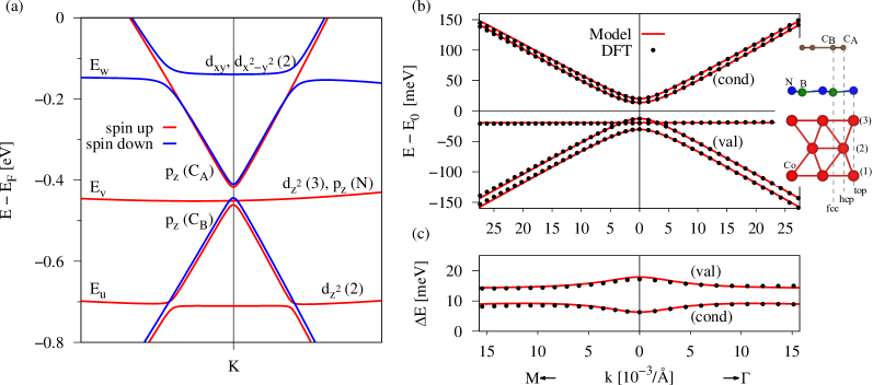
Figure 3(a) shows the spin-polarized band structure of the graphene/hBN/Co heterostructure for one layer of hBN. The graphene Dirac states for spin-up are lying lower in energy than the spin-down ones. The Dirac point energy is below the system Fermi level, corresponding to electron doping of graphene, since the Fermi level now crosses the conduction band of graphene. This shift is induced by the metal, as already suggested in Ref. Giovannetti et al., 2008. The Co bands hybridize with the graphene states in the vicinity of the K point and introduce exchange splitting.
From the band structure in Fig. 3 we see that the linear dispersion of graphene is preserved. In addition, a gap forms, and the spin degeneracy of the Dirac states gets lifted, allowing for semiconducting properties along with the usage of different spin channels by appropriate experimental setups. By comparing our DFT results to the - model Hamiltonian , Eq. (5), we obtain the parameters given in Table 1 for Co as the ferromagnet and one layer of hBN. The fit of the - model is shown in Fig. 3(b) and agrees very well with the DFT data. The gap in the dispersion is found to be roughly meV, while the band splittings are of the order of meV for one layer of hBN.
IV.1.2 Two hBN layers
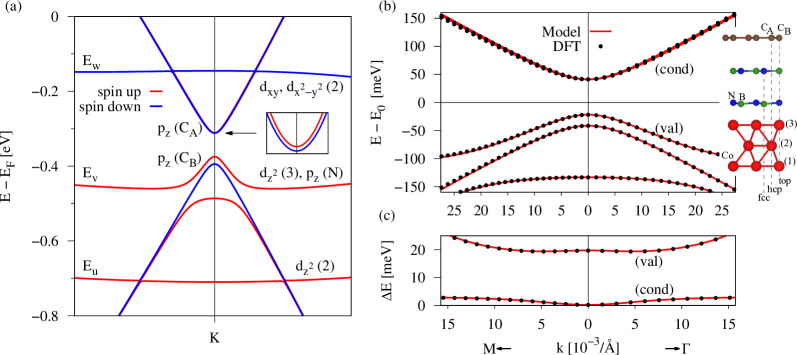
Figure 4 shows the calculated band structure and the fit to the - model in the case of two layers of hBN and three layers of Co. The inset in Fig. 4(b) shows the geometry for two layers of hBN. The relative position of carbon atom to hBN is not changed, while the position of atom is changed, such that it is again on top of the uppermost boron atom, which is the energetically favorable situation for graphene on hBN. The conduction (valence) Dirac states are still formed by sublattice A (B), even though has changed its position within the unit cell. The layer distance between the two hBN layers was relaxed to Å, and the distance between the uppermost hBN layer and graphene is Å in the two-hBN-layer case. The corrugation of the lower hBN and the distance between hBN and Co did not change.
| FM | hBN | IA | ||||||||
|---|---|---|---|---|---|---|---|---|---|---|
| (layers) | (meV) | (meV) | (meV) | (meV) | (meV) | (meV) | (meV) | (meV) | (m/s) | |
| Co | 1 | -430.89 | 21.45 | -7.63 | 8.95 | -279.41 | -19.37 | 282.31 | 48.44 () | 8.12 |
| 2 | -352.65 | 41.02 | 0.096 | -0.512 | -357.12 | -114.75 | 207.34 | 41.67 ( | 8.20 | |
| 3 | -301.07 | 38.83 | -0.005 | 0.018 | -408.70 | -166.03 | 155.10 | 8.21 | ||
| Ni | 1 | -527.98 | 22.98 | -1.25 | 8.17 | -272.58 | -201.27 | -158.17 | 10.15 (, 4.19 () | 8.10 |
| 2 | -435.76 | 42.88 | 0.080 | -1.44 | -363.36 | -309.27 | -251.05 | 32.67 ( | 8.24 | |
| 3 | -361.54 | 40.42 | -0.005 | 0.017 | -437.30 | -384.53 | -324.91 | 8.26 |
Figure 4(a) shows the spin-polarized band structure of graphene/hBN/Co for two layers of hBN. In the band structure, now, the spin-up graphene Dirac states are no longer lying lower in energy than the spin-down ones, leading to a reversal of the sign of the exchange parameters and . The band structure shows that the doping level decreases by roughly meV, and the hybridization with the band with energy , coming from the top Co layer, is strongly enhanced, in contrast to the one-hBN-layer case. The perfect fit to the - model is also seen in Fig. 4(b); the obtained parameters are given in Table 1 for Co as the ferromagnet and two layers of hBN. In Fig. 4(c) we can see that the band splitting at the K point of the conduction (valence) bands is smaller (larger) than in the one-hBN-layer case. In addition, the proximity-induced gap nearly doubles, and the hybridization to the Co state is much stronger.
The inset in Fig. 4(b) shows that for the case of two hBN layers, carbon atom (now at the top site above Co) has a direct connection to the Co atom in the top position via a nitrogen atom and a boron atom of the two individual hBN layers. Localized at this Co atom in the top position, there is some density with character (resulting in the band with energy ) which can propagate through this direct path and polarize carbon atom . This hybridization is described by the parameter , shifting the corresponding bands in energy and leading to the opening of a hybridization gap in the band structure. The vertical stacking of the atoms facilitates the hybridization of the carbon states with Co states. For the case of one hBN layer there is no direct path connecting Co atoms in the top position and carbon atoms , and thus the hybridization is suppressed. Again, by employing our model directly at the K point, we can extract parameters which correspond to the pure splittings of the Dirac bands at the K point, as given in Fig. 4(c).
| FM | hBN (layers) | (meV) | (meV) | (meV) | (meV) |
|---|---|---|---|---|---|
| Co | 1 | -433.10 | 19.25 | -3.14 | 8.59 |
| 2 | -348.03 | 36.44 | 0.097 | -9.81 | |
| 3 | -301.10 | 38.96 | -0.005 | 0.018 | |
| Ni | 1 | -527.89 | 22.86 | -1.40 | 7.78 |
| 2 | -434.82 | 42.04 | 0.068 | -3.38 | |
| 3 | -361.57 | 40.57 | -0.005 | 0.017 |
The values of and , obtained from the two models, are given in Tables 1 and 2. They deviate by a factor of 20, which comes from the fact that the minimal model describes dressed exchange parameters, whereas the - model describes the bare exchange parameters. The dressed parameters contain both the interlayer exchange and spin-selective hybridization of the and orbitals. The bare exchange couplings are much weaker than in the single-hBN-layer case, by an order of magnitude. However, the dressed coupling stays at a similar magnitude (the sign changes). The reason is that the valence-band spin splitting is dominated by the anticrossing of and orbitals, affecting only the spin-up component. The spin-down valence-band is not affected. As a result, the proximity spin splitting is, in this case, caused by shifting the spin-up band relative to its spin-down counterpart, by the spin-selective hybridization. This mechanism of proximity exchange can lead to a giant enhancement of the proximity spin splittings which can be tailored by the electric field.
IV.1.3 Additional considerations
Here we address some outstanding questions related to our above analysis. How do additional insulating layers perform? Can we tune the doping level by an external electric field? Is the proximity exchange affected? Are the band splittings we see representative of a thick ferromagnetic substrate (are three Co layers enough)? How is the proximity effect affected by the Hubbard , which shifts the orbital levels?
In the following we consider only the dressed band splittings , obtained with the minimal model directly at the K point. Bare splittings are barely affected by electric fields, and their behavior with respect to the number of layers is that of a damped oscillator.
Dependence on the number of hBN layers.
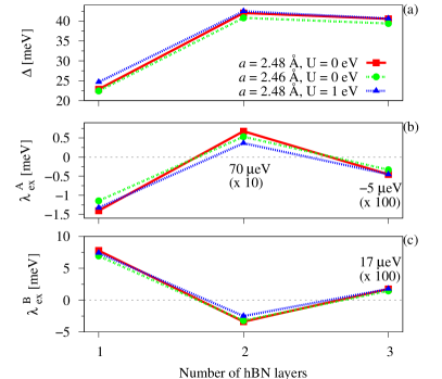
Figure 5 shows the dependence of the proximity gap and the two exchange parameters and on the number of hBN layers between Co and graphene. We can see that the exchange parameters change sign after an additional insulating layer is added. The proximity gap nearly doubles for two layers of hBN and stays essentially unchanged when a third layer is added since the local environment of graphene does not change anymore. The parameters obtained with the minimal proximity exchange model are summarized in Table 2 for Å and Hubbard . For four layers of hBN, again, the parameters change sign, but they are even smaller than for three layers of hBN and thus are not included here. The parameters and are already in the eV regime for three hBN layers, which is a result of the strong barrier. The two-layer case is special for the case of since this exchange parameter has a magnitude similar to that of the single-layer case due to the strong hybridization with the orbitals close to the K point. We note that the distances for the three-layer case are similar to those for the two-layer case. We only have one additional distance between the two hBN layers directly below graphene, which was relaxed to Å.

As we have already seen, the bands of hBN are also spin split. To get the magnitude of the exchange splitting of the individual hBN layers, we look at the graphene/hBN/Co structure with three layers of hBN. In the band structure we can identify the highest- (lowest-) lying valence (conduction) bands, which are spin split, of the three individual layers, like in Fig. 2(a). From that, we extract the band splittings of conduction and valence bands of the individual hBN layers at the K point. The spin-up bands of hBN are always lying lower in energy than the spin-down ones at the K point.
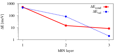
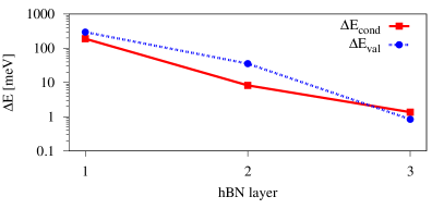
Due to the spin splitting of the bands, hBN can additionally act as a spin filter for tunneling electrons, as reported in Ref. Kamalakar et al., 2016. In Fig. 6 we show the valence- and conduction-band splittings at the K point of the three hBN layers. We find that the exchange splitting of the first hBN layer (closest to the Co surface) is roughly eV. The splittings of the second and third layers are exponentially suppressed, but the third layer still exhibits proximity exchange of more than 1 meV (10 meV for the conduction band).
Lattice-constant effects.
Since we have artificially set the lattice constant for all the (well-lattice-matched) materials to be the same value, we now consider its effect on the proximity structure. We use the graphene constant Å by simply changing the in-plane lattice constant of the slab to this value without changing the vertical distances between the layers, which should be more favorable for the description of the graphene dispersion. The results in this case do not deviate much from the case with our adopted Å, as can be seen in Fig. 5, but the Fermi velocity for Å and one hBN layer is m/s, corresponding to a larger nearest-neighbor hopping parameter of eV.
Hubbard U.
Since the exact position of the bands is crucial to see the giant proximity exchange in the case of two hBN layers, we consider what happens when we apply a Hubbard parameter to the calculation and shift the -orbital levels. From recent studies of graphene on copper Frank et al. (2016) we know that the copper bands have to be shifted down in energy by eV to match the measured band structure from angle-resolved photoemission spectroscopy experiments. From other DFT studies Nakamura et al. (2006); Aryasetiawan et al. (2006); Svane and Gunnarsson (1990); Juhin et al. (2010); Forti et al. (2012), mainly on metal oxides, it is not possible to get a unique value for . Thus we apply eV as a generic representative. The results are shown in Fig. 5. We can see that the parameters and stay almost unchanged, as they are not affected by the strong coupling with orbitals. However, , representing the valence Dirac band splitting is strongly affected, especially in the case of two hBN layers (it is not affected for three layers). By applying the Hubbard , we shift the band with energy in Fig. 4 down, away from the Dirac states, so the splitting at the K point decreases. The energetic position of the bands with respect to the Dirac bands strongly influences the pure band splittings at the K point if the hybridization is large. In the absence of experimental guidance into the exact relative position of levels in our system, we can thus only predict the general trends and rough magnitudes for the valence proximity splitting. If the bands are indeed close to the Dirac point, their influence will be giant, and one can expect ramifications in spin tunneling and spin injection.
Electric field effects.
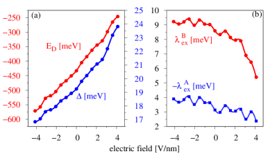
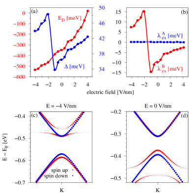
Figure 7 shows the influence of a transverse electric field on the proximity parameters , , and and the Dirac point energy for one layer of hBN. We model our electric field with a saw-like potential oriented perpendicular to the slab structure. A positive field points from cobalt towards graphene and depletes its conduction electrons (lowers the magnitude of ).
We can see that and show the same trend with electric field. In general, by increasing the electric field the doping level decreases; that is, one just shifts the Fermi level with respect to the Dirac bands. The proximity gap also increases with increasing electric field, reflecting the charge transfer away from graphene. The continuous shift of the doping level with the applied electric field allows us to shift the Fermi level to the desired position. The general trend of the proximity parameters is that both tend to decrease with increasing electric field. For moderate field strengths of V/nm, the parameters and thus the band splittings at the K point are almost unaffected.
Most interesting is the two-hBN-layer case since here the valence-band splitting is strongly affected by hybridization with a level. By applying an electric field, we can tune the energetic position of the Dirac point with respect to the levels, which should also strongly affect the spin splitting of the graphene Dirac bands. In Fig. 8 we show the influence of the electric field on the proximity parameters for two layers of hBN. We can see that the Dirac point energy increases with electric field, as for the monolayer hBN case. The proximity parameter stays constant in magnitude around eV. In Figs. 8(c) and 8(d), we show the calculated spin-resolved band structure of the graphene/hBN/Co heterostructure for two hBN layers, projected on the graphene states in the vicinity of the Dirac point for different field strengths. The spin-up graphene valence band at the K point is lying lower in energy than the spin-down one for V/nm and vice versa for V/nm. Therefore the parameter is positive (negative) for fields smaller (larger) than V/nm [see Fig. 8(b)]. The crossover happens at about V/nm. The reason for these reversing spin states is the resonant level. At a certain energetic configuration between the Dirac point and the level, adjusted by the external electric field, the hybridization of the level with graphene valence states leads to the change of the sign of the spin splitting parameters. This allows us to control the sign of the injected spin by applying an electric field, shifting the Dirac bands through the resonant level. (Of course, this effect can only be observed if the bands are indeed close to the Dirac point. DFT calculations can provide, at most, indications of this occurring, due to the insufficient treatment of correlations that are important for orbitals of transition metals.) Also, the proximity gap jumps in magnitude at the same field strength, roughly V/nm, since the parameters and of the model are connected. Apart from the jump, the gap parameter increases with increasing field strength.
Additional cobalt layers.
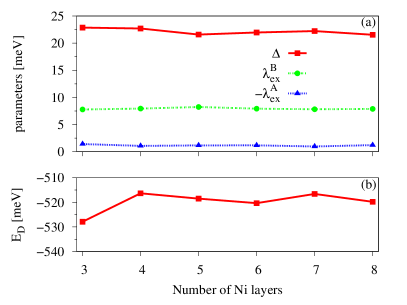
Finally, we analyze the influence of additional Co layers on the band structure (Fig. 9). As we increase the number of Co layers, more bands are introduced into the dispersion. Consequently, in the vicinity of the K point in Fig. 2(a) graphene states can be disturbed by these additional Co bands.
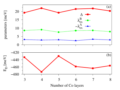
We can see that the band splittings of the graphene Dirac states at the K point do not get influenced much by additional layers, since the parameters and stay almost constant, but the Dirac energy, which is our measure for the doping level, saturates only after six Co layers are present. We conclude that three Co layers suffice to obtain representative proximity parameters, and six Co layers are needed to fix the relative positioning of the bands.
IV.2 Graphene/hBN/nickel
IV.2.1 Structure
We now use Ni as the ferromagnet like in the approach with Co. Nickel crystallizes in a fcc lattice and has a magnetic moment of about , smaller than the one for hcp cobalt, which is Kittel (2004). Thus we expect the effects of proximity-induced magnetism to be smaller for the Ni substrate. In order to stack a hexagonal lattice on top of it, we need to consider the (111) plane. The lattice constant of Ni Kittel (2004) is Å, and thus the lattice constant of the quasi-hexagonal lattice of the (111) plane is Å. As a result, the (111) plane of Ni is suitable for making heterostructures with graphene; the lattice mismatch is small. We fix an effective average lattice constant of Å for the systems with Ni. In this case, the lowest-energy configuration is when nitrogen atoms are at the top sites above Ni and boron atoms are at fcc sites above Ni. Carbon atoms sit on top of boron atoms and at the hollow sites, above the center of a hexagonal ring of hBN (see Fig. 10), in agreement with previous DFT studies Bokdam et al. (2013, 2014); Giovannetti et al. (2007).
After relaxation of atomic positions we obtained layer distances of Å between Ni and hBN and Å between hBN and graphene (measured between C/Ni and N atoms, respectively, since the hBN layer is corrugated).
The layer distances of this minimum-energy configuration are in agreement with Refs. Giovannetti et al., 2007; Vanin et al., 2010; Bokdam et al., 2014, which report Å and Å.
Again, the hBN-layer is not flat anymore but slightly corrugated by Å, in agreement with Refs. Bokdam et al., 2014; Grad et al., 2003.
For hBN we use an AA′ stacking (B over N, N over B), which is the energetically favorable one, with distances between the layers in the range of Å (details are given in sections IV.2.3 and IV.2.4).
IV.2.2 One hBN layer
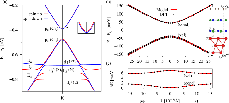
Figure 11(a) shows the calculated spin-polarized band structure of the graphene/hBN/Ni heterostructure for one layer of hBN. The graphene Dirac states for spin up are lying lower in energy than the spin-down ones, as in the Co case. Comparing Ni and Co, we notice that the Dirac point energy for Ni is about meV lower than for Co, but the proximity-induced band splittings are smaller, as expected due to the smaller magnetic moment of Ni. In general the band structures are quite similar, with the difference being that Ni states do not influence the Dirac states as much as Co does. Additionally, we notice that the spin-up bands are formed by the same orbitals as for Co, while the spin-down band near the K point is formed by different orbitals [mixture of orbitals of Ni layers (1/2) except ] due to the different lattices of Ni and Co. Most of all, we notice that there is no band crossing the conduction Dirac states in the relevant energy and region.
The fit to the - model is shown by solid lines to the DFT data in Fig. 11(b). We see that the - model Hamiltonian, Eq. (5), describes our first-principles results very well with the fit parameters given in Table 1. Like in the Co case, the gap in the dispersion is roughly meV, and the band splittings are of the order of meV. We additionally employ our minimal model to extract the effective band spin splittings (see Table 2). Due to the weak hybridization with orbitals, the minimal model parameters are very close to the parameters of the - model.
IV.2.3 Two hBN layers
Figure 12 shows the calculated band structure and the fit to the - model in the case of two layers of hBN and three layers of Ni. Again, the positions of carbon did not change with respect to the hBN layers, while the position of was changed to be on top of the uppermost boron atom. The layer distance between the two hBN layers was relaxed to Å and the distance between the uppermost hBN layer and graphene was Å in the two-layer case. The corrugation of the lower hBN layer and the distance between hBN and Ni did not change. The inset in Fig. 12(b) shows the geometry for two layers of hBN. Figure 12(a) shows the spin-polarized band structure of graphene/hBN/Ni for two layers of hBN. The spin-up graphene Dirac states are again no longer lying lower in energy than the spin-down ones, leading to the reversal of the sign of the exchange parameters, just as for Co. The fit parameters for the - model are given in Table 1. The fit to the - model is shown in Fig. 12(b).
We can see that the band splittings for both the conduction and valence Dirac states are smaller than in the single-hBN-layer case, as expected due to the additional insulating layer, while the proximity-induced gap nearly doubles, and the hybridization to the Ni state is much larger. From the geometry in Fig. 12(b), we can again notice that carbon orbitals can couple to orbitals of Ni in the top position via a nitrogen atom and a boron atom of the two individual hBN layers, which is responsible for the strong hybridization with the band with energy . This hybridization drives the strong proximity exchange in the valence band of graphene.
By employing our minimal model directly at the K point we extract the effective exchange parameters corresponding to the values of the splittings in Fig. 12(c). The parameters are summarized in Table 2. If we compare and , we see that they are of similar magnitudes (unlike for the Co case) since the band with energy is relatively far away from the Dirac point energy, so that the hybridization effects on the band splittings at the K point are similar in monolayer and bilayer hBN structures. There is no resonant level as in the Co case.
IV.2.4 Additional considerations
In the following, we consider effective band splittings directly at the K point, which correspond to the exchange couplings in the minimal model.
Dependence on the number of hBN layers.
Figure 13 shows the dependence of the proximity gap and the two exchange parameters and on the number of hBN layers between Ni and graphene. Again, similar to those for Co, the exchange parameters decrease by one order of magnitude and change sign after an additional insulating layer is added. The proximity gap doubles for two layers of hBN and again stays constant since, effectively, the local environment for graphene does not change anymore the addition of hBN layers. (The distances for the three-layer case are similar to those for the two-layer case.) We have only one additional distance between the two hBN layers directly below graphene, which was relaxed to Å.
Also the bands of hBN are spin split, and like we did for the Co substrate, we look at the graphene/hBN/Ni structure with three layers of hBN. In the band structure we can identify the highest- (lowest-) lying valence (conduction) bands, which are spin split, of the three individual layers. From that, we extract the band splittings of conduction and valence bands of the individual hBN layers at the K point. We notice that the spin-up bands of hBN are always lying lower in energy than the spin-down ones. In Fig. 14 we show the valence- and conduction-band splittings at the K point of the three layers. The splittings are very similar to, but smaller in magnitude than, those in the Co case. The spin splitting of the bands from the first layer is roughly meV.
Lattice-constant effects.
We also look at how the band structure of the slabs changes when we use the graphene lattice constant for all the materials, Å, by simply changing the in-plane lattice constant to this value without changing the vertical distances between the layers. The results in this case do not deviate much from the case with Å, as can be seen in Fig. 13. The Fermi velocity for Å and one hBN layer is m/s, corresponding to a larger nearest-neighbor hopping parameter of eV.
Hubbard U.
We now introduce a Hubbard parameter eV to compare the results of the calculations of different numbers of layers of hBN with the ones with eV. This comparison is in Fig. 13. In contrast to the case of Co, the proximity effects are barely affected by the positioning of the levels since the levels are quite far from the Dirac point. We can conclude that the predicted large proximity exchange splitting in the Dirac valence band is robust.
Electric field effects.
Figure 15 shows the influence of the electric field on the proximity parameters and the doping level. We can see that and show the same trend with electric field. By increasing the electric field the doping level decreases. The proximity gap also increases with increasing electric field, reflecting the charge transfer away from graphene. The continuous shift of the doping level with the applied electric field allows us to shift the Fermi level to the desired position. Compared to those in the case of Co, the proximity parameters for Ni change more smoothly with applied electric field. The magnitude of the proximity parameter , on average, stays constant with electric field. The magnitude of the parameter slowly decreases with electric field, but for moderate fields the band splittings are almost unchanged. The electric tunability of the proximity exchange in this case is rather weak.
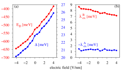
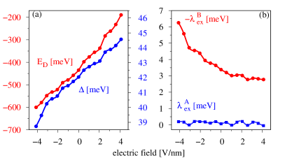
Figure 16 shows the influence of the electric field on the proximity parameters and the doping level for two hBN layers. We can see that and show the same trend with electric field as for the single-layer hBN, but the orbital gap parameter is roughly two times larger than in the case with monolayer hBN. As we have already seen, the two proximity parameters change their sign with the addition of the second hBN layer. The magnitude of the proximity parameter stays roughly constant with electric field but is one order of magnitude smaller than in the monolayer hBN case.
The proximity parameter decreases with increasing electric field. For negative (positive) fields, the Dirac point is shifted in energy towards (away from) the hybridizing levels, which cross the valence Dirac states (see Fig. 12), and is increasing (decreasing). We note that the magnitude of in the bilayer hBN case is comparable to that in the monolayer hBN case.
Additional nickel layers.
Finally, we analyze the influence of additional Ni layers on the band structure (see Fig. 17). As we increase the number of Ni layers, more bands are also introduced into the dispersion. Consequently, in the vicinity of the K point graphene Dirac states can be disturbed by these additional Ni bands. We can see that the band splittings of graphene at the K point do not get influenced much by additional layers since the parameters stay at the same order. In this case, already, four layers of Ni show a steady situation for the Dirac energy . The effect on the proximity parameters is negligible.
V Summary and Conclusions
We investigated the proximity-induced exchange interaction induced by the ferromagnets Co and Ni into graphene through the insulator hBN. We found proximity-induced exchange splittings of up to meV together with a proximity gap of meV for one layer of hBN. As more insulating layers are introduced, the proximity-induced exchange interaction in general decreases exponentially, but the signs of the exchange parameters reverse. This reversal of the signs continues for up to four layers of hBN. We also introduced a minimal model and an extended model to fit the first-principles data. The model parameters are summarized in Tables 1 and 2.
A fascinating case is that of Co. Here a rather flat level strongly hybridizes with graphene orbitals in the valence band, leading to a giant proximity exchange in the case of two hBN layers. Since this giant exchange depends on the offset of the orbital energy and the Dirac point, we found that an external transverse electric field can tune this effect, and even lead to a crossover between positive and negative induced spin polarization in the valence band of graphene. We found that in general the results for both ferromagnets are similar, although the effects of Co are stronger than those of Ni, which is a consequence of the smaller atomic magnetic moment of the latter. The main difference between Co and Ni lies in the orbital decomposition of the bands, which interact with the graphene Dirac states, and leads to the giant spin splitting of the valence band in the case of Co.
VI Acknowledgments
This work was supported by DFG SFB Grant No. 689 and GRK Grant No. 1570 and by the EU Seventh Framework Programme under Grant Agreement No. 604391 Graphene Flagship.
References
- Han et al. (2014) W. Han, R. K. Kawakami, M. Gmitra, and J. Fabian, Nat Nano 9, 794 (2014).
- Yazyev (2010) O. V. Yazyev, Rep. Prog. Phys. 73, 056501 (2010).
- Yazyev and Helm (2007) O. V. Yazyev and L. Helm, Phys. Rev. B 75, 125408 (2007).
- Wehling et al. (2007) T. O. Wehling, A. V. Balatsky, M. I. Katsnelson, A. I. Lichtenstein, K. Scharnberg, and R. Wiesendanger, Phys. Rev. B 75, 125425 (2007).
- McCreary et al. (2012) K. M. McCreary, A. G. Swartz, W. Han, J. Fabian, and R. K. Kawakami, Phys. Rev. Lett. 109, 186604 (2012).
- González-Herrero et al. (2016) H. González-Herrero, J. M. Gómez-Rodríguez, P. Mallet, M. Moaied, J. J. Palacios, C. Salgado, M. M. Ugeda, J.-y. Veuillen, F. Yndurain, and I. Brihuega, Science 352, 437 (2016).
- Ding et al. (2011) J. Ding, Z. Qiao, W. Feng, Y. Yao, and Q. Niu, Phys. Rev. B 84, 195444 (2011).
- Castro Neto and Guinea (2009) A. H. Castro Neto and F. Guinea, Phys. Rev. Lett. 103, 026804 (2009).
- Gmitra et al. (2013) M. Gmitra, D. Kochan, and J. Fabian, Phys. Rev. Lett. 110, 246602 (2013).
- Zhou et al. (2010) J. Zhou, Q. Liang, and J. Dong, Carbon 48, 1405 (2010).
- Irmer et al. (2015) S. Irmer, T. Frank, S. Putz, M. Gmitra, D. Kochan, and J. Fabian, Phys. Rev. B 91, 115141 (2015).
- Guzmán-Arellano et al. (2015) R. M. Guzmán-Arellano, A. D. Hernández-Nieves, C. A. Balseiro, and G. Usaj, Phys. Rev. B 91, 195408 (2015).
- Fedorov et al. (2013) D. V. Fedorov, M. Gradhand, S. Ostanin, I. V. Maznichenko, A. Ernst, J. Fabian, and I. Mertig, Phys. Rev. Lett. 110, 156602 (2013).
- Weeks et al. (2011) C. Weeks, J. Hu, J. Alicea, M. Franz, and R. Wu, Phys. Rev. X 1, 021001 (2011).
- Balakrishnan et al. (2013) J. Balakrishnan, G. Kok Wai Koon, M. Jaiswal, a. H. Castro Neto, and B. Özyilmaz, Nat. Phys. 9, 284 (2013).
- Zollner et al. (2016) K. Zollner, T. Frank, S. Irmer, M. Gmitra, D. Kochan, and J. Fabian, Phys. Rev. B 93, 045423 (2016).
- Kochan et al. (2014) D. Kochan, M. Gmitra, and J. Fabian, Phys. Rev. Lett. 112, 116602 (2014).
- Ferreira et al. (2014) A. Ferreira, T. G. Rappoport, M. A. Cazalilla, and A. H. Castro Neto, Phys. Rev. Lett. 112, 066601 (2014).
- Wilhelm et al. (2015) J. Wilhelm, M. Walz, and F. Evers, Phys. Rev. B 92, 014405 (2015).
- Thomsen et al. (2015) M. R. Thomsen, M. M. Ervasti, A. Harju, and T. G. Pedersen, Phys. Rev. B 92, 195408 (2015).
- Van Tuan and Roche (2016) D. Van Tuan and S. Roche, Phys. Rev. Lett. 116, 106601 (2016).
- Bundesmann et al. (2015) J. Bundesmann, D. Kochan, F. Tkatschenko, J. Fabian, and K. Richter, Phys. Rev. B 92, 081403 (2015).
- Yang et al. (2013) H. X. Yang, A. Hallal, D. Terrade, X. Waintal, S. Roche, and M. Chshiev, Phys. Rev. Lett. 110, 046603 (2013).
- Qiao et al. (2014) Z. Qiao, W. Ren, H. Chen, L. Bellaiche, Z. Zhang, A. H. MacDonald, and Q. Niu, Phys. Rev. Lett. 112, 116404 (2014).
- Zutic et al. (2004) I. Zutic, J. Fabian, and S. Das Sarma, Rev. Mod. Phys. 76, 323 (2004).
- Fabian et al. (2007) J. Fabian, A. Matos-Abiague, C. Ertler, P. Stano, and I. Zutic, Acta Phys. Slovaca 57, 565 (2007).
- Wang et al. (2015) Z. Wang, C. Tang, R. Sachs, Y. Barlas, and J. Shi, Phys. Rev. Lett. 114, 016603 (2015).
- Leutenantsmeyer et al. (2016) J. C. Leutenantsmeyer, A. A. Kaverzin, M. Wojtaszek, and B. J. van Wees, arXiv:1601.00995 (2016).
- Wei et al. (2016) P. Wei, S. Lee, F. Lemaitre, L. Pinel, D. Cutaia, W. Cha, F. Katmis, Y. Zhu, D. Heiman, J. Hone, J. S. Moodera, and C.-T. Chen, Nat. Mater. 15, 711 (2016).
- Tombros et al. (2007) N. Tombros, C. Jozsa, M. Popinciuc, H. T. Jonkman, and B. J. van Wees, Nature 448, 571 (2007).
- Ohishi et al. (2007) M. Ohishi, M. Shiraishi, R. Nouchi, T. Nozaki, T. Shinjo, and Y. Suzuki, Jpn. J. Appl. Phys. 46, L605 (2007).
- Yamaguchi et al. (2013) T. Yamaguchi, Y. Inoue, S. Masubuchi, S. Morikawa, M. Onuki, K. Watanabe, T. Taniguchi, R. Moriya, and T. Machida, Appl. Phys. Express 6, 073001 (2013).
- Yamaguchi et al. (2012) T. Yamaguchi, S. Masubuchi, K. Iguchi, R. Moriya, and T. Machida, J. Magn. Magn. Mater. 324, 849 (2012).
- Volmer et al. (2013) F. Volmer, M. Drögeler, E. Maynicke, N. von den Driesch, M. L. Boschen, G. Güntherodt, and B. Beschoten, Phys. Rev. B 88, 161405 (2013).
- Volmer et al. (2015) F. Volmer, M. Drögeler, G. Güntherodt, C. Stampfer, and B. Beschoten, Synthetic Metals 210, Part A, 42 (2015).
- Han et al. (2010) W. Han, K. Pi, K. M. McCreary, Y. Li, J. J. I. Wong, A. G. Swartz, and R. K. Kawakami, Phys. Rev. Lett. 105, 167202 (2010).
- Patra et al. (2012) A. K. Patra, S. Singh, B. Barin, Y. Lee, J.-H. Ahn, E. del Barco, E. R. Mucciolo, and B. Özyilmaz, Appl. Phys. Lett. 101, 162407 (2012).
- Kamalakar et al. (2014) M. V. Kamalakar, A. Dankert, J. Bergsten, T. Ive, and S. P. Dash, Sci. Rep. 4, 6146 (2014).
- Kamalakar et al. (2016) M. V. Kamalakar, A. Dankert, P. J. Kelly, and S. P. Dash, Scientific Reports 6, 21168 (2016).
- Wu et al. (2014) Q. Wu, L. Shen, Z. Bai, M. Zeng, M. Yang, Z. Huang, and Y. P. Feng, Phys. Rev. Applied 2, 044008 (2014).
- Martin et al. (2015) M.-B. Martin, B. Dlubak, R. S. Weatherup, M. Piquemal-Banci, H. Yang, R. Blume, R. Schloegl, S. Collin, F. Petroff, S. Hofmann, J. Robertson, A. Anane, A. Fert, and P. Seneor, Appl. Phys. Lett. 107, 012408 (2015).
- Dlubak et al. (2012) B. Dlubak, M. B. Martin, R. S. Weatherup, H. Yang, C. Deranlot, R. Blume, R. Schloegl, A. Fert, A. Anane, S. Hofmann, P. Seneor, and J. Robertson, ACS Nano 6, 10930 (2012).
- Karpan et al. (2007) V. M. Karpan, G. Giovannetti, P. A. Khomyakov, M. Talanana, A. A. Starikov, M. Zwierzycki, J. van den Brink, G. Brocks, and P. J. Kelly, Phys. Rev. Lett. 99, 176602 (2007).
- Lazić et al. (2014) P. Lazić, G. M. Sipahi, R. K. Kawakami, and I. Žutić, Phys. Rev. B 90, 085429 (2014).
- Yang et al. (2016) H. Yang, A. D. Vu, A. Hallal, N. Rougemaille, J. Coraux, G. Chen, A. K. Schmid, and M. Chshiev, Nano Lett. 16, 145 (2016).
- Giovannetti et al. (2007) G. Giovannetti, P. A. Khomyakov, G. Brocks, P. J. Kelly, and J. van den Brink, Phys. Rev. B 76, 073103 (2007).
- Britnell et al. (2012) L. Britnell, R. V. Gorbachev, R. Jalil, B. D. Belle, F. Schedin, a. Mishchenko, T. Georgiou, M. I. Katsnelson, L. Eaves, S. V. Morozov, N. M. R. Peres, J. Leist, a. K. Geim, K. S. Novoselov, and L. a. Ponomarenko, Science 335, 947 (2012).
- Giovannetti et al. (2008) G. Giovannetti, P. A. Khomyakov, G. Brocks, V. M. Karpan, J. van den Brink, and P. J. Kelly, Physical Review Letters 101, 026803 (2008).
- Frank et al. (2016) T. Frank, M. Gmitra, and J. Fabian, Phys. Rev. B 93, 155142 (2016).
- Lazić et al. (2016) P. Lazić, K. D. Belashchenko, and I. Žutić, Phys. Rev. B 93, 241401 (2016).
- Bruno (1993) P. Bruno, EPL 23, 615 (1993).
- Hohenberg and Kohn (1964) P. Hohenberg and W. Kohn, Phys. Rev. 136, B864 (1964).
- Giannozzi et al. (2009) P. Giannozzi, S. Baroni, N. Bonini, M. Calandra, R. Car, C. Cavazzoni, D. Ceresoli, G. L. Chiarotti, M. Cococcioni, I. Dabo, A. Dal Corso, S. de Gironcoli, S. Fabris, G. Fratesi, R. Gebauer, U. Gerstmann, C. Gougoussis, A. Kokalj, M. Lazzeri, L. Martin-Samos, N. Marzari, F. Mauri, R. Mazzarello, S. Paolini, A. Pasquarello, L. Paulatto, C. Sbraccia, S. Scandolo, G. Sclauzero, A. P. Seitsonen, A. Smogunov, P. Umari, and R. M. Wentzcovitch, J. Phys. Condens. Matter 21, 395502 (2009).
- Note (1) An analysis on the importance of an accurate -point sampling is included in Ref. \rev@citealpnumBokdam2013.
- Kresse and Joubert (1999) G. Kresse and D. Joubert, Phys. Rev. B 59, 1758 (1999).
- Perdew et al. (1996) J. P. Perdew, K. Burke, and M. Ernzerhof, Phys. Rev. Lett. 77, 3865 (1996).
- Grimme (2006) S. Grimme, Journal of Computational Chemistry 27, 1787 (2006).
- J. E. Dennis and Moré (1977) J. J. E. Dennis and J. J. Moré, SIAM Rev. 19, 46 (1977).
- Bengtsson (1999) L. Bengtsson, Physical Review B 59, 12301 (1999).
- Bahn and Jacobsen (2002) S. R. Bahn and K. W. Jacobsen, Comput. Sci. Eng. 4, 56 (2002).
- Castro Neto et al. (2009) A. H. Castro Neto, F. Guinea, N. M. R. Peres, K. S. Novoselov, and a. K. Geim, Rev. Mod. Phys. 81, 109 (2009).
- Catellani et al. (1987) A. Catellani, M. Posternak, A. Baldereschi, and A. J. Freeman, Phys. Rev. B 36, 6105 (1987).
- Singal and Das (1977) C. M. Singal and T. P. Das, Phys. Rev. B 16, 5068 (1977).
- Bokdam et al. (2013) M. Bokdam, P. A. Khomyakov, G. Brocks, and P. J. Kelly, Phys. Rev. B 87, 075414 (2013).
- Bokdam et al. (2014) M. Bokdam, G. Brocks, M. I. Katsnelson, and P. J. Kelly, Physical Review B 90, 085415 (2014).
- Vanin et al. (2010) M. Vanin, J. J. Mortensen, A. K. Kelkkanen, J. M. Garcia-Lastra, K. S. Thygesen, and K. W. Jacobsen, Phys. Rev. B 81, 081408 (2010).
- Grad et al. (2003) G. B. Grad, P. Blaha, K. Schwarz, W. Auwärter, and T. Greber, Phys. Rev. B 68, 085404 (2003).
- Pease (1952) R. S. Pease, Acta Crystallographica 5, 356 (1952).
- Gmitra and Fabian (2015) M. Gmitra and J. Fabian, Phys. Rev. B 92, 155403 (2015).
- Gmitra et al. (2016) M. Gmitra, D. Kochan, P. Högl, and J. Fabian, Phys. Rev. B 93, 155104 (2016).
- Bruno and Chappert (1992) P. Bruno and C. Chappert, Physical Review B 46, 261 (1992).
- Nakamura et al. (2006) K. Nakamura, R. Arita, Y. Yoshimoto, and S. Tsuneyuki, Phys. Rev. B 74, 235113 (2006).
- Aryasetiawan et al. (2006) F. Aryasetiawan, K. Karlsson, O. Jepsen, and U. Schönberger, Phys. Rev. B 74, 125106 (2006).
- Svane and Gunnarsson (1990) A. Svane and O. Gunnarsson, Phys. Rev. Lett. 65, 1148 (1990).
- Juhin et al. (2010) A. Juhin, F. de Groot, G. Vankó, M. Calandra, and C. Brouder, Phys. Rev. B 81, 115115 (2010).
- Forti et al. (2012) M. Forti, P. Alonso, P. Gargano, and G. Rubiolo, Procedia Materials Science 1, 230 (2012).
- Kittel (2004) C. Kittel, Introduction to Solid State Physics (Wiley, 2004).