The role of exchange interaction in nitrogen vacancy centre-based magnetometry
Abstract
We propose a multilayer device comprising of a thin-film-based ferromagnetic hetero-structure (FMH) deposited on a diamond layer doped with nitrogen vacancy centers (NVC’s). We find that when the NVC’s are in close proximity (1-2 nm) with the FMH, the exchange energy is comparable to, and may even surpass the magnetostatic interaction energy. This calls for the need to consider and utilize both effects in magnetometry based on NVC’s in diamond. As the distance between the FMH and NVC is decreased to the sub-nanometer scale, the exponential increase in the exchange energy suggests spintronic applications of NVC beyond magnetometry, such as detection of spin-Hall effect or spin currents.
pacs:
75.30.Et, 76.30.Mi, 75.50.-yI Introduction
Ferromagnetic hetero-structures (FMH) are integral spintronic elements that play a critical role in various spin transport phenomena. FMH have been used as a platform for practical spintronic devices, such as spin-Hall Jungwirth et al. (2012); Wunderlich et al. (2009, 2010); Seki et al. (2008); Mihajlović et al. (2009) and spin-orbit-based memories Jalil and Tan (2014); Kent and Worledge (2015); Matsukura et al. (2015), anomalous Hall, and topological Hall-based sensors Ni et al. (2016). In such systems, the spin density can be detected by many methods, such as magneto-optic Kerr effect (MOKE) Kato et al. (2004); Vernier et al. (2014), ferromagnetic resonance (FMR) Liu et al. (2016), and electrical measurements Lou et al. (2006, 2007). In the characterization of the FMH devices, a spatial resolution of the spin distribution up to the order of has been achieved by MOKE Vernier et al. (2014), and up to sub- using magnetic force microscopy (MFM) Martin and Wickramasinghe (1987). However, with the advancement of device fabrication at nanoscale, it requires detection and imaging technique that can provide nanoscale resolution as well as high sensitivity.
Recently, the nitrogen-vacancy centers (NVC’s) in diamond have been employed as extremely sensitive vector magnetic field sensors operating at room temperature and capable of nanoscale spatial resolution Taylor et al. (2008a); Van der Sar et al. (2015); Arai et al. (2015); Rugar et al. (2015); DeVience et al. (2015); Grinolds et al. (2014); Degen (2008); Manson et al. (2006); Acosta and Hemmer (2013); Hingant et al. (2015). NVC’s are atomic-scale defects which are formed either naturally or by implantation, using high-energy nitrogen ion beam Ofori-Okai et al. (2012), annealing Naydenov et al. (2010); Schwartz et al. (2014), and nitrogen doping Ohno et al. (2012). The NVC spin states are split under the influence of an external magnetic field. Such spin-splitting selectively suppresses optical fluorescence, making it possible to achieve measurements of the magnetic field through optically detected magnetic resonance (ODMR) Rondin et al. (2014); Balasubramanian et al. (2008); Taylor et al. (2008b); Jelezko et al. (2004); Childress et al. (2006); De Lange et al. (2010); Ryan et al. (2010).
In conventional magnetometry experiments Rondin et al. (2014), the distance between the NVC and the detected magnetic moment of an electron is large enough so that only the Zeeman effect has to be considered. The Zeeman effect arises from dipole-dipole interaction which is long range by nature. In sensing the magnetic field profile, a higher spatial resolution can be achieved if the sensor is brought closer to the detected system Taylor et al. (2008a); Degen (2008); Rondin et al. (2014). At the same time, it has been recently shown that the diamond could be reduced to nanometer scale Tisler et al. (2011); Mochalin et al. (2012); Gong et al. (2016) and an NVC could be positioned at a distance of nm below the diamond surface Loretz et al. (2014); Acosta et al. (2009); Ofori-Okai et al. (2012), thus minimizing the separation between the NVC sensor and the target spin. However, when the sensor is positioned very close to the sample, the electron in NVC can interact with the electron in the sample through the exchange mechanism, in addition to the usual dipole-dipole interaction. In contrast to the dipole interaction, the exchange effect is short range because it depends on the overlap of the NVC wavefunction with that of the magnetic moment . Therefore, it is important to explore the full nature of electron-electron interaction, i.e., both the dipole coupling and the exchange coupling, when the NVC is placed in close proximity to the FHM. Recently, the exchange interaction between the ferromagnetic tip and the magnetic sample has also been considered in magnetic exchange force microscopy (MExFM) Kaiser et al. (2007); Pielmeier and Giessibl (2013); Granovskij et al. (2014). However, to the best of our knowledge, the exchange interaction between proximal NVC spins and FMH spins, has not been considered in NV-based magnetometry. This study will thus be highly relevant for advancing NV-based magnetometry towards its ultimate spatial resolution.
The outline of this paper is as follows. In Sec. II we formulate the theory of the exchange coupling between FMH spin and NVC spin. In Sec. III we provide numerical calculation of the exchange coupling, and discuss the feasibility of the proposed scheme and analyze its application in magnetometry. Section IV is the conclusion.
II THEORY
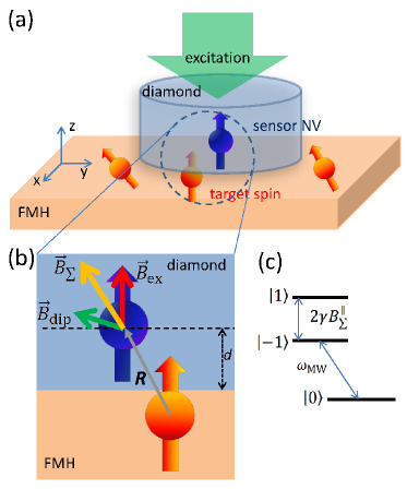
The conceptual device is illustrated in Fig. 1. We consider a diamond layer engineered such that NVC’s are located in close proximity to the diamond surface. Subsequently, a FMH layer is deposited on top of the diamond surface such that the average distance between the of the FMH and the NVC is of the order of a few nanometers Loretz et al. (2014); Acosta et al. (2009); Ofori-Okai et al. (2012).
The magnetic dipole field due to the magnetic moment is given by , is the displacement from the magnetic moment, and are the Cartesian coordinates of the 2D-plane containing the FMH/diamond interface. The Zeeman magnetic energy (dipole coupling) is given by , where is the magnetic moment of the NVC. On the other hand, the exchange energy is given by , where is the exchange field, with the exchange coupling coefficient dependent on the distance between the NVC and the magnetic moment. Phenomenologically, the distance dependence can be expressed as , with being the decay constant. In the following we will analyze in detail the effect of the exchange interaction on the readout of the NVC response and compare it to the effect of the dipole interaction .
II.1 Theory of exchange energy
The wavefunction for a NVC-FMH system with parallel and anti-parallel spin alignments is given, respectively by:
| (1) | |||||
| (2) | |||||
where is the NVC electron wavefunction centered at the vacancy (the origin), and is the FMH electron wavefunction located at , and represents spin state of electron at the NVC (FMH), respectively, with being spin quantum numbers. The parallel wavefunction derives its anti-symmetric property from exchange of position, while the anti-parallel wavefunction derives its antisymmetry from spin exchange. The two-particle wavefunction captures the exchange interaction between NVC and FMH. The interaction strength is determined from the coupling constants:
| (3) | |||
| (4) |
in which is the interaction energy between two particles carrying charge and spin, where is the Coulomb energy, and is the magnetic dipole interaction energy, with . Parallel and anti-parallel configurations (with respect to the spin quantization axis of the NVC) have the same direct coupling energy , while their exchange energy is opposite in sign. Thus, the exchange physics enables the sensing of orientation of the moment in the FMH:
| (5) |
The above exchange interaction energies modify the unperturbed Hamiltonian of the NVC-FMH system, which can be found, e.g., in Doherty et al. (2012). Explicitly, we have
| (6) |
The index represents the FMH spin center at location , which will be summed over the total number of spin centers in the FMH layer. Physically, the above exchange energy may be expressed as , where the exchange constant is a positive scalar with an energy unit (e.g., eV), while is either for P/AP alignment.
II.2 Wavefunction of electron spin in FMH
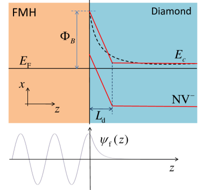
We assume that a Schottky type barrier is formed at the FMH/diamond interface, with the potential being a function of the distance between the NVC and the interface. The wavefunction of the FMH penetrates into the diamond, where it exhibits an exponential decay , where is a decay function and is the distance from the FMH/diamond interface. Based on the WKB approximation, the decay function can be expressed as , with being the electron energy. Taking into account the overlap of the FMH wavefunction within the barrier, the wavefunction of one spin center in the FMH/diamond system can be expressed as follows:
| (7) |
In the above, is the in-plane wavefunction, and in the case of free electron, , and , are the normalization constants. is the distribution function of the FMH wavefunction in the FMH plane, which can have, for example, a Gaussian form , with is the position of FMH spin, and is the width of its wavefunction. For simplicity, the Schottky barrier potential can be approximated as a linear function , where is the Schottky barrier height at the FMH/diamond interface, is the bottom of the conduction band of the diamond, and is the depletion length. In this way, the analytical expression of the decaying function and wavefunction can be evaluated, see Appendix A for details.
II.3 Wavefunction of electron spin in NVC
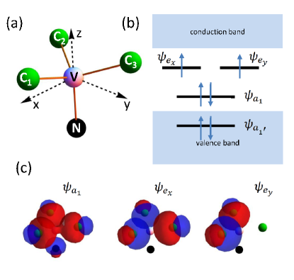
The NVC, in turn, comprises of wavefunctions , and which can be derived from standard hybridization and normalization approaches. The nitrogen atom takes on the configurations along the -direction, while carbon atom takes on the configurations along the -plane, see in Fig. 2. With the vacancy placed at the origin of coordinates, the relative locations of the atoms are fixed. The four wavefunctions are to be re-parameterized as to account for a common origin V, see Appendix B. In the NVC, the individual atomic wavefunctions mix to produce , which are expressed as Hossain et al. (2008)
| (8) | |||||
with and being the orbital overlap integrals. For these simple wavefunctions and . Furthermore, the coupling between and results in hybridized eigenstates and . Although there are six electrons in the NVC, two of the electrons occupy state which lie deep within the valence band Doherty et al. (2012), and hence have negligible contribution to the optical property of the NVC Doherty et al. (2012). Hence, we need to consider only four electrons, which occupy the states . In bulk diamond, the expanse of the NVC wavefunction is less than 1 nm Gali et al. (2008); Hossain et al. (2008).
III Results and Discussions
III.1 Numerical estimation
Using the NVC wavefunction given by Eq. 8, we can make an estimate of the zero-field ground state splitting, which is essentially a direct exchange between and states, involving the magnetic field energy. The zero-field ground state splitting is given by Doherty et al. (2012)
| (9) |
where . The estimated ground state splitting is found to be GHz which is close to the measured value of 2.87 GHz Acosta and Hemmer (2013). Having affirmed reasonable accuracy of the chosen NVC wavefunction, we consider the NVC-FMH system shown in Fig. 1 and Fig. 2, with parallel spin alignment represented by and anti-parallel spin alignment represented by . For simplicity, we consider just the state for an NVC deliberately designed to be a spin up pointing vertically to the FMH plane. The NVC wavefunction overlaps with emanating from one particular spin center at the FMH. As there are many FMH spin centers, the total effect is summed over the volume of the FMH.
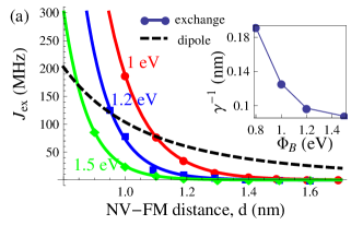
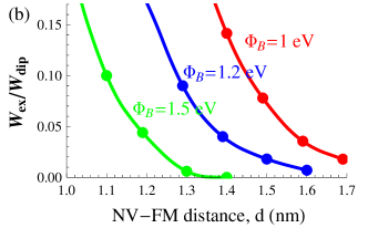
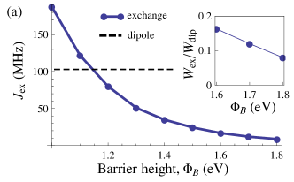
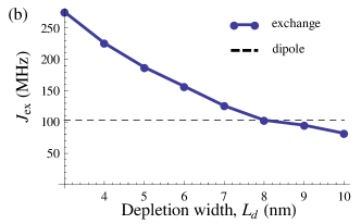
Results of our calculated exchange coupling between NVC spin and one FMH spin are shown in Fig. 3. First, it shows that the exchange coupling exponentially decays with respect to the FMH-NVC distance. The phenomenological formula of the exchange coupling gives a good fit to our numerical results, confirming the sensitivity of the exchange coupling to the distance. Second, a low barrier height and narrow depletion region, which allows deep wavefunction penetration into the diamond, are very important pre-conditions to achieve significant exchange energy, see Fig. 4.
Meanwhile, as it was shown earlier, the interface Schottky barrier is almost constant regardless of the doping level Sun and Ang (2012), it can be controlled by applying a bias voltage. However, this is limited by the electro-chemical property of the interface as high voltage may lead to the surface oxidation Grotz et al. (2012). An alternative way to reduce the barrier height at the interface is to terminate the diamond surface with elements that induce a large positive electron affinity (PEA), since the Schottky barrier at the interface is roughly determined by the difference between the work function of the metal and the electron affinity of diamond, i.e., . For example, diamond with an oxygen-terminated surface has a PEA value of eV Maier et al. (2001), while that with a chlorine-terminated surface has eV Tiwari et al. (2011), and that with a fluorine-terminated surface has eV Rietwyk et al. (2013). With the above PEA values and typical work function value of metals eV, the barrier can be reduced to eV. A combination of applied bias and choice of surface termination can result in a significant reduction of the barrier height down to eV, which would allow significant penetration of the FMH electron wavefunction into diamond.
At the same time, the depletion region can be reduced by increasing the doping concentration or by applying a gate voltage across the FMH/diamond interface Grotz et al. (2012); Geis et al. (1996a, b); Sun and Ang (2012). In diamond doped with nitrogen (), the depletion width is determined by , where is the intrinsic build-in potential Santori et al. (2009); Sun and Ang (2012), is applied voltage, is the dielectric constant of a diamond, and is the vacuum permittivity. For example, a depletion width of 10 nm can be achieved with an implantation dose of 10 ppm (), and it can be reduced to 3 nm for a dose of 100 ppm (). As discussed later, this narrow depletion width is also crucial for stability of negatively-charged NV centers, but high implantation dose will degrade the spin-coherence of the NV centers. In general, a wider depletion width will reduce the wavefunction overlap between the NV center and the magnetic moment in the FM layer, and hence the exchange coupling between the two. However, the degree of the overlap (and thus the strength of the exchange coupling) is a weaker function of the depletion width compared to that of the Schottky barrier height (see Appendix A). For instance even at a depletion width of 10 nm, the exchange coupling strength is still roughly of the same order of magnitude as that corresponding to a depletion width of a few nm (say 3 nm) - see Fig. 4(b).
Given the FMH/NVC distance achievable by today’s technology of about 1-2 nm, a barrier height (with respect to the Fermi level of FMH) of less than 1 eV will already result in the exchange energy surpassing the magnetic energy (see Fig. 3 (a)). Under this circumstance, it is essential to consider the NVC-FMH exchange interaction in the design of NVC-based magnetometry devices. Both magnetic and exchange energies are estimated to be at the order of a few hundred MHz of the 2.87 GHz zero field splitting of the NVC. For separation distance more than 2 nm, the exchange energy rapidly decreases to zero, at a much faster rate than the dipole coupling energy ( see Fig.3). This is consistent with prevailing experimental focus on using only the magnetic energy in describing the results of the magnetometry experiments. Considering ongoing progress in development of etching and lithography tools which become increasingly capable of producing hetero-structures with small distances between NVC and the interface, it makes perfect sense to start considering the short-range exchange effect.
III.2 Stability of shallow centers
Now we will discuss about the stability of the negatively-charged centers near the FMH/diamond interface, which would be a crucial factor for the feasibility of our scheme. The charged state of an NV center depends on the transition level relative to the Fermi level. In diamond doped with nitrogen, the Fermi level is 1.7 eV below the conduction band minimum (CBM) Collins (2002); Farrer (1969) , and the level is 2.58 eV below the CBM Weber et al. (2010); Steeds et al. (2000). Thus, in free-standing nitrogen-doped diamond, the NV centers deep in the bulk diamond are likely to be in the state ( in Fig. 5 (a)). When the diamond with hydrogen-terminated surface is in contact with metal Geis et al. (1996a, b); Sun and Ang (2012) or air Hauf et al. (2011) , part of the level would be raised above the Fermi level due to the band bending near the interface Hauf et al. (2011); Grotz et al. (2012); Schreyvogel et al. (2014). As a result, (charged state) near the interface has a tendency to be discharged to (neutral state) ( in Fig. 5a).
However, the charged state can be stabilized by controlling the Fermi level and the band bending near the interface via electrical gating Grotz et al. (2012); Doi et al. (2014); Schreyvogel et al. (2014); Karaveli et al. (2016), chemical treatment Maier et al. (2000); Collins (2002); Hauf et al. (2011), or by controlling the charge/discharge process by optical excitationSiyushev et al. (2013); Chen et al. (2013); Ji and Dutt (2016), and possibly a combination of the above operations. For example, diamond with PEA oxygen-terminated surface can stabilize shallow centers Fu et al. (2010); Hauf et al. (2011). As discussed in previous section, PEA surfaces can be produced by terminating the surfaces with oxygen, chlorine or fluorine Maier et al. (2001); Tiwari et al. (2011); Rietwyk et al. (2013). At the same time, as mentioned early, a high dose of nitrogen (n-dopant) implantation can increase the band bending and reduce the depletion width Hauf et al. (2011); Grotz et al. (2012), thus shifting the crossing point of the Fermi level and the level closer to the interface. Moreover, by applying a gate voltage across the metal/diamond, one can raise Fermi level above the transition level beyond a certain depth Santori et al. (2009); Grotz et al. (2012). In a previous work Grotz et al. (2012), the charged state is stabilized at a depth of 7 nm from the interface by applying a gate voltage of +0.5 eV, and an implantation dose of Grotz et al. (2012). A higher dose of can even stabilize NV centers at less than 5 nm depth without electrical gating Hauf et al. (2011). Moreover, it has been shown that phosphorous doping can also effectively produce a pure population Doi et al. (2016). This is based on the fact that phosphorous-donor level is 0.57 eV below CBM Katagiri et al. (2004), which is much lower than that of nitrogen (1.7 eV). In our scheme, we require the charged NV−centers to be only about 2 nm from the interface to induce significant exchange coupling. Thus, a high gate voltage and high implantation dose are required to stabilize the NV−centers so close to the interface. However, there is a limitation to both methods due to possibility of oxidation at high applied voltage and degraded spin-coherence time at high implantation dose Van Wyk et al. (1997); Tallaire et al. (2006); Rondin et al. (2014); Taylor et al. (2008a). In general, the spin-coherence time is inversely proportional to the concentration of both uncontrolled electron and nuclear spins around the NV center Rondin et al. (2014); Taylor et al. (2008a). At high doping level ppm, and with concentration of nuclear spin of 1.1 %, the coherence-time is limited by the electron spin to . For low doping level ppm, is limited by to , and it is can be up to in purified diamond where and ppm.
.
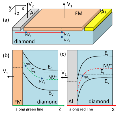
Possible means to overcome these limitations would be to apply the gate voltage in an in-plane configuration Schreyvogel et al. (2014); Shimizu et al. (2016), see Fig. 5 (b). Using aluminum (Al) as a contact, a lateral hole depletion region is formed near the Al contact with the downward band bending. An applied reverse voltage will raise the diamond Fermi level above the level, thus stabilizing shallow centers near the Al contact ( in Fig. 5 (b)).
In addition, one can use optical excitation to convert to Siyushev et al. (2013); Chen et al. (2013); Ji and Dutt (2016). The working principle is as follows. Assuming the NV center is in the neutral charge state with unoccupied level (see Fig. 2), a first laser photon will excite one electron from to , followed by another photon that excites another electron from (deep in valence band) to . The net result is the conversion of to Siyushev et al. (2013). Note that to prevent subsequent discharge of to , the laser excitation needs to be applied continuously.
III.3 Application in magnetometry
When the NVC spin is coupled to an FMH plane that hosts many spins, the exchange coupling can exist between any pair of NVC-FMH spins. However, as shown in Fig. 3, the exchange coupling quickly diminishes as the distance increases. Therefore, the exchange coupling between NVC spin and its nearest FMH spin takes the dominant role. Assuming the spin distribution in FMH layer is , and a NVC is placed at position , the total exchange energy is then , with , which means that the exchange coupling between NVC and FMH is mainly dependent on the local spin density at the NVC position.
However, the dipole field is significant even at long range, and the Zeeman splitting of the NVC ground state is induced by the combined exchange and dipole field. In contrast to the exchange field, the total dipole field induced by the FMH layer on the NV spin is the sum , where is the dipole field induced by FMH spin . The dipole field is dependent on the distance between NVC and FMH layer for a certain NVC orientation. Meanwhile, the exchange coupling is not only dependent on the NVC-FMH distance , but also on properties of the FMH/diamond junction such as barrier potential () and depletion width (), see Figs. 3 and 4. This enables us to tune the exchange coupling and the exchange field by modifying the barrier potential or depletion width, but still keeping the dipole field constant. Based on the above, we will now show that the spin distribution in FMH layer can be read out locally.
First, let us consider a specific configuration of the FMH/NVC system and then perform the ODMR measurement Jelezko et al. (2004); Childress et al. (2006); De Lange et al. (2010); Ryan et al. (2010) to determine the total Zeemann field , where . Let us assume that we can tune one of the junction properties, i.e., barrier potential or depletion width while keeping the NVC-FMH distance unchanged. Then, the exchange field is modified to be , while the dipole field is unchanged. The total Zeeman field is now . From the above, we can derive the local spin density at as follows
| (10) |
Note that Eq. (10) is obtained by assuming that the exchange coupling is only retained for the most nearest NVC spin- FMH spin pair. However, if the coupling between NVC spin and other nearby FMH spins are taken into account, Eq. (10) shall represent the average spin density in a region close to the NVC spin, which results in a lower spatial resolution. To determine the region to be averaged over, we assume that the exchange coupling can be significant between NVC spin and FMH spin separated by distance up to , where is the decay constant (see inset of Fig. 3). The intersection of the sphere centered at the origin with radius and the FMH plane is the region that will be averaged over, which is a circle of diameter . For nm and calculated value of as shown in Fig. 3, the spatial resolution is estimated to be of the range of 0.8-2 nm. For comparison, the spatial resolution in recent NV-based magnetometry experiment is up to the order of 100 nm Hingant et al. (2015).
IV CONCLUSION
We have proposed a novel FMH-NVC system engineered for observation of exchange effects between FMH spins and the NVC spin. We showed that the exchange energy can be substantial, and even surpass the usual magnetic dipole energy for low barrier heights and nanometer separation between the NVC and FMH spins, which is within the capability of present-day nanofabrication technology. This opens up possibilities to characterize FMH spintronic systems with nanometer spatial resolution and high spectroscopic precision using NV magnetometry.
Acknowledgements.
This work is supported by the Singapore National Research Foundation under Grants: NRF-NRFF2011-07, NRF-CRP14-2014-04, and CRP Programs “Next Generation Spin Torque Memories: From Fundamental Physics to Applications” NRF-CRP12-2013-01 and “Non-Volatile Magnetic Logic and Memory Integrated Circuit Devices” NRF-CRP9-2011-01, as well as the Singapore Ministry of Education Academic Research Fund Tier 1 Project R-263-000-C06-112, and Tier 2 project MOE2013-T2-2-125 (NUS Grant No. R-263-000-B10-112).Appendix A Decaying wavefunction of electron in FMH/diamond structure
The Schottky barrier can be approximated as a linearly decreasing barrier potential
| (11) |
where is the Schottky barrier height at the FMH/diamond interface, is the the conduction band minimum (CBM) of the diamond, is the depletion width. In diamond doped with nitrogen (), the depletion width is determined by , where eV is the intrinsic build-in potential Sun and Ang (2012), is applied voltage, is the dielectric constant of diamond, and is the vacuum permittivity.
Now we consider the transport of electron from FMH to the diamond. The overall wavefunction of electron can be found by solving the Schrodinger equation, which is given by
| (12) |
where
| (13) |
in which is the thickness of the FMH. In FMH region, the electron can be described by wavefunction of free electron:
| (14) |
such that the wavefunction at FMH/vacuum interface is zero, i.e., , with is a constant, and . In the diamond region, the wavefunction decays as
| (15) |
where is decay function of . In WKB formalism, the decay function is expressed as
| (16) |
Substituting the barrier potential we have:
| (17) |
The decay wavefunction is illustrated in Fig. 6. Note that with the coordinate origin at the vacancy (V), the above wavefunctions are reparameterized as , where is the FMH/NVC separation distance. The wavefunction penetration is generally enhanced for lower barrier height and smaller depletion width. As shown in previous works Gali et al. (2008); Hossain et al. (2008), the extent of the of NVC wavefunction is less than 1 nm, which is much less than the depletion width ( nm), i.e., . The decay wavefunction in Eq. (15) is approximated as
| (18) |
where , and we have assumed , with being the FM Fermi energy. From Eq. (18) we can obtain the dependence of the exchange coupling on the FMH/NVC distance and other parameters, i.e., barrier height and depletion width. First, the exchange coupling would exponentially decay as with increasing , where the decay constant is scaled with the barrier height . Second, the depletion width contributes a correction of to the decay function, which is insignificant if . Thus, the strength of the exchange coupling is a weaker function of the depletion width compared to that of the Schottky barrier height.
To obtain the normalization constants, we apply the boundary conditions at the vacuum/FMH interface and FMH/diamond interface, respectively:
| (19) |
or
| (24) |
with being the linear coefficients of deduced from Eq. 19. From this set of equations, we can find the possible energy levels by solving equation . Once the energy is found, the normalization constants and can be obtained from the normalization condition .
Appendix B hybridization
The hybridized wavefunctions of the electrons are given by
where and are the wavefunction of 2s and 2p orbital states. If we set the coordinates system so that the origin is at the vacancy (V), the N atom is on the -axis and one of the carbon atom is in plane, then wavefunctions are to be re-parameterized as , where , , , representing the relative position of the nitrogen and carbon atoms, with nm being the bond length of the diamond lattice.
References
- Jungwirth et al. (2012) T. Jungwirth, J. Wunderlich, and K. Olejnik, Nat. Mater. 11, 382 (2012).
- Wunderlich et al. (2009) J. Wunderlich, A. Irvine, J. Sinova, B. Park, L. Zârbo, X. Xu, B. Kaestner, V. Novák, and T. Jungwirth, Nat. Phys. 5, 675 (2009).
- Wunderlich et al. (2010) J. Wunderlich, B.-G. Park, A. C. Irvine, L. P. Zârbo, E. Rozkotová, P. Nemec, V. Novák, J. Sinova, and T. Jungwirth, Science 330, 1801 (2010).
- Seki et al. (2008) T. Seki, Y. Hasegawa, S. Mitani, S. Takahashi, H. Imamura, S. Maekawa, J. Nitta, and K. Takanashi, Nat. Mater. 7, 125 (2008).
- Mihajlović et al. (2009) G. Mihajlović, J. Pearson, M. Garcia, S. Bader, and A. Hoffmann, Phys. Rev. Lett. 103, 166601 (2009).
- Jalil and Tan (2014) M. B. A. Jalil and S. G. Tan, Sci. Rep. 4, 5123 (2014).
- Kent and Worledge (2015) A. D. Kent and D. C. Worledge, Nat. Nanotechnol. 10, 187 (2015).
- Matsukura et al. (2015) F. Matsukura, Y. Tokura, and H. Ohno, Nat Nano 10, 209 (2015).
- Ni et al. (2016) Y. Ni, Z. Zhang, I. C. Nlebedim, and D. Jiles, IEEE Transactions on Magnetics 52, 1 (2016).
- Kato et al. (2004) Y. Kato, R. Myers, A. Gossard, and D. Awschalom, Science 306, 1910 (2004).
- Vernier et al. (2014) N. Vernier, J.-P. Adam, S. Eimer, G. Agnus, T. Devolder, T. Hauet, B. Ocker, F. Garcia, and D. Ravelosona, Appl. Phys. Lett. 104, 122404 (2014).
- Liu et al. (2016) C. Liu, S. J. Patel, T. A. Peterson, C. C. Geppert, K. D. Christie, G. Stecklein, C. J. Palmstrøm, and P. A. Crowell, Nat. Commun. 7 (2016).
- Lou et al. (2006) X. Lou, C. Adelmann, M. Furis, S. Crooker, C. Palmstrøm, and P. Crowell, Phys. Rev. Lett. 96, 176603 (2006).
- Lou et al. (2007) X. Lou, C. Adelmann, S. A. Crooker, E. S. Garlid, J. Zhang, K. M. Reddy, S. D. Flexner, C. J. Palmstrøm, and P. A. Crowell, Nat. Phys. 3, 197 (2007).
- Martin and Wickramasinghe (1987) Y. Martin and H. K. Wickramasinghe, Appl. Phys. Lett. 50, 1455 (1987).
- Taylor et al. (2008a) J. M. Taylor, P. Cappellaro, L. Childress, L. Jiang, D. Budker, P. R. Hemmer, A. Yacoby, R. Walsworth, and M. D. Lukin, Nat. Phys. 4, 810 (2008a).
- Van der Sar et al. (2015) T. Van der Sar, F. Casola, R. Walsworth, and A. Yacoby, Nat. Commun. 6 (2015).
- Arai et al. (2015) K. Arai, C. Belthangady, H. Zhang, N. Bar-Gill, S. DeVience, P. Cappellaro, A. Yacoby, and R. L. Walsworth, Nat. Nanotechnol. (2015).
- Rugar et al. (2015) D. Rugar, H. J. Mamin, M. H. Sherwood, M. Kim, C. T. Rettner, K. Ohno, and D. D. Awschalom, Nat. Nanotechnol. 10, 120 (2015).
- DeVience et al. (2015) S. J. DeVience, L. M. Pham, I. Lovchinsky, A. O. Sushkov, N. Bar-Gill, C. Belthangady, F. Casola, M. Corbett, H. Zhang, M. Lukin, et al., Nat. Nanotechnol. 10, 129 (2015).
- Grinolds et al. (2014) M. Grinolds, M. Warner, K. De Greve, Y. Dovzhenko, L. Thiel, R. L. Walsworth, S. Hong, P. Maletinsky, and A. Yacoby, Nat. Nanotechnol. 9, 279 (2014).
- Degen (2008) C. L. Degen, Appl. Phys. Lett. 92, 243111 (2008).
- Manson et al. (2006) N. Manson, J. Harrison, and M. Sellars, Phys. Rev. B 74, 104303 (2006).
- Acosta and Hemmer (2013) V. Acosta and P. Hemmer, MRS Bull. 38, 127 (2013).
- Hingant et al. (2015) T. Hingant, J.-P. Tetienne, L. J. Martínez, K. Garcia, D. Ravelosona, J.-F. Roch, and V. Jacques, Phys. Rev. Applied 4, 014003 (2015).
- Ofori-Okai et al. (2012) B. Ofori-Okai, S. Pezzagna, K. Chang, M. Loretz, R. Schirhagl, Y. Tao, B. Moores, K. Groot-Berning, J. Meijer, and C. Degen, Phys. Rev. B 86, 081406 (2012).
- Naydenov et al. (2010) B. Naydenov, F. Reinhard, A. Lämmle, V. Richter, R. Kalish, U. F. S. D’Haenens-Johansson, M. Newton, F. Jelezko, and J. Wrachtrup, Appl. Phys. Lett. 97, 242511 (2010).
- Schwartz et al. (2014) J. Schwartz, S. Aloni, D. F. Ogletree, M. Tomut, M. Bender, D. Severin, C. Trautmann, I. W. Rangelow, and T. Schenkel, J. Appl. Phys. 116, 214107 (2014).
- Ohno et al. (2012) K. Ohno, F. Joseph Heremans, L. C. Bassett, B. A. Myers, D. M. Toyli, A. C. Bleszynski Jayich, C. J. Palmstrøm, and D. D. Awschalom, Appl. Phys. Lett. 101, 082413 (2012).
- Rondin et al. (2014) L. Rondin, J. Tetienne, T. Hingant, J. Roch, P. Maletinsky, and V. Jacques, Rep. Prog. Phys. 77, 056503 (2014).
- Balasubramanian et al. (2008) G. Balasubramanian, I. Chan, R. Kolesov, M. Al-Hmoud, J. Tisler, C. Shin, C. Kim, A. Wojcik, P. R. Hemmer, and A. Krueger, Nature 455, 648 (2008).
- Taylor et al. (2008b) J. Taylor, P. Cappellaro, L. Childress, L. Jiang, D. Budker, P. Hemmer, A. Yacoby, R. Walsworth, and M. Lukin, Nat. Phys. 4, 810 (2008b).
- Jelezko et al. (2004) F. Jelezko, T. Gaebel, I. Popa, A. Gruber, and J. Wrachtrup, Phys. Rev. Lett. 92, 076401 (2004).
- Childress et al. (2006) L. Childress, M. G. Dutt, J. Taylor, A. Zibrov, F. Jelezko, J. Wrachtrup, P. Hemmer, and M. Lukin, Science 314, 281 (2006).
- De Lange et al. (2010) G. De Lange, Z. Wang, D. Riste, V. Dobrovitski, and R. Hanson, Science 330, 60 (2010).
- Ryan et al. (2010) C. Ryan, J. Hodges, and D. Cory, Phys. Rev. Lett. 105, 200402 (2010).
- Tisler et al. (2011) J. Tisler, R. Reuter, A. Lämmle, F. Jelezko, G. Balasubramanian, P. R. Hemmer, F. Reinhard, and J. Wrachtrup, ACS Nano 5, 7893 (2011).
- Mochalin et al. (2012) V. N. Mochalin, O. Shenderova, D. Ho, and Y. Gogotsi, Nat. Nanotechnol. 7, 11 (2012).
- Gong et al. (2016) J. Gong, N. Steinsultz, and M. Ouyang, Nat. Commun. 7, 11820 (2016).
- Loretz et al. (2014) M. Loretz, S. Pezzagna, J. Meijer, and C. Degen, Appl. Phys. Lett. 104, 033102 (2014).
- Acosta et al. (2009) V. Acosta, E. Bauch, M. Ledbetter, C. Santori, K.-M. Fu, P. Barclay, R. Beausoleil, H. Linget, J. Roch, and F. Treussart, Phys. Rev. B 80, 115202 (2009).
- Kaiser et al. (2007) U. Kaiser, A. Schwarz, and R. Wiesendanger, Nature 446, 522 (2007).
- Pielmeier and Giessibl (2013) F. Pielmeier and F. J. Giessibl, Phys. Rev. Lett. 110, 266101 (2013).
- Granovskij et al. (2014) M. Granovskij, A. Schrön, and F. Bechstedt, New J. Phys. 16, 023020 (2014).
- Doherty et al. (2012) M. Doherty, F. Dolde, H. Fedder, F. Jelezko, J. Wrachtrup, N. Manson, and L. Hollenberg, Phys. Rev. B 85, 205203 (2012).
- Hossain et al. (2008) F. M. Hossain, M. W. Doherty, H. F. Wilson, and L. C. L. Hollenberg, Phys. Rev. Lett. 101, 226403 (2008).
- Gali et al. (2008) A. Gali, M. Fyta, and E. Kaxiras, Phys. Rev. B 77, 155206 (2008).
- Sun and Ang (2012) S. Sun and L. Ang, J. App. Phys. 112, 066102 (2012).
- Grotz et al. (2012) B. Grotz, M. V. Hauf, M. Dankerl, B. Naydenov, S. Pezzagna, J. Meijer, F. Jelezko, J. Wrachtrup, M. Stutzmann, F. Reinhard, et al., Nat. Commun. 3, 729 (2012).
- Maier et al. (2001) F. Maier, J. Ristein, and L. Ley, Phys. Rev. B 64, 165411 (2001).
- Tiwari et al. (2011) A. K. Tiwari, J. Goss, P. Briddon, N. G. Wright, A. B. Horsfall, R. Jones, H. Pinto, and M. Rayson, Phys. Rev. B 84, 245305 (2011).
- Rietwyk et al. (2013) K. J. Rietwyk, S. Wong, L. Cao, K. O’Donnell, L. Ley, A. Wee, and C. Pakes, Appl. Phys. Lett. 102, 091604 (2013).
- Geis et al. (1996a) M. W. Geis, J. C. Twichell, and T. M. Lyszczarz, J. Vac. Sci. Technol. B 14, 2060 (1996a).
- Geis et al. (1996b) M. W. Geis, J. C. Twichell, N. N. Efremow, K. Krohn, and T. M. Lyszczarz, Appl. Phys. Lett. 68, 2294 (1996b).
- Santori et al. (2009) C. Santori, P. E. Barclay, K.-M. C. Fu, and R. G. Beausoleil, Phys. Rev. B 79, 125313 (2009).
- Collins (2002) A. T. Collins, Journal of Physics: Condensed Matter 14, 3743 (2002).
- Farrer (1969) R. Farrer, Solid State Commun. 7, 685 (1969).
- Weber et al. (2010) J. Weber, W. Koehl, J. Varley, A. Janotti, B. Buckley, C. Van de Walle, and D. D. Awschalom, PNAS 107, 8513 (2010).
- Steeds et al. (2000) J. Steeds, S. Charles, J. Davies, and I. Griffin, Diamond Relat. Mater. 9, 397 (2000).
- Hauf et al. (2011) M. Hauf, B. Grotz, B. Naydenov, M. Dankerl, S. Pezzagna, J. Meijer, F. Jelezko, J. Wrachtrup, M. Stutzmann, F. Reinhard, et al., Phys. Rev. B 83, 081304 (2011).
- Schreyvogel et al. (2014) C. Schreyvogel, M. Wolfer, H. Kato, M. Schreck, and C. E. Nebel, Sci. Rep. 4 (2014).
- Doi et al. (2014) Y. Doi, T. Makino, H. Kato, D. Takeuchi, M. Ogura, H. Okushi, H. Morishita, T. Tashima, S. Miwa, S. Yamasaki, P. Neumann, J. Wrachtrup, Y. Suzuki, and N. Mizuochi, Phys. Rev. X 4, 011057 (2014).
- Karaveli et al. (2016) S. Karaveli, O. Gaathon, A. Wolcott, R. Sakakibara, O. A. Shemesh, D. S. Peterka, E. S. Boyden, J. S. Owen, R. Yuste, and D. Englund, PNAS 113, 3938 (2016).
- Maier et al. (2000) F. Maier, M. Riedel, B. Mantel, J. Ristein, and L. Ley, Phys. Rev. Lett. 85, 3472 (2000).
- Siyushev et al. (2013) P. Siyushev, H. Pinto, M. Vörös, A. Gali, F. Jelezko, and J. Wrachtrup, Phys. Rev. Lett. 110, 167402 (2013).
- Chen et al. (2013) X.-D. Chen, C.-L. Zou, F.-W. Sun, and G.-C. Guo, Appl. Phys. Lett. 103, 013112 (2013).
- Ji and Dutt (2016) P. Ji and M. V. G. Dutt, Phys. Rev. B 94, 024101 (2016).
- Fu et al. (2010) K.-M. Fu, C. Santori, P. Barclay, and R. Beausoleil, Appl. Phys. Lett. 96, 121907 (2010).
- Doi et al. (2016) Y. Doi, T. Fukui, H. Kato, T. Makino, S. Yamasaki, T. Tashima, H. Morishita, S. Miwa, F. Jelezko, Y. Suzuki, et al., Phys. Rev. B 93, 081203 (2016).
- Katagiri et al. (2004) M. Katagiri, J. Isoya, S. Koizumi, and H. Kanda, Appl. Phys. Lett. 85, 6365 (2004).
- Van Wyk et al. (1997) J. Van Wyk, E. Reynhardt, G. High, and I. Kiflawi, J. Phys. D: Appl. Phys. 30, 1790 (1997).
- Tallaire et al. (2006) A. Tallaire, A. Collins, D. Charles, J. Achard, R. Sussmann, A. Gicquel, M. Newton, A. Edmonds, and R. Cruddace, Diamond Relat. Mater. 15, 1700 (2006).
- Shimizu et al. (2016) M. Shimizu, T. Makino, T. Iwasaki, J. Hasegawa, K. Tahara, W. Naruki, H. Kato, S. Yamasaki, and M. Hatano, Diamond Relat. Mater. 63, 192 (2016).