Enhancement of Terahertz Photoconductive Antennas and Photomixers Operation by Optical Nanoantennas
Abstract
Photoconductive antennas and photomixers are very promising sources of terahertz radiation that is widely used for spectroscopy, characterisation and imaging of biological objects, deep space studies, scanning of surfaces and detection of potentially hazardous substances. These antennas are compact and allow generation of both ultrabroadband pulse and tunable continuous wave terahertz signal at room temperatures, without a need of high-power optical sources. However, such antennas have relatively low energy conversion efficiency of femtosecond laser pulses or two close pump wavelengths (photomixer) into the pulsed and continuous terahertz radiation, correspondingly. Recently, an approach to solving this problem has been proposed, that involves known methods of nanophotonics applied to terahertz photoconductive antennas and photomixers. This approach comprises the use of optical nanoantennas for enhancing the efficiency of pump laser radiation absorption in the antenna gap, reducing the lifetime of photoexcited carriers, and improving antenna thermal efficiency. This Review is intended to systematise all the results obtained by researchers in this promising field of hybrid optical-to-terahertz photoconductive antennas and photomixers.
Introduction
Terahertz (THz) range of electromagnetic waves tightly seated between microwave and optical regions, is of great interest, primarily due to the fact that in this band of the electromagnetic spectrum reside frequencies of some elementary excitations in semiconductors and dielectrics Ferguson and Zhang (2002); Schmuttenmaer (2004); Tonouchi (2007); Jepsen et al. (2011); Pereira (2014); Xie et al. (2013); Wharmby and Bagley (2015); Ozyuzer et al. (2007); Welp et al. (2013); Kashiwagi et al. (2011), as well as rotational and vibrational spectra of complex, including biological, molecules Zeitler et al. (2007); Jin et al. (2006); Globus et al. (2003); Cunningham et al. (2011); Parrott and Zeitler (2015); Niessen et al. (2013, 2015); Falconer and Markelz (2012); Murakami et al. (2012). As a result, THz waves have tremendous application capacity in areas ranging from the detection of dangerous and illicit substances Federici et al. (2005); Corsi and Sizov (2014); Pereira and Shulika (2014); Xin et al. (2014); Jepsen et al. (2011); Zeitler et al. (2007) to diagnosis and treatment of diseases in medicine Davies et al. (2002); Falconer and Markelz (2012); Murakami et al. (2012); Kawase et al. (2011); Yu et al. (2012); Ashworth et al. (2009); Wallace et al. (2006); Shiraga et al. (2014); Rong et al. (2015). Moreover, this frequency band is of a special importance for spectroscopy in astrophysics Coppin et al. (2011); Wyrowski et al. (2012); Graf et al. (2015); Smirnov et al. (2012); Maezawa (2015); Rogalski and Sizov (2011) for the reason that many astrophysical objects emit in the THz range of the spectrum. In addition, THz technology is promising for wireless communication systems as a replacement for transmitters and receivers operating in high-frequency and microwave ranges, because it can potentially increase the speed of data transfer by hundreds of times Federici and Moeller (2010); Hu and Lucyszyn (2014); Koenig et al. (2013); Pan and Shi (2013); Karisan and Sertel (2013); Wang et al. (2014). Although, there are hurdles, like strong absorption of THz waves by metals and water, on the way to the replacement of mega- and gigahertz frequency devices Richardson et al. (2013); Xu et al. (2006); Siles et al. (2015), a significant progress has already been made Tonouchi (2007); Hwu et al. (2013); Ducournau et al. (2014); Seeds et al. (2015).
Until relatively recently, the generation of coherent THz waves (in other words, submillimeter radiation) was an extremely difficult task. However, research in the semiconductors Vodopyanov (2008); Saeedkia and Safavi-Naeini (2008); Pereira (2014); Xie et al. (2013); Otsuji et al. (2013); Wilke et al. (2014); Leyman et al. (2016), and the interaction of short (compared with all relaxation times) optical pulses with semiconductor and nonlinear materials (photoconductivity effect Johnston (2012); Tani et al. (2012)) stimulated the development of compact low-power THz radiation transmitters. One of the most simple but not the most efficient way to obtain the submillimeter waves is by acceleration of movement of the separated charge carriers in the surface field of a semiconductor under ultrashort light pulses Johnston (2012); Pereira (2014). One of the physical mechanisms that drives the carriers inside a semiconductor is photo-Dember effect. Photo-Dember effect is the formation of the electric field (and consequently a charge dipole) in the illuminated semiconductor due to the difference of electrons and holes diffusion velocities Apostolopoulos and Barnes (2014) under the strong absorption of optical excitation, which leads to an effective charge separation in the direction perpendicular to the semiconductor surface Johnston et al. (2002). Another possible way to generate THz – optical rectification – works when media obtains non-linear polarisation under intense optical radiation, and results in polarisation repeating the shape of the optical pulse envelope Fülöp et al. (2011); Ravi et al. (2015); Abraham et al. (2014). Moreover, apart from these well-established methods, novel approaches of photonics to THz generation that employ artificial electromagnetic medium (metamaterials and metasurfaces) have been recently proposed McCutcheon et al. (2009); Docherty and Johnston (2012); Luo et al. (2014); Polyushkin et al. (2014); Atrashchenko et al. (2014); Zhang et al. (2015); Seifert et al. (2016); Kato et al. (2016); Matsui et al. (2016).
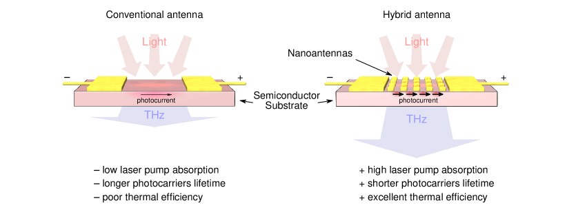
Nowadays, the most common method of low power THz generation involves the use of semiconductor structures surface conductivity Berry and Jarrahi (2012a); Berry et al. (2013a). Two or more conductive electrodes spaced by a certain gap are deposited onto semiconductor surface (Figure 1, left side). The electrodes are biased by the external voltage of several . Such structure is referred to as THz photoconductive antenna if pumped by femtosecond optical pulses, or THz photomixer in the case of continuous (CW) pump by two lasers operating at close wavelengths with a difference frequency of these wavelengths being in the THz spectral range. When exciting the gap between the electrodes with a femtosecond laser, the concentration of charge carriers increases sharply for a short period of time. At this point, THz pulse generation occurs. The duration of this pulse and its spectrum are determined mainly by the carriers lifetime in the semiconductor. In the case of CW pumping, carrier concentration changes with difference frequency of pump wavelengths, and CW THz signal is emitted. The efficiency of such THz sources is strongly limited by the amount of the optical energy of laser radiation absorbed in the gap of photoconductive antenna. Usually this amount is rather small, taking into account the high values of the semiconductor refractive index at optical frequencies, leading to a high reflection coefficient. Moreover, the effectiveness of traditional photoconductive antennas is limited by low drift velocities of the photoinduced charge carriers in semiconductor substrates Loata et al. (2007); Hattori et al. (2006); Piao et al. (2000).
It has been shown recently, that the efficiency of a THz pulse generation can be significantly increased by placing the so-called optical nanoantennas Crozier et al. (2003); Biagioni et al. (2012); Krasnok et al. (2013); Bharadwaj et al. (2009); Ni et al. (2012); Miroshnichenko et al. (2011); Park et al. (2012a); Patel and Argyropoulos (2015); Novotny and van Hulst (2011); Krasnok et al. (2015a) into the photoconductive gap (Figure 1, right side) Jarrahi (2015a); Berry et al. (2014a, 2013b); Berry and Jarrahi (2012a); Berry et al. (2013a, 2014b, 2014c); Jooshesh et al. (2014); Yang et al. (2014). As a result of such integration, one gets an antenna comprising a comprehensive photoconductive THz antenna, and an array of optical nanoantennas (see Figure 1). Such antenna can be called a hybrid THz-optical photoconductive antenna. These antennas are the result of application of known methods of nanophotonics to the area of efficient sources of THz radiation. The efficiency of the entire hybrid antenna is determined by the efficiencies of THz photoconductive antenna and an optical nanoantenna array, and is usually higher by at least one order of magnitude. Moreover, optical nanoantennas embedded in a THz photoconductive antenna improve a thermal stability of the latter, due to the large thermal conductivity of metals which they are made of. As for detectors, the use of hybrid photoconductive THz detectors, with nanoparticles in the photoconductive gap, allowed the enhancement of the near field THz imaging resolution down to Mitrofanov et al. (2015). Such hybrid THz-optical antennas will be discussed in this Review.
It should be noted that the present Review is the first attempt to collect all currently available literature about hybrid THz-optical antennas. The aim of this Review is to demonstrate recent achievements in this field. We will not focus on the current research in the field of conventional photoconductive antennas and photomixers, but will briefly describe their main operating principles. A great number of excellent reviews have been written on this subject, among them we strongly recommend the following Jepsen et al. (2011); Krishna et al. (2012); Winnerl (2012); Federici and Moeller (2010); Reimann (2007); Vodopyanov (2008). Our Review is primarily addressed to specialists working with THz radiation and its compact sources, but is written in such a way that both engineers and physicists working in related areas, can study the methods of THz generation using semiconductors and then obtain an information about the latest achievements in the field of hybrid photoconductive antennas.
The Review is structured as follows. In Part I the most general principles of THz generation in semiconductor sources pumped with femtosecond optical pulses and double-wavelength CW laser radiation are described: in Section I.1 the mechanisms of pulsed THz radiation generation in semiconductors are considered in more detail; Section I.2 is completely dedicated to the principles of THz photoconductive antennas; Section I.3 describes the principles of THz photomixers; Section I.4 contains the information about the main characteristics of such antennas. Part II is entirely devoted to the review of hybrid THz-optical photoconductive antennas: Section II.1 outlines the general principles of operation of optical nanoantennas and the prospects they offer; Section II.2 describes the plasmon monopoles as an effective way to enhance the conversion of light into current; Section II.3 contains a detailed description of metal dipole nanoantennas, their types and features of their operation in hybrid antennas; Section II.4 is devoted to plasmon gratings as absorption amplifiers in the gaps of the photoconductive antennas; Section II.5 reviews the works on three-dimensional plasmonic gratings. Part III is the discussion and outlook, which summarises all the results described in detail in Part II, compares all the approaches to the implementation of the hybrid antennas, and offers further perspectives of their development such as all-dielectric nanoantennas and the search for new materials.
I THz photoconductive antennas and photomixers
I.1 The mechanism of pulsed THz radiation in semiconductors
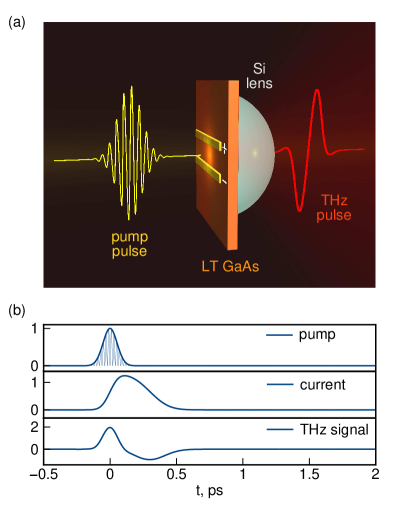
Currently, there are many different approaches to THz generation, in a vast variety of layouts and involving various materials. However, for practical applications, a method involving the excitation of non-equilibrium charge carriers in the surface layer of semiconductor structures by ultrashort optical pulses is the most widely used now. Figure 2(a) shows the simplest layout for sub-millimetre waves generation in semiconductor based photoconductive antenna. Femtosecond laser (usually Ti:Sapphire or fibre Jepsen et al. (2011)) serves as a source of ultrashort light pulses with a duration of several tens or hundreds of femtoseconds. The shape of the optical pulse envelope is important, as it induces the nonlinear polarization of the same shape therein (optical rectification), which is capable to increase the output power of THz radiation Fülöp et al. (2011); Ravi et al. (2015). Silicon lens, shown in Figure 2(a), serves as a collecting lens for THz radiation Sherry et al. (2011); Van Rudd and Mittleman (2002) and at the same time as a heatsink to transfer an excess of heat from the substrate, and as an anti-reflective element, since the refractive index of silicon in THz is equal to Grischkowsky et al. (1990), which is about the same as one of high-resistive GaAs () Grischkowsky et al. (1990).
Let us consider the model of THz generation in a semiconductor. The dependence of the output power on the frequency is as follows Gregory et al. (2005):
| (1) |
where is the effective lifetime of photocarriers, equal to the lifetime of nonequilibrium charge carriers in the semiconductor. From the equation (1), it is clearly seen that the shorter the lifetime is, the greater power can be obtained. Therefore, gallium arsenide grown by molecular beam epitaxy on a low-temperature (LT) substrate (LT-GaAs) is usually chosen as a photoconductive material, as this growth method allows to obtain a material with more defects and hence with a shorter lifetimes of nonequilibrium charge carriers ( 200 fs Gregory et al. (2005)). When irradiated by femtosecond laser pulses with photon energies greater than the bandgap, the concentration of nonequilibrium charge carriers in LT-GaAs rapidly increases, and in the surface layer electron-hole pairs are formed. In the semiconductor model all electrons are set to have the same effective mass, as they have a low energy because of the wide band of gallium arsenide. The model is not applicable to narrow-gap semiconductors like indium arsenide (InAs). In the case of InAs, it is necessary to consider ensembles of equilibrium and photoexcited electrons interacting through self-consistent field Malevich (2003), which greatly complicates the numerical modeling and description of processes.
Due to the localisation of charges at surface states in the surface layer, so-called built-in field appears. The light induced electrons and holes are accelerated and separated by this field. The resulting uneven distribution of charge is considered as a dipole with dipole moment equal to the sum of momenta of all induced charges in the volume. Dipole oscillations occur until the equilibrium is established again. During the relaxation, electrons emit energy in the form of electromagnetic waves in the THz range, and the relaxation time determines both the spectrum of this radiation and its power. Built-in surface field plays a very important role in this process. The stronger this field is, the more intensive THz signal is emitted. Therefore, metal electrodes are often applied to the semiconductor surface and biased to create stronger electric field. The mechanism of THz generation enhancement by such structures will be described in detail in the next section of this Review. Due to the fact that the generation takes place near the air-semiconductor interface, a larger portion of the THz radiation is emitted into the GaAs substrate. The reason for this is the greater optical density of the GaAs in comparison with air. Therefore, highly doped semiconductor materials are not suitable for efficient photoconductive antennas due to significant absorption in the THz region of the spectrum Grischkowsky et al. (1990). On the other hand, the doping of the sample increases the concentration of photoinduced electron-hole pairs, which, ultimately, increases the current and hence THz radiation power. A reasonable compromise between these factors (i.e. higher absorption vs higher current) will substantially improve the efficiency of generation.
Another effective method of increasing the efficiency of generation is the application of an external magnetic field. It has been shown, that a semiconductor placed in a constant magnetic field of 1 T generates THz radiation with efficiency up to 20 times larger than without magnetic field Nazarov et al. (2010). Magnetic field optimal direction is the one perpendicular to the semiconductor surface, and THz pulse amplitude is proportional to the magnetic field squared. This effect is explained by the appearance of the Hall component of the current, excited carriers being driven by external or surface field Zhang et al. (1993); Malevich (2003); Bespalov et al. (2002). The analysis of temperature dependence of submillimeter radiation power shows that with decreasing temperature the power goes up. With the GaAs temperature decreasing from 280 K down to 80 K, the radiation energy is increased by 3.4 times Zhang and Auston (1992).
I.2 Pulse THz generation in photoconductive antennas
A way of THz generation in a semiconductor surface by the accelerated motion of nonequilibrium charge carriers driven by semiconductor surface field and induced by femtosecond laser pulses, has, however, low optical-to-terahertz conversion efficiency. Therefore, metal electrodes (usually a nickel-gold-platinum alloy) are deposited onto the substrate surface and are biased to create high electric field in in the gap between them, where photocarriers are generated, and thus enhance the generation of the THz waves Auston et al. (1984). Such structures together with a photoconductive semiconductor substrate are referred to as THz photoconductive antennas. An example and principle of operation of such antenna is shown in Figure 2(a).
The mechanism of THz generation in this case is similar to that discussed in the preceding section. Under the ultrashort laser pulse, electron-hole pairs are formed in the surface layer. The conductivity of the semiconductor as a consequence greatly increases proportional to electrons and holes concentration: , where q is the elementary charge, and are the concentrations of electrons and holes, and are their mobilities. The increase of conductivity results in a giant current pulse of photoinduced charges, electrons and holes being accelerated in opposite directions by the external electric field in the gap. The acceleration of charge carriers by the external field in this case can be described by the differential equation:
| (2) |
where is the drift velocity of electrons and holes, are their masses, is approximately 30 fs in low-temperature GaAs, is a local field, which is related to with the following ratio: , where is the static dielectric susceptibility of semiconductor (equal to 3 for the LT-GaAs), is the vacuum permittivity, is the polarization caused by the separation of electrons and holes. The time evolution of polarization can be described by the following inhomogeneous differential equation:
| (3) |
where is the recombination time of holes and electrons, and is the density of currents on the surface of the semiconductor defined by: . From expressions (2-3), using Maxwell’s equations, the authors of the article Chang et al. (2005) derived a formula for the intensity of the radiated THz field at a much larger than THz wavelength distance z from the source:
| (4) |
where is the total concentration of carriers, is their velocity, is the area of radiating surface, equal to the area of the gap between the electrodes, and is the speed of light in vacuum. Thus, the external field increases the energy of charge carriers, and hence the output power of THz radiation, not influencing, however, the spectral characteristics, as it is determined by the lifetime of electrons and holes. Pump pulse envelope, photocurrent in the surface layer and resulting THz field examples obtained with this model are shown in Figure 2(b).
Authors of Ref. Berry and Jarrahi (2012b) have observed that various pump of the semiconductor in the THz photoconductive antenna gap can affect the output power. Moreover, there are two options for photoconductor pump: uniform illumination of the antenna gap, and partial and asymmetric illumination of the gap close to the anode (Figure 3(a)). In the case of uniform illumination, the current of photoinduced charge carriers is directly proportional to the optical power of the pump. However, in the case of asymmetric illumination, photocurrent and hence THz signal are nonlinearly proportional to the optical pump power. This pumping regime is characterised by the increased electric field near the anode, and, consequently, increased electrons concentration in this region (Figure 3(b)). This leads to an increase of the photocurrent, resulting in an increased THz signal power. According to Ref. Berry and Jarrahi (2012b), the asymmetric illumination of the photoconductive antenna gap gives more than 4-fold enhancement compared to the uniform illumination. Moreover, it has been shown that the stronger optical field is focused in the area of the anode, the more powerful THz radiation is Ralph and Grischkowsky (1991).
I.3 Continuous THz generation in photomixers
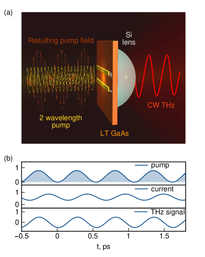
The process of THz heterodyne generation in semiconductors is similar to that discussed in the preceding sections, with the only difference being the pump laser regime. Under the continuous double-wavelength pump with a frequency difference lying in the THz region, electron-hole pairs are formed in the surface layer and the conductivity of the semiconductor is modulated proportionally to the electrons and holes concentration, as the pump intensity beats with the frequency corresponding to the difference between two incoming optical pump frequencies. Such devices for photoconductive CW THz generation are usually called photomixers Brown et al. (1993); McIntosh et al. (1995). Schematic layout of CW THz generation in photomixer, and principle of its operation are shown in Figure 4.
Surface conductivity in photomixer and charge carriers acceleration are similar to the ones in photoconductive antenna, and the number of carrier pairs similarly follows the pump evolution:
| (5) |
where is the external quantum efficiency, is the pump intensity, is the carrier recombination time, and is the energy of the pump photon.
Pump radiation on the case of photomixing comprises two laser beams bringing to the surface average intensities and at the frequencies and , correspondingly. Thus, the intensity at the surface would be described as:
| (6) |
The second oscillating term in the sum changes within a timescale that is significantly shorter than the carrier effective recombination time , hence it won’t affect the photocurrent. Then after substitution of Eq. 6 into Eq. 5, we get the evolution of carrier density Brown et al. (1993):
| (7) |
where is the THz frequency, and in the phase delay due to the carriers lifetime.
Since the applied field is constant, for the photocurrent we obtain Lee (2009)
| (8) |
where is the DC photocurrent and is the AC part of the current, responsible for the generation of the CW THz signal:
| (9) |
It can be seen, that for the maximum conversion efficiency, the powers of both wavelength modes should be as close to each other as possible. Pump intensity profile, corresponding photocurrent and far field THz signal of the photomixer calculated with the described model are shown in Figure 4(b).
I.4 Affect of the contact shape onto THz photoconductive antenna and photomixer radiative characteristics
In a number of works Mendis et al. (2005); Berry et al. (2014a, 2013b); Jarrahi (2015b); Maraghechi and Elezzabi (2010) it was observed that the geometry of the electrodes affects both the width of the spectrum and the position of the maximum of the radiation intensity in the far field, as well as its intensity value. Comparative analysis of different geometries was done as well. For THz antennas, the same geometries as in their RF and microwave counterparts are used: dipole, logarithmic, spiral antenna, bow-tie Rebeiz (1992); Brown et al. (2006); Matsuura et al. (1997); Tani et al. (1997).
One of the most important characteristics of all antennas, including traditional radio, microwave and THz photoconductive, is the amount of the emitted power. However, between the traditional and THz antennas there is one significant difference – the nature of the input signal. In the case of a THz antenna it is the laser radiation that generates the nonequilibrium electrons and holes photocurrent in the surface layer of the photoconductor. Therefore, the THz photoconductive antenna, or photomixer are usually considered as a system consisting of two elements: the photoconductor and the antenna. These elements in turn are described in the traditional physical quantities, such as active and reactive conductivity, capacitance, and input impedance Berry and Jarrahi (2012b); Gregory et al. (2005).
The output power of THz photoconductive antenna is given by the formula Berry and Jarrahi (2012b):
| (10) |
where is the current susceptibility of the photoconductor, optical pump power at frequency , is the antenna efficiency (describes the dissipative losses in the antenna material Balanis (2005)), and are active and reactive conductances of the antenna respectively, is the conductivity of the photoconductor, and its capacitance. Regardless of the THz photoconductive antenna geometry, in order to maximise its radiated power, its stray conductance must be much less than its active conductance. Full or partial compensation of reactive conductance can be achieved by maintaining inductive load of the antenna on the same level as capacitive load of the photoconductor, or by adding a negative reactive conductance shunt into the circuit Duffy et al. (2001a); Brown (2003).
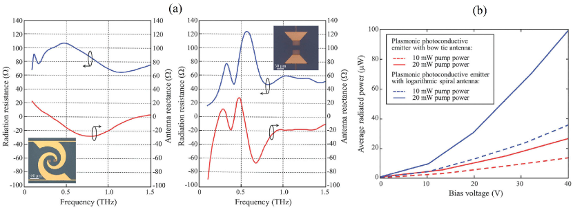
In Ref. Berry et al. (2014b) a comparative analysis of two common THz antenna geometries is performed: spiral and bow-tie. Figure 5 shows plots of the dependence of radiation resistance and reactance of these antennas on the frequency and the dependence of the radiated power on the bias applied to electrodes for THz frequency corresponding to the maximum output power (Figure 5(b)). It can be seen that the spiral antenna having larger radiation resistance and smaller reactance, emits more effectively than the bow-tie within wider range of frequencies. Thus, the maximum active resistance and the minimum absolute value of the reactive resistance are prerequisite for efficient THz radiation generation Brown et al. (2006); Ezdi et al. (2006).
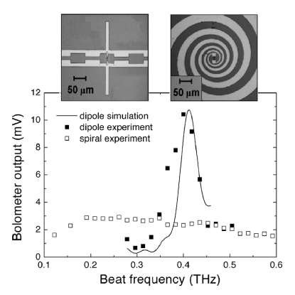
Since active and reactive resistances affect the power emitted by THz antenna, the spectral characteristics of antenna impedance and reactance determine the spectral characteristics of the THz signal. It has been observed that antenna with a radiation resistance, weakly dependent on frequency in the THz range, has a wider frequency range of effective operation Verghese et al. (1997); Berry et al. (2014b). Spiral and a bow-tie geometries are examples of such antennas. Figure 6 shows the spectrum of THz signal from the spiral photomixer antenna measured by bolometer. At frequencies between 0.1 and 0.6 THz the signal power is almost constant Gregory et al. (2005). On the other hand, antennas with a pronounced resonance characteristic impedance of, for example, full-wavelength dipole antenna have narrow-band emission spectrum (Figure 6) Duffy et al. (2001a); Gregory et al. (2004); Nguyen et al. (2011).
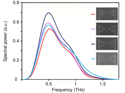
In the work Maraghechi and Elezzabi (2010) bow-tie antenna are studied, made in the form of Sierpinski triangles, the results are shown in Figure 7. After analyzing them, one can conclude that increasing the order of fractality allows gaining the power emitted by the bow-tie to the far field.
II Hybrid Photoconductive Antennae for Terahertz Generation
II.1 Principle of a hybrid THz-optical photoconductive antennas operation
Availability of powerful optical sources of ultrashort light pulses, as well as technologies of manufacturing the necessary semiconductor materials and deposition of metal structures on them makes photoconductive antennas promising sources of THz waves. However, the effectiveness of traditional photoconductive antennas is limited by low drift velocities of the photoinduced charge carriers in semiconductor substrates Loata et al. (2007); Hattori et al. (2006); Piao et al. (2000). For efficient optical-to-terahertz conversion in the frequency range above 0.5 THz a relaxation time of carriers , as discussed earlier in Section I must be subpicosecond. According to the formula:
| (11) |
the mean free path is about 100 nm. Therefore, only a small part (about 5% Berry et al. (2013a)) of nonequilibrium electrons and holes reaches the electrodes and participate in the efficient THz generation. The rest of the charge carriers recombines with charges of opposite sign on the way towards the electrodes. This effect is called carrier screening effect Loata et al. (2007); Piao et al. (2000). The diffraction limit for electromagnetic waves does not allow to focus the laser pump into the spot of 100 nm, to allow involvement of all the excited carriers. Therefore, in order to reduce the effect of screening and to improve the properties of photoconductive antennas, optical nanoantennas are used Park et al. (2012a).
Optical nanoantennas possess all the inherent characteristics of their radio and THz counterparts, except of course that they operate on electromagnetic waves with frequencies in the optical spectral range, whereby the dimensions of such antennas are typically of the order of several hundreds of nanometers. Optical nanoantennas are used extensively in devices that use photon-electron conversion, such as photodiodes, LEDs and photovoltaic converters Krasnok et al. (2013); Bharadwaj et al. (2009). Nanoantennas can be plasmonic (metal), dielectric and metal-dielectric Krasnok et al. (2013); Bharadwaj et al. (2009). The most widely used and well-studied nanoantennas are the plasmonic ones. Recently, a number of papers appeared that demonstrate the successful enhancement of optical-to-terahertz conversion as a result of the integration of such plasmonic antennas into the gap between metal electrodes of THz photoconductive antennas to enhance the absorption cross-sections of laser radiation into semiconductor substrate. Such a device (which combines optical nanoantennas and THz photoconductive antenna) is known as a hybrid optical-to-THz photoconductive antenna.
Receiver optical nanoantennas, as part of a hybrid THz-optical photoconductive antenna or photomixer, convert the pump optical radiation into a strong near field and redistribute energy into the semiconductor surface layer. Local electric field enhancement is described by the local field enhancement factor:
| (12) |
This value shows what fold increase gets the module of the electric field at the point in the presence of the nanoantenna compared to the one without nanoantenna .
Local electric field enhancement occurs due to the structure plasmon resonance Brongersma and Kik (2007); Berry et al. (2013b); Berry and Jarrahi (2012a). At the same time, surface plasmon excited in the metal structure asymmetrically scatters the incident wave, and the field is redistributed in the semiconductor substrate so that the local electric field enhancement factor near the electrodes becomes much greater than 1. Therefore, the optical power absorbed by the semiconductor in the volume :
| (13) |
increases proportionally . Because of this, the concentration of nonequilibrium charge carriers near the electrodes increases, and, according to the dependence:
| (14) |
where is the amplitude of the output THz signal, is the process duration, the efficiency of optical-to-terahertz conversion increases. It is important to note that physical dimensions of the nanoantennas and the material they are made of play an important role in the excitation of plasmon resonance.
Moreover, optical nanoantennas embedded in a THz photoconductive antenna, improve thermal stability of the latter, due to the large thermal conductivity of gold, which they are made of Jooshesh et al. (2014). The excess of heat in traditional THz antennas leads to the thermal generation of carriers after optical pulse excitation. Recombination of thermal and photoinduced carriers in subsequent cycles of charge carriers generation prevents the stable operation of the photoconductive antenna. Thus, higher thermal efficiency also makes optical nanoantennas attractive for use in THz sources.
Thus, the design of optical nanoantennas embedded in a THz photoconductive antenna should maximize the transfer of light energy into the absorptive semiconductor substrate and minimize the path length of charge carriers traveling between metallic electrodes. Here, we review the most recent works and organise them according to the approach to optical nanoantenna realisation.
II.2 Plasmon Monopoles
The simplest approach to realisation of optical nanoantennas is monopole nanoantennas. Monopole nanoantennas are able to provide strong localisation of laser radiation power near them Krasnok et al. (2013). The characteristics of such antennas are highly dependent on the size and material of the nanoparticle, but still have the least number of tunable parameters and are therefore particularly important for applications that require the large nanoantenna array, for example in the gap of the THz photoconductive antenna.
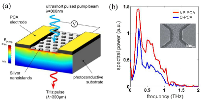
The authors of Park et al. (2012b) propose silver plasmonic monopole nanoantennas in the form of so-called nanoislands (Figure 8(a)). The fabrication of such monopole nanoantennas is done by thermal evaporation of silver (Ag), with subsequent deposition onto LT-GaAs antenna substrate surface. This method can be used to pattern nanostructures inside a large area, because of lower costs if compared to, for example, electron beam lithography used for the precise fabrication of metal nanostructures Oh and Jeong (2012). Silver in the hybrid THz-optical antenna is used due to the high quality factor of the silver nanostructures in the visible range, which allows achieving maximum localization of the field in the semiconductor surface layer in close proximity to a nanoantenna, with minimal losses. In addition, Ag has a relatively low melting temperature, and therefore its thermal evaporation is possible without thermal damage to the semiconductor GaAs substrate Vogt and Kohl (1993). The geometrical parameters of the monopoles are specially derived so that surface plasmon waves are excited in the structure under an optical pump. For a pump radiation of 800 nm wavelength, which is typical for Ti:Sapphire femtosecond lasers, nanoislands should have a thickness of 20 nm and a diameter of 173 nm.
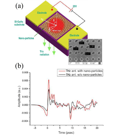
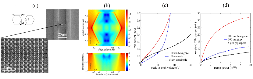
Figure 8(b) shows the comparative characteristics of traditional (C-PCA) and nanoisland improved (NP-PCA) THz photoconductive antenna. It is clearly seen that the hybrid structure has 1.5-2 times higher conversion efficiency, and particularly enhances high-frequency part of the generated spectrum. This advantage is explained by the following dependence (Eq. 14): monopole nanoantenna concentrate the light inside the gaps between adjacent nanoparticles, so that the absorption of optical radiation in these areas increases, hence grows the concentration of nonequilibrium carriers , which, ultimately, increases the amplitude of the output THz signal . However, this field redistribution leads to a decrease in its value under nanoislands and significantly reduces the density of electrons and holes in these areas. However, this does not affect the total current of photoinduced charges, as silver monopoles are almost perfect conductors of an external electric field. This process is described in detail in the following works: Park et al. (2012b, a).
Another possible realization is the array of rectangular monopole nanoantennas inside the photoconductive gap of the photoconductive antennas and photomixers Surdi et al. (2013). Figure 9(a) schematically shows a THz antenna with array of rectangular nanostructures and SEM image of these nanostructures. The mechanism of optical field local enhancement in these nanoantennas is similar to the one in previously described - plasmon resonance excitation. Metal deposition followed by electron beam lithography is used for the fabrication of such monopole nanoantennas. However, instead of Au metal nanostructures, which fabrication is a very expensive process, arrays of gold and germanium (AuGe) alloy monopoles are used, that not only greatly reduce costs but also reduce the risk of the thermal damage to SI-GaAs at thermal evaporation of the metal due to the relatively low melting temperature of AuGe. These nanostructured hybrid THz-optical photoconductive antennas are able to double the generation of THz radiation in comparison with traditional photoconductive antennas (Figure 9(b)).
Paper Jooshesh et al. (2014) describes hexagonal metal nanostructures superior to plasmonic nanorods (see below) in THz generation enhancement. Figure 10(a) shows the array of these monopole nanoantenna inside the photoconductive gap of the dipole THz PCA. Such structures are fabricated with the focused ion beam technology. It has been shown, that an important property of THz photoconductive antennas with integrated hexagonal nanoantennas is their high resistance to thermal breakdown. The increase of pumping intensity leads to an increase of photoinduced current carriers, which leads to heating of the semiconductor substrate and its thermal breakdown Singh et al. (2014); Liu et al. (2003). Figure 10(c) demonstrates the advantage of the hexagonal nanoantennas over grating nanoantennas and a traditional THz antennas. It is seen that to achieve similar photoinduced carriers current values, different antennas require application of different bias between the electrodes. Moreover, maintaining a predetermined value of the current in the structure with a hexagonal monopoles requires less external stress than in other antenna realisations. This suggests that traditional antennas and plasmonic gratings generate more heat than the hexagonal nanoantenna, and, accordingly, have a greater risk of thermal breakdown Jooshesh et al. (2014).
Similar comparison is shown in Figure 10(d), but for the THz power dependence on the average power of femtosecond pump laser. When comparing grating and hexagonal nanoantenna, the obvious superiority of the latter is clearly seen. This is due to a combination of the external field generated by the electrodes, and localisation of photoinduced charges in the proximity to the vertices of hexagons (Figure 10(b)).
II.3 Metal dipole nanoantennas
Typical representatives of both metal and dielectric nanoantennas are dipole nanoantennas Wissert et al. (2009). As the name implies, they represent a dipole structure consisting of two elongated nanoparticles. Such structures, especially metal, when exposed to an external electromagnetic field provide strong field localization in the gap between the nanoparticles, and a large value of the absorption cross section of quantum detector placed in the gap. Due to this property, the metal dipole nanoantennas are used in THz photoconductive antennas and photomixers, enhancing an optical field of pump laser and redistributing it into the surface layer of the semiconductor substrate near the electrodes.
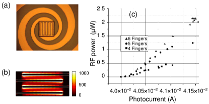
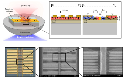
The first implementation of dipole nanoantennas embedded inside the gap of THz antenna are interdigitated nanostructured electrodes, or as they often called, ”nano-fingers” Michael et al. (2005); Hou et al. (2012); Berry et al. (2014a); Tanoto et al. (2013); McIntosh et al. (1995); Duffy et al. (2001a). Figure 11(a) presents a interdigitated nanostructures embedded in the gap between the electrodes of the logarithmic photomixer. THz photomixers with such nanostructures feature lower parasitic capacitance and, consequently, lower reactance if compared with traditional THz photomixers, as well as higher optical field localization inside the working area of the antenna (see Figure 11(b)). Hence, photomixers with nanostructured dipole antennas in the photoconductive gap are more effective sources of CW THz radiation Gregory et al. (2005) if compared to microstructured ones. In some works Mayorga et al. (2004); Mendis et al. (2004), it has been shown that with increasing number of dipoles (fingers), the optical-to-THz conversion efficiency increases (Figure 11(c)). This dependence can be explained by the smaller distance between the dipoles in THz photomixer with greater number of fingers, hence increased degree of the optical field localization in the gap and decreased effective lifetime of photoinduced charge carriers.
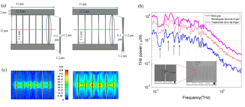
An updated approach to the design of the embedded dipole nanoantennas are the so-called dipole tip-to-tip nanoantennas Khiabani et al. (2014); Seniutinas et al. (2013); Tanoto et al. (2013). Two most commonly used realizations of such nanostructures embedded in a THz photomixer are shown above. On one side traditional rectangular dipole nanoparticles are shown and trapezoidal bow-tie nanoantennas on the other (see Figure 12(a)). Being a continuation of the metal electrodes, these tip-to-tip nanoantennas are designed to reduce the path length of photoinduced electrons and holes Wissert et al. (2009). Moreover, due to the nanoscale gap between the dipoles, tip-to-tip nanoantennas enhance the localization of the external optical field Seo et al. (2009); Tanoto et al. (2013); Seniutinas et al. (2013). High localization of the field in the gap (see Figure 12(c), left picture) occurs because of the surface plasmon excitation due to plasmon resonance at the antenna excitation wavelength Wissert et al. (2009). This increases a laser radiation absorption in the semiconductor substrate within the gap, and, consequently, the concentration of charge carriers in the gap. The rapid increase in the charge carriers concentration leads to a huge impulse of the photocurrent that is much greater than in conventional THz antennas. The amplitude of THz radiation is directly proportional to the rate of change of the photocurrent density, according to Eq. 14, so THz dipole antenna with integrated optical nanoantennas demonstrate higher output power of THz signal than traditional one at the same pump rate, only because of such nanoscale extensions of the electrodes (Figure 12(b)).
In Ref. Khiabani et al. (2014) it has been noticed, that due to lower capacitive reactive resistance, receiving ability of the bow-tie antenna is much better than one of the rectangular-shaped nanoantennas, as a result, the degree of the optical field localization in the trapezoidal nanoantenna gap is significantly higher (Figure 12 (c), right picture) Khiabani et al. (2014). In addition, a smaller capacitance increases the efficiency of generation of THz radiation by such antenna. Gregory et al. (2005).
II.4 Two-dimensional plasmonic gratings
Numerous researchers Park et al. (2012a); Berry et al. (2013a, 2014b); Jarrahi (2015b); Berry et al. (2013b, 2014c, 2014a); Jarrahi (2015a) have shown that on of the most effective implementation of dipole nanoantennas in the THz photoconductive antennas and photomixers are arrays of metal dipoles whose length is of the order of the gap size between the electrodes. Arrays of dipole plasmonic nanoantennas have received the name of plasmonic gratings or plasmonic nanorod gratings. Park et al. (2012a).
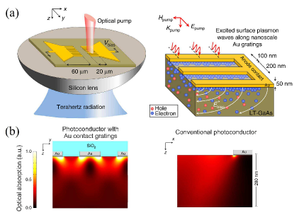
Figure 13(a) shows the bow-tie THz photoconductive antenna with embedded plasmonic gratings. Usually the penetration of light through the apertures is limited by the diffraction limit. However, the geometrical parameters of the gratings can be chosen so that the radiation of a femtosecond laser with a wavelength of 800 nm excites the surface plasmon wave in this periodic structure. The excitation of plasmon waves allows the transfer of the most part of optical pump energy into a semiconductor substrate Berry and Jarrahi (2010). The surface plasmon greatly enhance the intensity of the optical field near the metallic electrodes (Figure 13(b)), as a result, the path length of photoinduced electrons and holes to the anode and cathode is reduced in comparison with traditional THz antennas (Figure 2).
Plasmon resonance in this structure is very sensitive to the polarization of the incident light. When the electric field of the optical pulse is parallel to the plasmonic lattice nanorods, the reflection from the grating surface is sufficiently large. On the contrary, in the case of perpendicular orientation of the electric field vector and nanorods, maximum conversion of incident light into plasmon waves is achieved Park et al. (2012a).
Figure 14 depicts another possible implementation of plasmonic nanorod gratings embedded in dipole photoconductive THz antenna. Instead of comb-like plasmonic grating structures described above, the ends of plasmonic nanorods in this configuration are connected together, which significantly shortens the path of the charge carriers to the electrodes. Moreover, this design allows to reduce the capacitive reactance of the THz antenna that improves its emitting ability and increases antenna gain coefficient. A disadvantage of this plasmonic grating realization is that only half of nonequilibrium electrons and holes reach the electrodes within subpicosecond time. This limits the effectiveness of such structures to 50 percent Berry and Jarrahi (2012a).
In order to maintain the operation of the hybrid THz-optical photoconductive antenna without reducing its effectiveness, midway between the anode and the cathode grounding electrode is placed. This electrode is usually embedded into the semiconductor substrate and during a cycle of photoinduced charge carriers generation collects those electrons and holes that reach the electrodes, preventing their slow accumulation in the substrate. In the absence of a grounding electrode these unwanted carriers recombine with charges of opposite sign of the subsequent cycles of generation, thereby reducing the total number of particles that reach electrodes Berry and Jarrahi (2012a).
To manufacture such structures most often methods of electron-beam lithography, accompanied by the deposition of Au on LT-GaAs substrate are used. A dielectric layer covering nanoantenna reduces Fresnel reflection from its surface, thereby increasing the absorption coefficient of the optical pump into the substrate. Usually, 200 nm thick silica () is used for these purposes. This coating provides a 70% absorption of pump light into the semiconductor material.
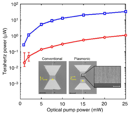
Comparison of traditional THz photoconductive antennae and hybrid optical-to-THz antennae with integrated plasmonic gratings reveals at least one order of magnitude superiority of the latter (Figure 15). Such a significant increase in the output power of THz radiation is achieved by reducing the path length of charge carriers to the electrodes, thus greatly increasing the photocurrent and decreasing the number of recombinated electron-hole pairs.
An important role in THz hybrid optical photoconductive antennas is played by the thickness of the semiconductor substrate, since at a sufficiently large depths (over 100 nm) photoinduced charge carriers begin to accumulate that do not participate in the effective generation of THz radiation. These electrons and holes rise from the depths of the substrate to the surface, where recombine with other charges, which significantly reduces the ratio of optical-terahertz conversion. To prevent negative effects caused by the non-equilibrium carriers accumulated in the lower layers of the substrate, its thickness should not exceed 100 nm. However, there is a workaround for this problem without reducing the thickness of semiconductor by using three-dimensional plasmonic gratings Yang et al. (2014).
II.5 Three-dimensional plasmonic gratings
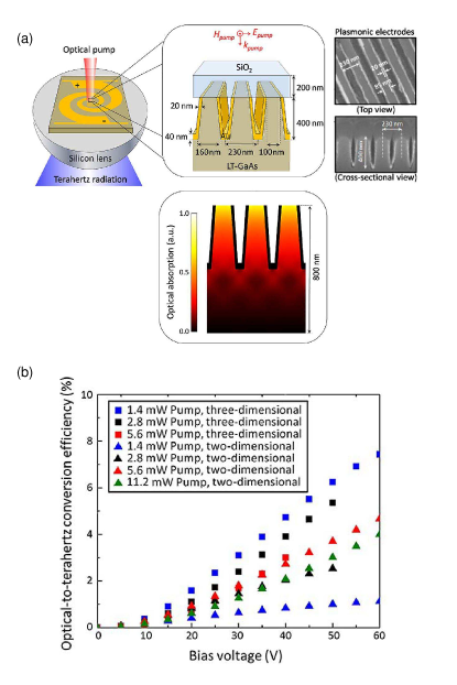
Plasmonic gratings described above are two-dimensional nano-sized structures on the semiconductor surface. They provide a high absorption of light quanta by a semiconductor material and significantly increase the concentration of photoinduced charge carriers near metal electrodes. However, the effectiveness of optical-terahertz conversion is still limited by the depth at which charge carriers are generated (100 nm). To overcome this limitation, three-dimensional plasmonic gratings embedded in the semiconductor substrate are proposed. It has been shown, that such structures allow to achieve 7.5% optical-to-THz conversion efficiency Yang et al. (2014). Figure 16 (a) shows a schematic of three-dimensional plasmonic gratings and distribution pattern of the absorbed optical radiation. Because of its complexity, the manufacturing of such antennas should be discussed in more detail. The process of three-dimensional plasmonic gratings fabrication starts with chemical vapor deposition of a 200 nm film of onto the surface of the semiconductor. Next, on the surface of the film, a nanoscale Nickel grid is applied by electron beam lithography. The grid serves as a template layer for etching of . When using reactive ion etching with a source of inductively coupled plasma a grating is formed, which serves as a mask to create nano-walls made of semiconductor material. Plasmonic grating is obtained by deposition of gold on the sidewalls of the resulting semiconductor nanostructures. The height of the walls of the nanostructure determines the order of the modes excited in the resulting subwavelength waveguides. In such a structure waveguide TEM modes of 4th order can be excited by p-component of the femtosecond laser Catrysse et al. (2006); Hsieh and Jarrahi (2011); Yang and Jarrahi (2013). A mask is then removed by wet etching. Then to reduce the losses associated with reflection, the surface of the antenna is covered with a 200 nm layer of . The resulting structure absorbs up to 70 percent of the incident laser radiation Yang and Jarrahi (2013).
Figure 16 (b) demonstrates the advantages of three-dimensional gratings two-dimensional It is seen that three-dimensional plasmonic grating has a large coefficient of optical-to-THz conversion in comparison with the two-dimensional analogue. At the optical pump power of 1.4 mW, optical-to-THz conversion efficiency reaches 7.5%. Such efficiency increase is due to the fact that three-dimensional plasmonic grating embedded into the surface layer of the semiconductor substrate, hence the contact surface of three-dimensional grating with the semiconductor is much greater than that of two-dimensional plasmonic gratings. This increases the concentration of the photoinduced charges near the metal electrodes, which are involved in the effective generation of THz radiation Yang et al. (2014). However, with increasing optical pump power, optical-to-THz conversion efficiency in three-dimensional structures decreases. This happens because large number of separated electron-hole pairs generate a significant electric field with direction opposite to the external field. The resulting field turns out to decrease, hence the efficiency of THz generation is reduced Loata et al. (2007).
Thus, the THz photoconductive antennas with integrated three-dimensional plasmonic gratings provide greater efficiency of optical-to-THz conversion in comparison with two-dimensional plasmonic gratings. In the future, despite the complexity of fabrication technology, these three-dimensional nanoscale structures can replace two-dimensional in hybrid THz-optical photoconductive antennas.
III Discussion and outlook
| Method of Plasmon Resonance Obtaining | Regime | Fabrication Complexity | Generation Enhancement Factor | Maximum Conversion Efficiency | At Pump Power | # Ref. |
| Silver Nanoparticles | Pulse | Relatively Low | 2x | - | 50 mW | Park et al. (2012b) |
| AuGe Nanoparticles | Pulse | Relatively Low | 4x | - | no data | Surdi et al. (2013) |
| Hexagonal Nanoantennas | Pulse | High | 7x | no data | 2 mW | Jooshesh et al. (2014) |
| Interdigitated metallic dipole nanoantenna (six-nanofinger) | CW | Relatively Low | - | 0.0002% | 26 mW | Mendis et al. (2004) |
| Interdigitated metallic dipole nanoantenna (five-nanofinger) | CW | Relatively Low | - | 0.0006% | 50 mW | Gregory et al. (2003) |
| Interdigitated metallic dipole nanoantenna (eight-nanofinger) | CW | Relatively Low | - | 0.007% | 90 mW | Duffy et al. (2001b) |
| Rectangular metal dipole nanoantennas | CW | High | 4x | 0.0005% | 55 mW | Khiabani et al. (2014) |
| ”Bow tie” metallic dipole nanoantennas | CW | High | 7x | 0.0008% | 55 mW | Khiabani et al. (2014) |
| Plasmonic gratings for impulse THz generation | Pulse | High | 35x–50x | 0.2% | 25 mW | Berry et al. (2013a) |
| Plasmonic gratings for CW-THz generation | Pulse | High | 20x | 0.03% | 50 mW | Berry et al. (2014a) |
| Plasmonic gratings with grounding electrode | Pulse | High | 50x | 0.005% | 85 mW | Berry and Jarrahi (2012a) |
| 3D plasmonic gratings | Pulse | Extremely High | 1500x | 7.5% | 1.4 mW | Yang et al. (2014) |
To summarize all results presented in the Review, we have gathered together studies on various approaches to creation of hybrid photoconductive antennas for THz generation, in order to facilitate a direct comparison of the proposed methods (see Table 1). We can conclude that the most high-performance hybrid THz photoconductive antennas are the ones based on three-dimensional plasmonic gratings with the maximum conversion efficiency about 7.5%, at the pump power of 1.4 mW. For comparison, hybrid THz photoconductive antennas based on two-dimensional plasmonic gratings have the maximum conversion efficiency of about 0.2% only, at a higher pump power 25 mW.
This Review has demonstrated obvious advantages of hybrid THz photoconductive antennas and photomixers over conventional ones, especially in their conversion efficiency at low pump powers. With the development of compact ultrafast fiber Fermann and Hartl (2013) and semiconductor Rafailov et al. (2007) lasers, followed by the use of new photoconductive materials suitable for the longer-wavelength pumping, such as GaBiAs Bertulis et al. (2006), InGaAs Suzuki and Tonouchi (2005), and also containing ErAs Krotkus and Coutaz (2005), and InAs Estacio et al. (2009); Gorodetsky et al. (2016); Leyman et al. (2016) quantum dots in GaAs substrates, these can lead to the creation of highly effective, miniature THz transmitters, working at room temperatures both in pulsed and CW regimes. Despite the complexity and high cost of hybrid electrodes fabrication, the total setup cost, that will exclude the extremely expensive titanium-sapphire laser, should significantly decrease.
Moreover, despite of a number of plasmonic nanoantennas’ advantages associated with their small size and strong electric field localisation, such nanoantennas have large dissipative losses resulting in their low efficiency. To overcome such limitations, a new type of nanoantennas based on dielectric nanoparticles (e.g. silicon) with a high index dielectric constant has been recently proposed Krasnok et al. (2014a); Evlyukhin et al. (2012); Makarov et al. (2015); Krasnok et al. (2015b, 2012, 2014b). Such nanoantennas could be very promising for hybrid THz-optical photoconductive antennas. For example, due to low dissipative losses, they have a much higher damage threshold. The typical values of damage threshold for metallic nanostructures are: gold nanorods (70 GW/cm2 or 10 mJ/cm2 at 130 fs Wurtz et al. (2011)), gold G-shaped nanostructure ( 100 GW/cm2 or 3 mJ/cm2 at 30 fs Valev et al. (2012)), and gold nanocylinders (200 GW/cm2 or 20 mJ/cm2 at 100 fs Zuev et al. (2016)). According to the known data from literature, low-loss silicon nanoparticles have significantly higher damage threshold: 400 GW/cm2 or 100 mJ/cm2 at 250 fs Yang et al. (2015); and 1000 GW/cm2 or 100 mJ/cm2 at 100 fs Makarov et al. (2015). Such considerable difference in damage thresholds for plasmonic (e.g. gold) and all-dielectric (e.g. silicon) materials originates form difference in their melting temperatures (Tm(Au)=1337 K and Tm(Si)=1687 K), enthalpies of fusion (H(Au)=12.5 kJ/mol and H(Si)=50.2 kJ/mol), and absorption coefficients ((Au, 600 nm) = 6∙105 cm-1 and (Si, 600 nm) = 5∙102 cm-1). In accordance with these basic parameters, silicon has much higher damage threshold than gold. Therefore, silicon-based ultrafast all-optical modulators are more stable than plasmonic ones upon intense laser irradiation. Therefore, beside the advantages of all-dielectric nanoantennas discussed in our manuscript, they allow for applying of very high laser intensities which is promising for an effective THz generation.
Thus, despite the large number of research works in this area and very encouraging results, consensus about the advantage of a particular structure as the absorption enhancer of the pump radiation, and the magnifier of effective generation area in semiconductor is not formed yet. This is a very young research area where more studies and experiments are needed, aimed primarily at the optimisation of the proposed methods, nanoantennas, and in addition – search for more simple solutions to the problem of transfer of optical radiation into the largest possible nonequilibrium carrier pairs number in a semiconductor, increasing the speed of their movement through the creation of more intense local electric and magnetic fields and reduction of their lifetime by reducing their free path lengths. We are sure that after successful solution of these tasks, hybrid photoconductive antennas and photomixers will bypass the efficiency of now commercially available micro-sized photoconductive antennas and photomixers so that the question of their fabrication cost will not even questioned, and they will be the one and only solution and completely take the market of compact sources of THz radiation for spectral region between 0.5 to 2.5 THz.
Conclusion
We have discussed an approach to solving the problem of low energy conversion in THz photoconductive antennas, which comprises the use of optical nanoantennas for enhancing the efficiency of pump laser radiation absorption in the antenna gap, reducing the lifetime of photoexcited carriers and improving antenna thermal efficiency. We have described the general principles of THz generation in semiconductor sources pumped with femtosecond optical pulses and double-wavelength CW laser radiation. We have especially focused on the hybrid THz-optical photoconductive antennas and their general principles of operation. We have intended to systematise all the results obtained by researchers in this promising field of hybrid optical-to-terahertz photoconductive antennas and photomixers. We have considered the hybrid THz-optical photoconductive antennas based on plasmon monopoles, metal dipole nanoantennas, 2D and 3D plasmon gratings.
Acknowledgments
This work was supported by the Ministry of Education and Science of the Russian Federation (Projects GZ 2014/190 and GZ No. 3.561.2014/K), and by Russian Foundation for Basic Research (Project 16-07-01166 A). The authors are thankful to Prof. Yuri Kivshar, Dr. Ilya Shadrivov, and Mr. Mingzhao Song for useful discussions.
References
- Ferguson and Zhang (2002) B. Ferguson and X.-C. Zhang, Nat. Mater. 1, 26 (2002).
- Schmuttenmaer (2004) C. A. Schmuttenmaer, Chem. Rev. 104, 1759 (2004).
- Tonouchi (2007) M. Tonouchi, Nat. Photonics 1, 97 (2007).
- Jepsen et al. (2011) P. U. Jepsen, D. G. Cooke, and M. Koch, Laser & Photonics Reviews 5, 124 (2011).
- Pereira (2014) M. F. Pereira, Optical and Quantum Electronics 46, 491 (2014).
- Xie et al. (2013) X.-T. Xie, B.-F. Zhu, and R.-B. Liu, New Journal of Physics 15, 105015 (2013).
- Wharmby and Bagley (2015) A. W. Wharmby and R. L. Bagley, International Journal of Engineering Science 93, 1 (2015).
- Ozyuzer et al. (2007) L. Ozyuzer, A. E. Koshelev, C. Kurter, N. Gopalsami, Q. Li, M. Tachiki, K. Kadowaki, T. Yamamoto, H. Minami, H. Yamaguchi, T. Tachiki, K. E. Gray, W.-K. Kwok, and U. Welp, Science 318, 1291 (2007).
- Welp et al. (2013) U. Welp, K. Kadowaki, and R. Kleiner, Nature Photonics 7, 702 (2013).
- Kashiwagi et al. (2011) T. Kashiwagi, M. Tsujimoto, T. Yamamoto, H. Minami, K. Yamaki, K. Delfanazari, K. Deguchi, N. Orita, T. Koike, R. Nakayama, T. Kitamura, M. Sawamura, S. Hagino, K. Ishida, K. Ivanovic, H. Asai, M. Tachiki, R. A. Klemm, and K. Kadowaki, Japanese Journal of Applied Physics 51, 010113 (2011).
- Zeitler et al. (2007) J. A. Zeitler, P. F. Taday, D. A. Newnham, M. Pepper, K. C. Gordon, and T. Rades, J. Pharm. Pharmacol. 59, 209 (2007).
- Jin et al. (2006) Y.-S. Jin, G.-J. Kim, and S.-G. Jeon, Journal of the Korean Physical Society 49, 513 (2006).
- Globus et al. (2003) T. Globus, D. Woolard, T. Khromova, T. Crowe, M. Bykhovskaia, B. Gelmont, J. Hesler, and A. Samuels, Journal of Biological Physics 29, 89 (2003).
- Cunningham et al. (2011) P. D. Cunningham, N. N. Valdes, F. A. Vallejo, L. M. Hayden, B. Polishak, X.-H. Zhou, J. Luo, A. K.-Y. Jen, J. C. Williams, and R. J. Twieg, Journal of Applied Physics 109, 043505 (2011).
- Parrott and Zeitler (2015) E. P. Parrott and J. A. Zeitler, Applied Spectroscopy 69, 1 (2015).
- Niessen et al. (2013) K. Niessen, M. Xu, E. Snell, and A. Markelz, in Infrared, Millimeter, and Terahertz Waves (2013).
- Niessen et al. (2015) K. Niessen, M. Xu, E. Snell, V. Cody, J. Pace, M. Schmidt, and A. Markelz, in APS Meeting Abstracts (2015).
- Falconer and Markelz (2012) R. J. Falconer and A. G. Markelz, Journal of Infrared, Millimeter, and Terahertz Waves 33, 973 (2012).
- Murakami et al. (2012) H. Murakami, Y. Toyota, T. Nishi, and S. Nashima, Chemical Physics Letters 519, 105 (2012).
- Federici et al. (2005) J. F. Federici, B. Schulkin, F. Huang, D. Gary, R. Barat, F. Oliveira, and D. Zimdars, Semicond. Sci. Technol. 20, S266 (2005).
- Corsi and Sizov (2014) C. Corsi and F. Sizov, THz and Security Applications: Detectors, Sources and Associated Electronics for THz Applications (Springer Netherlands, 2014).
- Pereira and Shulika (2014) M. F. Pereira and O. Shulika, Terahertz and Mid Infrared Radiation: Detection of Explosives and CBRN (Using Terahertz) (Springer Netherlands, 2014).
- Xin et al. (2014) F. Xin, H. Su, and Y. Xiao, in Antennas and Propagation (APCAP) (2014) pp. 1335–1338.
- Davies et al. (2002) A. G. Davies, E. H. Linfield, and M. B. Johnston, Phys. Med. Biol. 47, 3679 (2002).
- Kawase et al. (2011) M. Kawase, T. Saito, M. Ogama, H. Uejima, Y. Hatsuda, S. Kawanishi, Y. Hirotani, M. Myotoku, K. Ikeda, H. Konishi, I. Iga, J. Yamakawa, S. Nishizawa, K. Yamamoto, and M. Tani, Analytical Sciences 27, 209 (2011).
- Yu et al. (2012) C. Yu, S. Fan, Y. Sun, and E. Pickwell-MacPherson, Quantitative Imaging in Medicine and Surgery 2, 33 (2012).
- Ashworth et al. (2009) P. C. Ashworth, E. Pickwell-MacPherson, E. Provenzano, S. E. Pinder, A. D. Purushotham, M. Pepper, and V. P. Wallace, Opt. Express 17, 12444 (2009).
- Wallace et al. (2006) V. P. Wallace, A. J. Fitzgerald, E. Pickwell, R. J. Pye, P. F. Taday, N. Flanagan, and T. Ha, Appl. Spectrosc. 60, 1127 (2006).
- Shiraga et al. (2014) K. Shiraga, Y. Ogawa, T. Suzuki, N. Kondo, A. Irisawa, and M. Imamura, J. Infrared, Millimeter, Terahertz Waves 35, 493 (2014).
- Rong et al. (2015) L. Rong, T. Latychevskaia, C. Chen, D. Wang, Z. Yu, X. Zhou, Z. Li, H. Huang, Y. Wang, and Z. Zhou, Sci. Rep. 5, 8445 (2015).
- Coppin et al. (2011) K. Coppin, J. Geach, I. Smail, L. Dunne, A. Edge, R. Ivison, S. Maddox, R. Auld, M. Baes, S. Buttiglione, et al., Monthly Notices of the Royal Astronomical Society 416, 680 (2011).
- Wyrowski et al. (2012) F. Wyrowski, R. Güsten, K. Menten, H. Wiesemeyer, and B. Klein, Astronomy & Astrophysics 542, L15 (2012).
- Graf et al. (2015) U. U. Graf, C. E. Honingh, K. Jacobs, and J. Stutzki, Journal of Infrared, Millimeter, and Terahertz Waves 36, 896 (2015).
- Smirnov et al. (2012) A. V. Smirnov, A. M. Baryshev, S. V. Pilipenko, N. V. Myshonkova, V. B. Bulanov, M. Y. Arkhipov, I. S. Vinogradov, S. F. Likhachev, and N. S. Kardashev, in Space Telescopes and Instrumentation 2012: Optical, Infrared, and Millimeter Wave (2012).
- Maezawa (2015) H. Maezawa, IEICE Transactions on Electronics 98, 196 (2015).
- Rogalski and Sizov (2011) A. Rogalski and F. Sizov, Opto-Electronics Review 19, 346 (2011).
- Federici and Moeller (2010) J. Federici and L. Moeller, Journal of Applied Physics 107, 111101 (2010).
- Hu and Lucyszyn (2014) F. Hu and S. Lucyszyn, in Microwave Conference (APMC), 2014 Asia-Pacific (2014).
- Koenig et al. (2013) S. Koenig, D. Lopez-Diaz, J. Antes, F. Boes, R. Henneberger, A. Leuther, A. Tessmann, R. Schmogrow, D. Hillerkuss, R. Palmer, et al., Nature Photonics 7, 977 (2013).
- Pan and Shi (2013) C.-L. Pan and J.-W. Shi, in Microwave Photonics (CRC Press, 2013) p. 97.
- Karisan and Sertel (2013) Y. Karisan and K. Sertel, in Radio Science Meeting (USNC-URSI NRSM), 2013 US National Committee of URSI National (2013) pp. 1–1.
- Wang et al. (2014) C. Wang, B. Lu, C. Lin, Q. Chen, L. Miao, X. Deng, and J. Zhang, Terahertz Science and Technology, IEEE Transactions on 4, 75 (2014).
- Richardson et al. (2013) J. O. Richardson, D. J. Wales, S. C. Althorpe, R. P. McLaughlin, M. R. Viant, O. Shih, and R. J. Saykally, The Journal of Physical Chemistry A 117, 6960 (2013).
- Xu et al. (2006) J. Xu, K. W. Plaxco, and S. J. Allen, Journal of chemical physics 124, 36101 (2006).
- Siles et al. (2015) G. Siles, J. M. Riera, P. Garcia-del Pino, et al., Antennas and Propagation Magazine, IEEE 57, 48 (2015).
- Hwu et al. (2013) S. U. Hwu, K. DeSilva, and C. Jih, in Sensors Applications Symposium (SAS), 2013 IEEE (IEEE, 2013) pp. 171–175.
- Ducournau et al. (2014) G. Ducournau, P. Szriftgiser, A. Beck, D. Bacquet, F. Pavanello, E. Peytavit, M. Zaknoune, T. Akalin, and J.-F. Lampin, Terahertz Science and Technology, IEEE Transactions on 4, 328 (2014).
- Seeds et al. (2015) A. J. Seeds, H. Shams, M. J. Fice, and C. C. Renaud, Journal of Lightwave Technology 33, 579 (2015).
- Vodopyanov (2008) K. Vodopyanov, Laser Photonics Rev. 2, 11 (2008).
- Saeedkia and Safavi-Naeini (2008) D. Saeedkia and S. Safavi-Naeini, J. Light. Technol. 26, 2409 (2008).
- Otsuji et al. (2013) T. Otsuji, T. Watanabe, S. Boubanga Tombet, A. Satou, et al., Terahertz Science and Technology, IEEE Transactions on 3, 63 (2013).
- Wilke et al. (2014) I. Wilke, P. S. Dutta, and E. Slobodtchikov, in Infrared, Millimeter, and Terahertz waves (IRMMW-THz), 2014 39th International Conference on (2014) p. 1.
- Leyman et al. (2016) R. R. Leyman, A. Gorodetsky, N. Bazieva, G. Molis, A. Krotkus, E. Clarke, and E. U. Rafailov, Laser Photon. Rev. accepted for publication (2016).
- Johnston (2012) M. B. Johnston, Journal of Infrared, Millimeter, and Terahertz Waves 33, 391 (2012).
- Tani et al. (2012) M. Tani, K. Yamamoto, E. S. Estacio, C. T. Que, H. Nakajima, M. Hibi, F. Miyamaru, S. Nishizawa, and M. Hangyo, Journal of Infrared, Millimeter, and Terahertz Waves 33, 393 (2012).
- Apostolopoulos and Barnes (2014) V. Apostolopoulos and M. Barnes, Journal of Physics D: Applied Physics 47, 374002 (2014).
- Johnston et al. (2002) M. B. Johnston, D. M. Whittaker, A. Corchia, A. G. Davies, and E. H. Linfield, Phys. Rev. B 65, 165301 (2002).
- Fülöp et al. (2011) J. A. Fülöp, L. Pálfalvi, M. C. Hoffmann, and J. Hebling, Opt. Express 19, 15090 (2011).
- Ravi et al. (2015) K. Ravi, W. R. Huang, S. Carbajo, E. A. Nanni, D. N. Schimpf, E. P. Ippen, and F. X. Kärtner, Optics express 23, 5253 (2015).
- Abraham et al. (2014) E. Abraham, M. Cornet, A. O. Hamouda, J. Degert, and E. Freysz, in CLEO: QELS_Fundamental Science (2014).
- McCutcheon et al. (2009) M. W. McCutcheon, D. E. Chang, Y. Zhang, M. D. Lukin, and M. Loncar, Opt. Express 17, 9 (2009), arXiv:0903.4706v1 .
- Docherty and Johnston (2012) C. J. Docherty and M. B. Johnston, J. Infrared, Millimeter, Terahertz Waves 33, 797 (2012).
- Luo et al. (2014) L. Luo, I. Chatzakis, J. Wang, F. B. P. Niesler, M. Wegener, T. Koschny, and C. M. Soukoulis, Nat. Commun. 5, 3055 (2014).
- Polyushkin et al. (2014) D. K. Polyushkin, I. Marton, P. Racz, P. Dombi, E. Hendry, and W. L. Barnes, Phys. Rev. B 89, 125426 (2014).
- Atrashchenko et al. (2014) A. Atrashchenko, A. Arlauskas, R. Adomavicius, A. Korotchenkov, V. P. Ulin, P. Belov, A. Krotkus, and V. P. Evtikhiev, Appl. Phys. Lett. 105, 191905 (2014).
- Zhang et al. (2015) L. Zhang, F. Buccheri, C. Zhang, and X.-C. Zhang, Appl. Phys. Lett. 107, 071107 (2015).
- Seifert et al. (2016) T. Seifert, S. Jaiswal, U. Martens, J. Hannegan, L. Braun, P. Maldonado, F. Freimuth, A. Kronenberg, J. Henrizi, I. Radu, E. Beaurepaire, Y. Mokrousov, P. M. Oppeneer, M. Jourdan, G. Jakob, D. Turchinovich, L. M. Hayden, M. Wolf, M. Münzenberg, M. Kläui, and T. Kampfrath, Nat. Photonics 10, 483 (2016), 1510.03729 .
- Kato et al. (2016) K. Kato, K. Takano, Y. Tadokoro, and M. Nakajima, Optics Letters 41, 2125 (2016).
- Matsui et al. (2016) T. Matsui, S. Tomita, M. Asai, Y. Tadokoro, K. Takano, M. Nakajima, M. Hangyo, and H. Yanagi, Applied Physics A 122, 157 (2016).
- Berry and Jarrahi (2012a) C. W. Berry and M. Jarrahi, New Journal of Physics 14, 105029 (2012a).
- Berry et al. (2013a) C. Berry, N. Wang, M. Hashemi, M. Unlu, and M. Jarrahi, Nature Communications 4, 1622 (2013a).
- Loata et al. (2007) G. C. Loata, M. D. Thomson, T. Löffler, and H. G. Roskos, Applied Physics Letters 91, 232506 (2007).
- Hattori et al. (2006) T. Hattori, K. Egawa, S.-i. Ookuma, and T. Itatani, Japanese journal of applied physics 45, L422 (2006).
- Piao et al. (2000) Z. Piao, M. Tani, and K. Sakai, Japanese Journal of Applied Physics 39, 96 (2000).
- Crozier et al. (2003) K. B. Crozier, A. Sundaramurthy, G. S. Kino, and C. F. Quate, J. Appl. Phys. 94, 4632 (2003).
- Biagioni et al. (2012) P. Biagioni, J. S. Huang, and B. Hecht, Rep. Prog. Phys. 75, 24402 (2012).
- Krasnok et al. (2013) A. E. Krasnok, I. S. Maksymov, A. I. Denisyuk, P. A. Belov, A. E. Miroshnichenko, C. R. Simovski, and Y. S. Kivshar, Physics-Uspekhi 56, 539 (2013).
- Bharadwaj et al. (2009) P. Bharadwaj, B. Deutsch, and L. Novotny, Advances in Optics and Photonics 1, 438 (2009).
- Ni et al. (2012) X. Ni, N. K. Emani, A. V. Kildishev, A. Boltasseva, and V. M. Shalaev, Science 335, 427 (2012).
- Miroshnichenko et al. (2011) A. E. Miroshnichenko, I. S. Maksymov, A. R. Davoyan, C. Simovski, P. Belov, and Y. S. Kivshar, Physica Status Solidi (RRL)-Rapid Research Letters 5, 347 (2011).
- Park et al. (2012a) S.-G. Park, K. H. Jin, M. Yi, J. C. Ye, J. Ahn, and K.-H. Jeong, ACS nano 6, 2026 (2012a).
- Patel and Argyropoulos (2015) S. K. Patel and C. Argyropoulos, EPJ Appl. Metamat. 2, 4 (2015).
- Novotny and van Hulst (2011) L. Novotny and N. van Hulst, Nature Photonics 5, 83 (2011).
- Krasnok et al. (2015a) A. E. Krasnok, A. P. Slobozhanyuk, C. R. Simovski, S. A. Tretyakov, A. N. Poddubny, A. E. Miroshnichenko, Y. S. Kivshar, and P. A. Belov, Scientific Reports 5, 12956 (2015a).
- Jarrahi (2015a) M. Jarrahi, IEEE Trans. Terahertz Sci. Technol. 5, 391 (2015a).
- Berry et al. (2014a) C. W. Berry, M. R. Hashemi, S. Preu, H. Lu, A. C. Gossard, and M. Jarrahi, Optics Letters 39, 4522 (2014a).
- Berry et al. (2013b) C. Berry, M. Hashemi, and M. Jarrahi, Journal of Infrared, Millimeter, and Terahertz Waves 33, 393 (2013b).
- Berry et al. (2014b) C. W. Berry, M. R. Hashemi, and M. Jarrahi, Applied Physics Letters 104, 081122 (2014b).
- Berry et al. (2014c) C. W. Berry, M. R. Hashemi, S. Preu, H. Lu, A. C. Gossard, and M. Jarrahi, Applied Physics Letters 105, 011121 (2014c).
- Jooshesh et al. (2014) A. Jooshesh, L. Smith, M. Masnadi-Shirazi, V. Bahrami-Yekta, T. Tiedje, T. E. Darcie, and R. Gordon, Optics express 22, 27992 (2014).
- Yang et al. (2014) S.-H. Yang, M. R. Hashemi, C. W. Berry, and M. Jarrahi, Terahertz Science and Technology, IEEE Transactions on 4, 575 (2014).
- Mitrofanov et al. (2015) O. Mitrofanov, I. Brener, T. S. Luk, and J. L. Reno, ACS Photonics 2, 1763 (2015).
- Krishna et al. (2012) M. G. Krishna, S. D. Kshirsagar, and S. P. Tewari, Terahertz Emitters, Detectors and Sensors: Current Status and Future Prospects (INTECH Open Access Publisher, 2012).
- Winnerl (2012) S. Winnerl, Journal of Infrared, Millimeter, and Terahertz Waves 33, 431 (2012).
- Reimann (2007) K. Reimann, Reports Prog. Phys. 70, 1597 (2007).
- Sherry et al. (2011) H. Sherry, R. Al Hadi, J. Grzyb, E. Öjefors, A. Cathelin, A. Kaiser, and U. R. Pfeiffer, in Radio Frequency Integrated Circuits Symposium (RFIC), 2011 IEEE (IEEE, 2011) pp. 1–4.
- Van Rudd and Mittleman (2002) J. Van Rudd and D. M. Mittleman, JOSA B 19, 319 (2002).
- Grischkowsky et al. (1990) D. Grischkowsky, S. Keiding, M. van Exter, and C. Fattinger, J. Opt. Soc. Am. B 7, 2006 (1990).
- Gregory et al. (2005) I. S. Gregory, C. Baker, W. R. Tribe, I. V. Bradley, M. J. Evans, E. H. Linfield, G. Davies, and M. Missous, Quantum Electronics, IEEE Journal of 41, 717 (2005).
- Malevich (2003) V. L. Malevich, Tech. Phys. Lett. 29, 240 (2003).
- Nazarov et al. (2010) M. M. Nazarov, A. P. Shkurinov, A. A. Angeluts, and D. A. Sapozhnikov, Radiophys. Quantum Electron. 52, 536 (2010).
- Zhang et al. (1993) X.-C. Zhang, Y. Jin, T. Hewitt, T. Sangsiri, L. Kingsley, and M. Weiner, Applied Physics Letters 62, 2003 (1993).
- Bespalov et al. (2002) V. Bespalov, V. Krylov, S. Putilin, and D. Staselko, Optics and Spectroscopy 93, 148 (2002).
- Zhang and Auston (1992) X.-C. Zhang and D. H. Auston, J. Appl. Phys. 71, 326 (1992).
- Auston et al. (1984) D. H. Auston, K. P. Cheung, and P. R. Smith, Appl. Phys. Lett. 45, 284 (1984).
- Chang et al. (2005) Q. Chang, D. Yang, and L. Wang, in Progress in electromagnetics research symposium, Vol. 1 (2005) pp. 331–335.
- Berry and Jarrahi (2012b) C. W. Berry and M. Jarrahi, Journal of Infrared, Millimeter, and Terahertz Waves 33, 1182 (2012b).
- Ralph and Grischkowsky (1991) S. E. Ralph and D. Grischkowsky, Applied Physics Letters 59, 1972 (1991).
- Brown et al. (1993) E. R. Brown, F. W. Smith, and K. A. McIntosh, J. Appl. Phys. 73, 1480 (1993).
- McIntosh et al. (1995) K. McIntosh, E. Brown, K. Nichols, O. McMahon, W. DiNatale, and T. Lyszczarz, Applied Physics Letters 67, 3844 (1995).
- Lee (2009) Y. S. Lee, Princ. Terahertz Sci. Technol. (Springer US, Boston, MA, 2009) pp. 1–340, arXiv:arXiv:1011.1669v3 .
- Mendis et al. (2005) R. Mendis, C. Sydlo, J. Sigmund, M. Feiginov, P. Meissner, and H. Hartnagel, Antennas and Wireless Propagation Letters, IEEE 4, 85 (2005).
- Jarrahi (2015b) M. Jarrahi, in 2015 IEEE MTT-S Int. Microw. Symp. (IEEE, 2015) pp. 1–4.
- Maraghechi and Elezzabi (2010) P. Maraghechi and A. Elezzabi, Optics express 18, 27336 (2010).
- Rebeiz (1992) G. M. Rebeiz, Proceedings of the IEEE 80, 1748 (1992).
- Brown et al. (2006) E. Brown, A. Lee, B. Navi, and J. Bjarnason, Microwave and optical technology letters 48, 524 (2006).
- Matsuura et al. (1997) S. Matsuura, M. Tani, and K. Sakai, Applied Physics Letters 70, 559 (1997).
- Tani et al. (1997) M. Tani, S. Matsuura, K. Sakai, and S.-i. Nakashima, Applied optics 36, 7853 (1997).
- Balanis (2005) C. A. Balanis, Antenna Theory: Analysis and Design, 3rd ed. (Wiley-Blackwell, 2005) p. 1136.
- Duffy et al. (2001a) S. M. Duffy, S. Verghese, K. McIntosh, A. Jackson, A. Gossard, and S. Matsuura, Microwave Theory and Techniques, IEEE Transactions on 49, 1032 (2001a).
- Brown (2003) E. Brown, International Journal of High Speed Electronics and Systems 13, 497 (2003).
- Ezdi et al. (2006) K. Ezdi, M. Islam, Y. Reddy, C. Jördens, A. Enders, and M. Koch, in Photonics Europe (International Society for Optics and Photonics, 2006) p. 61940G.
- Verghese et al. (1997) S. Verghese, K. McIntosh, and E. Brown, Microwave Theory and Techniques, IEEE Transactions on 45, 1301 (1997).
- Gregory et al. (2004) I. Gregory, W. Tribe, B. Cole, M. Evans, E. Linfield, A. Davies, and M. Missous, Applied Physics Letters 85, 1622 (2004).
- Nguyen et al. (2011) T. K. Nguyen, H. Han, and I. Park, Journal of Infrared, Millimeter, and Terahertz Waves 32, 763 (2011).
- Brongersma and Kik (2007) M. L. Brongersma and P. G. Kik, Surface plasmon nanophotonics (Springer, 2007).
- Park et al. (2012b) S.-G. Park, Y. Choi, Y.-J. Oh, and K.-H. Jeong, Optics express 20, 25530 (2012b).
- Oh and Jeong (2012) Y.-J. Oh and K.-H. Jeong, Advanced Materials 24, 2234 (2012).
- Vogt and Kohl (1993) K. W. Vogt and P. A. Kohl, Journal of Applied Physics 74, 6448 (1993).
- Surdi et al. (2013) H. Surdi, A. Singh, and S. Prabhu, in Proceedings of the 2013 COMSOL Conference in Bangalore (2013).
- Singh et al. (2014) A. Singh, S. Pal, H. Surdi, S. Prabhu, V. Nanal, and R. Pillay, Applied Physics Letters 104, 063501 (2014).
- Liu et al. (2003) T.-A. Liu, M. Tani, M. Nakajima, M. Hangyo, and C.-L. Pan, Applied physics letters 83, 1322 (2003).
- Mayorga et al. (2004) I. C. Mayorga, M. Mikulics, A. Schmitz, P. Van der Wal, R. Gusten, M. Marso, P. Kordos, and H. Luth, in SPIE Astronomical Telescopes+ Instrumentation (International Society for Optics and Photonics, 2004) pp. 537–547.
- Mendis et al. (2004) R. Mendis, C. Sydlo, J. Sigmund, M. Feiginov, P. Meissner, and H. L. Hartnagel, Solid-State Electronics 48, 2041 (2004).
- Seniutinas et al. (2013) G. Seniutinas, G. Gervinskas, E. Constable, A. Krotkus, G. Molis, G. Valušis, R. Lewis, and S. Juodkazis, in SPIE Micro+ Nano Materials, Devices, and Applications (International Society for Optics and Photonics, 2013) p. 892322.
- Khiabani et al. (2014) N. Khiabani, Y. Huang, L. E. Garcia-Munoz, Y.-C. Shen, and A. Rivera-Lavado, Terahertz Science and Technology, IEEE Transactions on 4, 501 (2014).
- Wissert et al. (2009) M. D. Wissert, A. W. Schell, K. S. Ilin, M. Siegel, and H.-J. Eisler, Nanotechnology 20, 425203 (2009).
- Michael et al. (2005) E. Michael, B. Vowinkel, R. Schieder, M. Mikulics, M. Marso, and P. Kordoš, Applied physics letters 86, 111120 (2005).
- Hou et al. (2012) Y. Hou, J. Liu, M. Buchanan, A. S. Thorpe, P. Poole, H. Liu, K. Wu, S. Roorda, and X. Zhang, Nano-Micro Letters 4, 10 (2012).
- Tanoto et al. (2013) H. Tanoto, J. Teng, Q. Wu, M. Sun, Z. Chen, S. Maier, B. Wang, C. Chum, G. Si, A. Danner, et al., Scientific reports 3, 2824 (2013).
- Seo et al. (2009) M. Seo, H. Park, S. Koo, D. Park, J. Kang, O. Suwal, S. Choi, P. Planken, G. Park, N. Park, et al., Nature Photonics 3, 152 (2009).
- Berry and Jarrahi (2010) C. W. Berry and M. Jarrahi, in Conference on Lasers and Electro-Optics (2010) p. CFI2.
- Catrysse et al. (2006) P. B. Catrysse, G. Veronis, H. Shin, J. T. Shen, and S. Fan, Applied Physics Letters 88, 031101 (2006).
- Hsieh and Jarrahi (2011) B.-Y. Hsieh and M. Jarrahi, Journal of Applied Physics 109, 084326 (2011).
- Yang and Jarrahi (2013) S.-H. Yang and M. Jarrahi, Optics letters 38, 3677 (2013).
- Gregory et al. (2003) I. S. Gregory, C. Baker, W. Tribe, M. Evans, H. E. Beere, E. H. Linfield, A. Davies, and M. Missous, Applied physics letters 83, 4199 (2003).
- Duffy et al. (2001b) S. M. Duffy, S. Verghese, A. McIntosh, A. Jackson, A. Gossard, and S. Matsuura, IEEE Transactions on Microwave Theory and Techniques 49, 1032 (2001b).
- Fermann and Hartl (2013) M. E. Fermann and I. Hartl, Nat. Photonics 7, 868 (2013).
- Rafailov et al. (2007) E. U. Rafailov, M. A. Cataluna, and W. Sibbett, Nat. Photonics 1, 395 (2007).
- Bertulis et al. (2006) K. Bertulis, A. Krotkus, G. Aleksejenko, V. Pac?ebutas, R. Adomavicius, G. Molis, and S. Marcinkevicius, Appl. Phys. Lett. 88, 201112 (2006).
- Suzuki and Tonouchi (2005) M. Suzuki and M. Tonouchi, Appl. Phys. Lett. 86, 051104 (2005).
- Krotkus and Coutaz (2005) A. Krotkus and J.-L. Coutaz, Semicond. Sci. Technol. 20, S142 (2005).
- Estacio et al. (2009) E. Estacio, M. H. Pham, S. Takatori, M. Cadatal-Raduban, T. Nakazato, T. Shimizu, N. Sarukura, A. Somintac, M. Defensor, F. C. B. Awitan, R. B. Jaculbia, A. Salvador, and A. Garcia, Appl. Phys. Lett. 94, 232104 (2009).
- Gorodetsky et al. (2016) A. Gorodetsky, N. Bazieva, and E. U. Rafailov, in SPIE Proc., Vol. 9737 (2016) p. 97370C.
- Krasnok et al. (2014a) A. E. Krasnok, D. Filonov, C. Simovski, Y. Kivshar, and P. Belov, Applied Physics Letters 104, 133502 (2014a).
- Evlyukhin et al. (2012) A. B. Evlyukhin, S. M. Novikov, U. Zywietz, R. L. Eriksen, C. Reinhardt, S. I. Bozhevolnyi, and B. N. Chichkov, Nano Letters 12, 3749 (2012).
- Makarov et al. (2015) S. Makarov, S. I. Kudryashov, I. Mukhin, A. Mozharov, V. Milichko, A. Krasnok, and P. A. Belov, Nano Letters 15, 6187 (2015).
- Krasnok et al. (2015b) A. Krasnok, S. Makarov, M. Petrov, R. Savelev, P. Belov, and Y. Kivshar, SPIE Opt. and Optoelectr. 9502, 950203 (2015b).
- Krasnok et al. (2012) A. E. Krasnok, A. E. Miroshnichenko, P. A. Belov, and Y. S. Kivshar, Opt. Express 20, 20599 (2012).
- Krasnok et al. (2014b) A. E. Krasnok, C. R. Simovski, P. A. Belov, and Y. S. Kivshar, Nanoscale 6, 7354 (2014b).
- Wurtz et al. (2011) G. A. Wurtz, R. Pollard, W. Hendren, G. P. Wiederrecht, D. J. Gosztola, V. A. Podolskiy, and A. V. Zayats, Nature Nanotechnology 6, 107 (2011).
- Valev et al. (2012) V. K. Valev, D. Denkova, X. Zheng, A. I. Kuznetsov, C. Reinhardt, B. N. Chichkov, G. Tsutsumanova, E. J. Osley, V. Petkov, B. D. Clercq, A. V. Silhanek, Y. Jeyaram, V. Volskiy, P. A. Warburton, G. A. E. Vandenbosch, S. Russev, O. A. Aktsipetrov, M. Ameloot, V. V. Moshchalkov, and T. Verbiest, Advanced Materials 24, OP29 (2012).
- Zuev et al. (2016) D. A. Zuev, S. V. Makarov, V. A. Milichko, S. V. Starikov, I. S. Mukhin, I. A. Morozov, I. I. Shishkin, A. E. Krasnok, and P. A. Belov, Adv. Mater. 28, 3087 (2016).
- Yang et al. (2015) Y. Yang, W. Wang, A. Boulesbaa, I. I. Kravchenko, D. P. Briggs, A. Puretzky, D. Geohegan, and J. Valentine, Nano Lett. 15, 7388 (2015).