Super-giant magnetoresistance at room-temperature
in copper nanowires
due to magnetic field modulation
of potential barrier heights at nanowire-contact interfaces
Abstract
We have observed a super-giant (10,000,000%) negative magnetoresistance at 39 mT field in Cu nanowires contacted with Au contact pads. In these nanowires, potential barriers form at the two Cu/Au interfaces because of Cu oxidation that results in an ultrathin copper oxide layer forming between Cu and Au. Current flows when electrons tunnel through, and/or thermionically emit over, these barriers. A magnetic field applied transverse to the direction of current flow along the wire deflects electrons toward one edge of the wire because of the Lorentz force, causing electron accumulation at that edge and depletion at the other. This lowers the potential barrier at the accumulated edge and raises it at the depleted edge, causing a super-giant magnetoresistance at room temperature.
1 Introduction
Nanoscale magnetic field sensors have applications ranging from read heads for magnetically stored data to magnetic resonance imaging. Most read head sensors available today employ magnetic materials and rely on the phenomenon of giant magneto-resistance [1] or tunneling magnetoresistance in magnetic tunnel junctions [2]. Here, we report a magnetic field sesnor that does not require magnetic materials and exhibits a super-giant magnetoresistance that is several orders of magnitude larger than what is typically found in current nanoscale sensors.
2 Magnetoresistance due to magnetic field modulation of the potential barrier heights at a nanowire/contact interface
Consider a parallel array of Cu nanowires between two Au contacts as shown in Fig. 1(a). Since Cu oxidizes in the ambient, the nanowires will have an ultrathin Cu2O or CuO coating, which will be interposed between the Au contacts and the Cu conductor. The bandgap of this coating is between 1.6 and 2.54 eV [3]. Hence, it will result in a potential barrier of several kT between the Cu and Au (kT is the room temperature thermal energy).
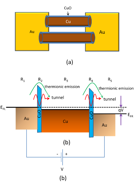
When a potential difference is imposed between the contacts to induce current flow, the energy band diagram in the direction of current flow (along the wire) will appear as shown in Fig. 1(b). Current flows by electrons either tunneling through, or thermionically emitting over, the barriers, or by both mechanisms. The magnitude of the resistance will depend exponentially on the barrier heights (for thermionic emission) [4] or the square-root of the barrier heights (for tunneling) [4]. Any modulation of the barrier heights will therefore cause a large change in a wire’s resistance.
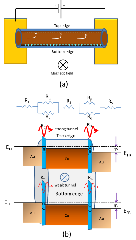
Consider now the situation when a magnetic field is applied transverse to the direction of current flow. The resulting Lorentz force will divert electrons toward one edge of the wire, resulting in electron accumulation at that edge and depletion at the opposite edge as shown in Fig. 2(a). This is the same phenomenon that causes the classical Hall effect. The accumulation of electrons at one edge will pull the barrier down at that edge, whereas the depletion of electrons at the other edge will raise the barrier up at that edge [5]. The sum of the amounts by which the barrier is lowered at one edge and raised at the other is roughly the electronic charge times the Hall voltage that appears between the two edges. Consequently, the energy band diagram at the two edges will look like in Fig. 2(b). Electrons can tunnel (or thermionically emit) much more easily at the top edge than at the bottom edge.
As shown in Fig. 1(b), the resistance of the structure can be thought of as being composed of five resistors in series – the resistance due to the left Au contact, the resistance due to the left barriers (at the accumulated and depleted edges), the resistance due to the Cu wire, the resistance due to the right barriers, and the resistance due to the right Au contact. The dominant resistances are and (since the other resistances are of metallic structures) and these two are modulated by the magnetic field.
Let us carry out a qualitative analysis of how the resistance between the two contacts (at low applied voltage) can change in a magnetic field due to barrier height modulation at the top and bottom edges caused by the deflection of the electron trajectories. Because the analysis is “qualitative”, we will view each of the resistances and as being roughly due to two parallel paths – one along the top edge and the other along the bottom. We will call the resistances of the two barriers at the top edge and , while calling the resistances of the two barriers at the bottom edge and (see Fig. 2(b)). The resistance of the structure can therefore be written as
| (1) | |||||
The resistancs and are determined by tunneling and/or thermionic emission. Let us consider the tunneling case first. Within the WKB approximation, the tunneling transmission probability of an electron impinging on a barrier with energy is [4]
| (2) |
where the -axis is in the direction of current flow, the tunnel barrier extends from to , and is the spatially varying potential energy of the tunnel barrier. Similarly, within the Richardson model, the thermionic emission probability is inversely proportional to the exponential of the (spatially averaged) barrier height at any given temperature [4]. Here, we will analyze the tunneling case. The reader can easily replicate the analysis for the thermionic emission case.
In the tunneling case, the resistance of any barrier is inversely proportional to the tunneling probability. Hence,
| (3) |
where is the resistance and is the (spatially averaged) height of the -th barrier, while is a constant.
Thus, we obtain that in the absence of any magnetic field, the resistance is [from Equations (1) and (3)]
where , , , and .
In the presence of the magnetic field, the tunnel barrier heights decrease by and at the top edge, while increasing by and at the bottom edge (). Therefore,
| (5) |
where
| (6) | |||||
The quantities and depend on the magnetic field and are positive. Although , where is the electronic charge and the Hall voltage that developes between the two edges, we are unable to estimate it quantitatively since the Hall cofficient in the copper nanowires is unknown. That quantity depends on the free electron concentration in the nanowires, which can be several orders of magnitude different from the bulk value owing to defects and surface states that trap electrons.
From Equations (4) - (6), we obtain that
It is interesting to note that if the shrinkage in the barrier height at the top edge is roughly equal to the expansion in the barrier height at the bottom edge, i.e. and , then and . In that case,
It is clear from the above expression that if in the absence of any magnetic field, the top and bottom barriers are similar in height, i.e. , then . In other words, the resistance of the structure will decrease in a magnetic field resulting in negative magnetoresistance.
A similar analysis (algebraically easier) can be carried out for the case of thermionic emission, and the conclusion will be similar.
3 Fabrication
We fabricated 50-nm diameter Cu nanowires by depositing Cu selectively within 50-nm diameter pores of anodic alumina films prepared by anodizing aluminum foils in 0.3M oxalic acid [6]. The thin alumina layer that forms at the bottom of the pores during the anodization process impedes dc current flow along the pores; it was removed by soaking the alumina films in phosphoric acid for 45 - 60 minutes [7]. Next, Cu was selectively electrodeposited within the nanopores from a solution of CuSO4 [8] using a dc current density of 1 mA/cm2. During this step, the sample was immersed in the CuSO4 solution and current was passed through the solution using the aluminum foil as the cathode and a counter electrode as the anode. The Cu++ cations flowed into the pores from the solution because the pores offered the least resistance paths for the dc current. Thus, Cu nanowires of 50 nm diameter formed within the pores of the alumina film. The alumina host was dissolved out in hot chromic/phosphoric acid, leaving the Cu nanowires standing vertically on the aluminum foil. The samples were then ultrasonicated in ethanol to release the wires from the aluminum foil, forming a suspension of Cu nanowires (50 nm diameter and varying length; average length 1 m) in ethanol.
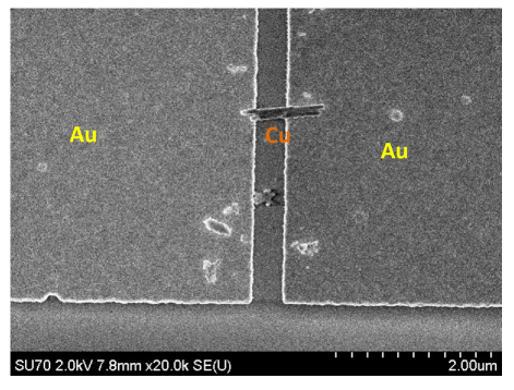
The Cu nanowires in the ethanol suspension were captured across Au contact pads on silicon chips using dielectrophoresis [9, 10, 11]. This involved the following steps. Electron beam lithography was used to create patterns in poly-methyl methacrylate (PMMA) based polymeric resists, which were spin-coated on silicon chips. An 85-nm thick Au film (with a Cr adhesion layer) was deposited on the resist-patterned surface and metal lift-off was performed to create spatially separated nanoelectrode pairs on the chips. Next, the nanowire containing ethanol suspension was pipetted on to the surface of the silicon chip patterned with the Au nanoelectrodes, while applying an ac bias across the nanoelectrodes. This polarized the Cu nanowires in the suspension and exerted a dielectrophoretic (DEP) force that caused them to be captured across the nanoelectrodes. By tuning the excitation voltage (4V, peak-to-peak) and its frequency (1 kHz) over a given deposition period (4 minutes), the DEP region of influence was controlled to extend over suspension volumes that present single or a few nanowires [11]. This resulted in an array of devices on the chip with a single or a few nanowires assembled across the Au nanoelectrodes. From these assembled device arrays, single (or few) nanowire assembly locations were selected for further testing. A scanning electron microscope image of a representative device with two assembled nanowires is shown in Fig. 3.
4 Results
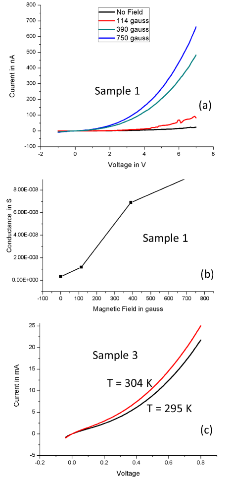
The current voltage characteristics of the nanowires were measured at room temperature with a HP 4156B semiconductor parameter analyzer under different magnetic fields. The plot for one sample is shown in Fig. 4 (a). These plots are repeatable from run to run and do not show any instability,
The characteristics in Fig. 4(a) are expectedly non-linear because of the tunneling through, and/or thermionic emission over, the barriers. The current at a given voltage increases with increasing magnetic field, resulting in a negative magnetoresistance (or positive magnetoconductance). The conductance at a fixed voltage of 7 V is plotted as a function of magnetic field in Fig. 4(b). In our set up, the maximum magnetic field we can apply is 75 mT.
In Fig. 4(c), we show the current-voltage characteristic of a third sample at zero magnetic field measured at two different temperatures. Increased temperature increases the conductance, despite the fact that phonon scattering in copper should incerase when the sample is heated. This increase happens because transport occurs via thermionic emission over a barrier and the emission rate increases with temperature. The increase is however relatively modest which tells us that thermionic emission is not the only modality of transport; there is also significant tunneling through the barrier.
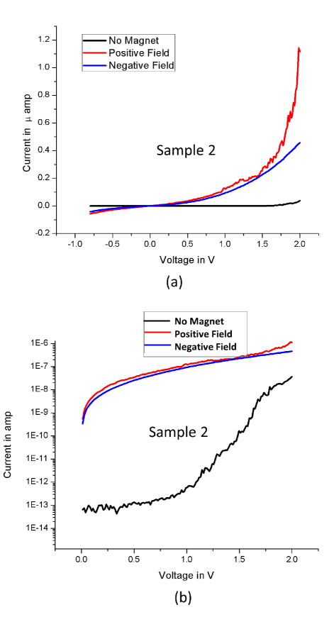
In Fig. 5(a), we show the current-voltage plots for a fixed magnetic field strength of 39 mT, but for two anti-parallel directions of the field. There is a difference between the two cases since the electrons are deflected to opposite edges and the transport characteristics of the two edges are, expectedly, somewhat different. In this case, we have also plotted the current-voltage characteristic in log-linear scale in Fig. 5(b) to show that the magnetoconductance is astoundingly large – the resistance can change by over five orders of magnitude in a magnetic field of 39 mT under an applied voltage of 250 mV (Fig. 5), resulting in a super-giant magnetoresistance of 10,000,000% at that magnetic field. The low voltage makes it an extremely low power device – the maximum power dissipation at that voltage level is 5 nW.
One disconcerting feature is that there is significant variability in the absolute conductance of the samples, as is evident from the current-voltage characteristics of samples 1, 2 and 3. This is obviously due to the fact that the copper oxide film cannot be well controlled and the current is inversely proportional to the exponential of the barrier height for thermionic emission (square-root of barrier height for tunneling). In the tunneling case, the current is also inversely proportional to the exponential of the barrier width, or the oxide film thickness. Because of this variability, some samples do not show the effect while others do. Better control may be achieved by growing the oxide layer with atomic layer deposition, instead of relying on atmospheric oxidation. This is, however, a yield-related concern that does not impute the physics of the effect.
5 Conclusions
In conclusion, we have shown that a giant magnetoconductance can result in a metal nanowire from magnetic field modulation of potential barrier heights at metal-contact interfaces. The field deflects electron trajectories toward one edge of the metal nanowire which causes the local electron concentration at that edge to rise while the concentration at the other edge falls. This lowers the potential barrier height at the first edge and raises it at the second. The effect of this is to alter the nanowire’s conductance and the change in the conductance can be super-giant. This effect is different from the traditional giant magnetoresistance effect accruing from spin-dependent scattering in magnetic multilayers [12, 13], or tunneling magnetoresistance in magnetic tunnel junctions [14], or tunneling of electrons (injected by a ferromagnetic contact) between Landau levels in adjacent graphene layers [15]. It is much larger and can be used in all the traditional applications of giant magnetoresistance, such as in magnetic read heads and magnetic field sensors.
Acknowledgements
This work was supported by the US National Science Foundation under grant CMMI-1301013.
References
- [1] B. Dieny, V. S. Speriosu, S. S. P. Parkin, B. A. Gurney, D. R. Wilhoit and D. Mauri 1991 Phys. Rev. B 43 1297.
- [2] S. S. P. Parkin, C. Kaiser, A. Panchula, P. M. Rice, B. Hughes, M. Samanta and S. H. Yang 2004 Nature Mater. 3 862.
- [3] F. K. Mugwang’a, P. K. Karimi, W. K. Njoroge, O. Omayio and S. M. Waita 2013 Int. J. Thin Film Sci. 2 15.
- [4] S. M. Sze, Physics of Semiconductor Devices, 2nd ed., (John Wiley & Sons, New York, 1981).
- [5] R. F. Pierret, Semiconductor Device Fundamentals, (Addison-Wesley, Reading, Massachusetts, 1996).
- [6] H. Zeng, S. Michalski, R. D. Kirby, D. J. Sellmyer, L. Menon and S. Bandyopadhyay 2002 J. Phys.: Condens. Matter. 14 715.
- [7] S. Bandyopadhyay, Md. I. Hossain, H. Ahmad, J. Atulasimha and S. Bandyopadhyay 2014 Small 10 4379.
- [8] L. Menon, M. Zheng, H. Zeng, S. Bandyopadhyay and D. J. Sellmyer 2000 J. Elec. Mater. 29 510.
- [9] D. Xu, A. Subramanian, L. X. Dong and B. J. Nelson 2009 IEEE Trans. Nanotechnol. 8 449.
- [10] B. R. Burg, V. Bianco, J. Schneider and D. Poulikakos 2010 J. Appl. Phys. 107 14308.
- [11] N. K. R. Palapati, E. Pomerantseva and A. Subramanian 2015 Nanoscale 7 3109.
- [12] M. N. Baibich, J. M. Broto, A. Fert, F. N. Vandau, F. Petroff, P. Eitenne, G. Creuzet, A. Friederich and J. Chazelas 1988 Phys. Rev. Lett. 61 2472.
- [13] G. Binasch, P. Grunberg, F. Saurenbach and W. Zinn 1989 Phys. Rev. B 39 4828.
- [14] S. Ikeda, K. Miura, H. Yamamoto, K. Mizunuma, H. D. Gan, M. Endo, S. Kanai, J. Hayakawa, F. Matsukura and H. Ohno 2010 Nature Mater. 9 721.
- [15] S. C. Bodepudi, A. P. Singh and S. Pramanik 2014 Nano Letters 14 2233.