Scalable gate architecture for densely packed semiconductor spin qubits
Abstract
We demonstrate a 12 quantum dot device fabricated on an undoped Si/SiGe heterostructure as a proof-of-concept for a scalable, linear gate architecture for semiconductor quantum dots. The device consists of 9 quantum dots in a linear array and 3 single quantum dot charge sensors. We show reproducible single quantum dot charging and orbital energies, with standard deviations less than 20% relative to the mean across the 9 dot array. The single quantum dot charge sensors have a charge sensitivity of 8.210 and allow the investigation of real-time charge dynamics. As a demonstration of the versatility of this device, we use single-shot readout to measure a spin relaxation time = 170 ms at a magnetic field = 1 T. By reconfiguring the device, we form two capacitively coupled double quantum dots and extract a mutual charging energy of 200 eV, which indicates that 50 GHz two-qubit gate operation speeds are feasible.
pacs:
03.67.Lx, 73.63.Kv, 85.35.GvI Introduction
The density of transistors in integrated circuits has been following Moore’s law since its conception Moore (1965). However, as the size of transistors approaches the size of a single atom the laws of quantum physics will play an increasingly dominant role in computer architectures, making it difficult for this trend to continue much longer. Despite this, the prospect of utilizing quantum mechanical phenomena in information processing offers an opportunity to increase the computational power of computers, for some types of problems, beyond what is known to be possible on even the most ideal classical computer Shor (1999); Grover (1996). In order for functional quantum computers to become a reality, they will require an on-chip physical component with reproducible properties that can be incorporated into large scale structures, much like the classical computer depends on the robustness of the transistor.
One of the leading candidates for the quantum analog of the transistor is the gate-defined, semiconductor quantum dot Kouwenhoven et al. (1997); Hanson et al. (2007). The spin state of an electron trapped in a quantum dot is an ideal physical system for storing quantum information Loss and DiVincenzo (1998); DiVincenzo et al. (2000); Taylor et al. (2005). Silicon in particular, with its weak hyperfine fields, small spin-orbit coupling and lack of piezoelectric electron-phonon coupling, forms a “semiconductor vacuum” for spin states Steger et al. (2012), and supports seconds-long electron spin coherence times Tyryshkin et al. (2012). However, the fabrication of reliable and scalable Si based quantum dots has proved challenging. Independent of the need for a pure spin environment, quantum dots must have reproducible electrical properties for scaling. The relatively large effective mass of electrons in Si, along with the typically lower mobilities of Si two-dimensional electron gases, makes the fabrication of tightly confined, few-electron quantum dots with reproducible properties difficult Payette et al. (2012).

In this paper we present a path forward for scaling up semiconductor quantum dot devices. Our device consists of 12 quantum dots, 9 of which are arranged in a linear array, and 3 that are used as sensitive charge detectors. The enhancement mode device utilizes an overlapping aluminum gate architecture to achieve tight electronic confinement Zajac et al. (2015), while the undoped Si/SiGe heterostructure provides a clean, high mobility interface Mi et al. (2015) for the formation of well-behaved quantum dots with reproducible characteristics.
II Results and Discussion
The outline of the paper is as follows. We first evaluate the reproducibility of the 9 dots in the array by extracting the critical parameters of single quantum dots formed under each plunger gate: the lever-arm, charging energy and orbital excited state energy. We are able to reach zero electron occupancy in all 9 quantum dots in the array, obtaining an average charging energy = 6.9 0.7 meV and an average orbital energy = 3.0 0.5 meV. Using adjacent single quantum dots as charge sensors, we show that we are able to read out the charge state of the entire array with a signal-to-noise ratio (SNR) that allows for the observation of real-time tunneling events. Lastly, as a demonstration of the flexibility of the gate architecture, we perform single-shot spin readout and demonstrate strong capacitive coupling of two nearest-neighbor double quantum dots (DQDs).
II.1 Linear Gate Architecture
A false-colored SEM image of the device is shown in Fig. 1(a) and a COMSOL simulation of the electron density in the plane of the quantum well is shown in Fig. 1(b). Tight electronic confinement is achieved using an overlapping aluminum gate architecture Zajac et al. (2015). In the upper half of the device, two sets of aluminum gate electrodes, with a pitch of 100 nm, are interleaved to form a linear array of 9 quantum dots. A plunger gate controls the chemical potential of each quantum dot (shown in red), while barrier gates control the tunnel coupling of adjacent dots (shown in green). An aluminum screening layer restricts the action of the tuning gates to a one-dimensional channel Zajac et al. (2015). High sensitivity single electron charge detection is achieved using 3 single dot charge sensors defined in a second one-dimensional channel that is formed in the lower half of the device.
The scalability of this device design is evident from its repeating unit cell structure. Each unit cell consists of 3 quantum dots and a charge sensor. The device demonstrated here is constructed by concatenating 3 of these unit cells. Scaling to arrays of arbitrary length is achievable by adding additional unit cells. The overlapping gate architecture demonstrated here has roughly 4.5 times the areal density of a widely-used DQD depletion mode gate pattern; we fit 9 dots and 3 charge sensors in an area of , the same area as a GaAs DQD and its two quantum point contact charge detectors Petta et al. (2005).
II.2 Characterization of the 9 Dot Array
Scaling to large arrays of quantum dots requires uniform and reliable single quantum dot characteristics. We adopt three figures of merit to characterize the reproducibility of the linear array: the lever-arm , charging energy , and orbital excited state energy . We form a single quantum dot under each plunger gate with the neighboring quantum dots tuned to the many electron regime and extract , and for each dot using a combination of transport measurements, charge sensing, and pulsed gate spectroscopy.
Lever-arms are extracted from transport measurements of Coulomb diamonds at the = 0 to 1 transition, where refers to the number of electrons in the dot. The charge state of each dot is read out by measuring the conductance through the nearest single dot charge sensor. As an example, Fig. 2(a) shows the charge stability diagram of a quantum dot formed under plunger gate P9. Here the derivative of the charge sensor conductance, , is plotted as a function of and . The lack of charge transitions for low values of indicates that dot 9 has been emptied of free electrons, reaching = 0 charge occupancy. Addition voltages for dot 9 are extracted along the vertical dashed line in Fig. 2(a) and converted into addition energies, , using . These addition energies are plotted in Fig. 2(b). For comparison, we also show the addition energies for dots 4, 6, and 8. The increase in at the = 4 to 5 charge transition is attributed to shell filling of the low lying spin and valley degrees of freedom Yang et al. (2013); Borselli et al. (2011).
Pulsed gate spectroscopy is performed in each dot at the = 0 to 1 charge transition to extract the orbital excited state energy Elzerman et al. (2004a); Yang et al. (2012). A 500 Hz square wave with peak-to-peak amplitude is added to the dc plunger gate voltage to repeatedly load and unload an electron onto and off of the dot. For small only the ground state is pulled below the Fermi level of the lead [upper panel in Fig. 2(c)] and an electron tunnels onto the dot with a rate . When the pulse amplitude exceeds , the electron can load into either the ground state or the first excited state [lower panel in Fig. 2(c)]. The effective loading rate is increased due to the contribution from the excited state and is visible in the charge sensing data as a change in the average sensor conductance. From these data we extract an orbital excited state energy = = 3.4 meV for dot 9.
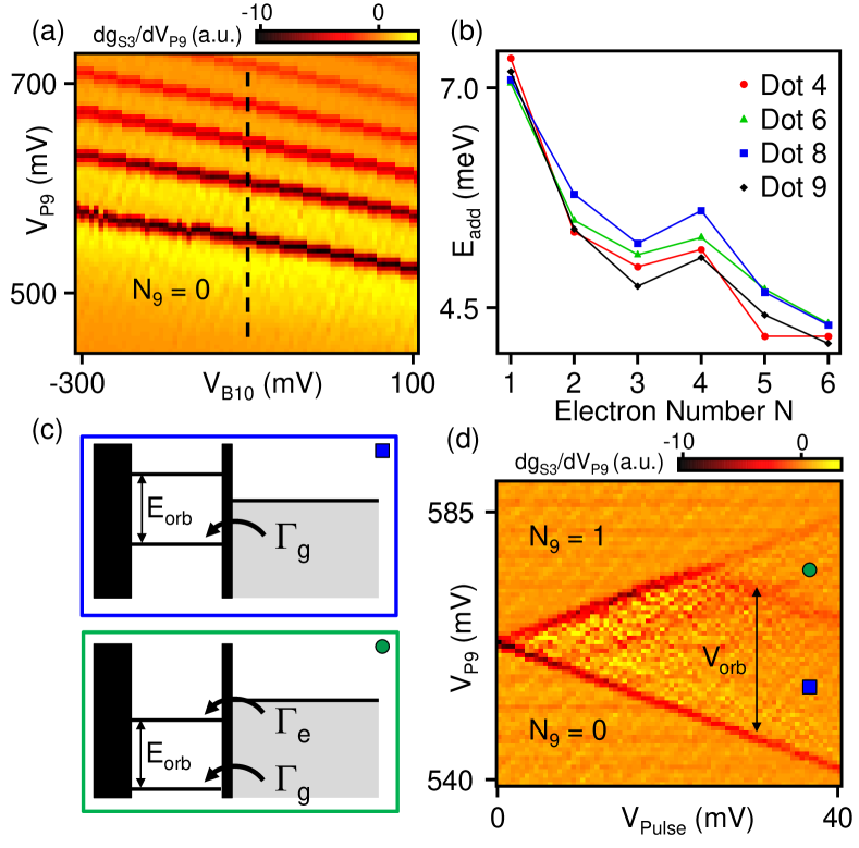
Similar characterization is performed on dots 1–8 and the results are summarized in Table 1. The averaged figures of merit are = 0.13 0.01 meV/mV, = 6.9 0.7 meV, and = 3.0 0.5 meV. These charging energies are generally larger than those obtained with other device designs in Si/SiGe due to the tight confinement potential generated by the overlapping gate architecture. Specifically, depletion mode devices achieved charging energies of less than 2 meV Yuan et al. (2011), while enhancement mode architectures have yielded charging energies close to 5 meV Borselli et al. (2011). Moreover, the large orbital excited state energies are comparable to those measured in GaAs devices, where the effective mass is nearly three times smaller than Si Hanson et al. (2007).
| Dot | (meV/mV) | E (meV) | E (meV) |
|---|---|---|---|
| 1 | 0.14 | 6.6 | 2.7 |
| 2 | 0.13 | 6.1 | 2.6 |
| 3 | 0.11 | 5.6 | 2.1 |
| 4 | 0.14 | 7.3 | 3.3 |
| 5 | 0.14 | 7.2 | 3.3 |
| 6 | 0.14 | 7.1 | 3.0 |
| 7 | 0.14 | 7.7 | 3.5 |
| 8 | 0.14 | 7.1 | 3.4 |
| 9 | 0.13 | 7.2 | 3.4 |
II.3 Sensitive Charge Detection
An important criterion for quantum information processing is high fidelity qubit readout. For both single-shot readout of an individual spin Elzerman et al. (2004b); Morello et al. (2010) and spin-to-charge conversion in double Petta et al. (2005) and triple quantum dot qubits Medford et al. (2013a) this translates to a need for high fidelity charge state readout. We demonstrate high sensitivity charge detection using the charge sensor array. The 3 sensor dots give good coverage over the entire 9 dot array.
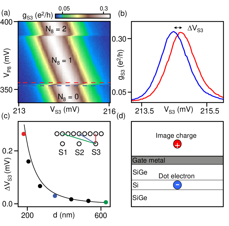
In order to characterize the charge sensor performance we first measure the shift in a charge sensor Coulomb blockade peak due to a change in the charge occupancy of a nearby dot in the linear array. As an example, in Fig. 3(a), we plot the conductance through charge sensor 3, , as a function of and . A Coulomb blockade peak is visible in the sensor dot conductance and it abruptly shifts each time an electron is added to quantum dot 8. We measure a peak shift of = 0.26 mV at the = 0 to 1 charge transition. The shift in the charge sensor 3 Coulomb blockade peak position is also measured for dots 2–7 and is plotted in Fig. 3(c) as a function of the geometric distance, , between each dot and the sensor dot. The shift falls off with a power law that is close to .
Predictions for the shifts in the sensor dot Coulomb blockade peak position can be obtained by computing the capacitances of the device. We construct a 3-dimensional model of the device based on the wafer growth profile and lithographic gate dimensions, representing the dots as metallic cylinders with a radius of 19 nm and height of 5 nm, each centered 7 nm below the Si/SiGe interface. The capacitances of the device are then computed using the fast-multipole-moment solver FastCap fas . The expected shift is computed from the simulated capacitances using where is the mutual capacitance between the sensor dot and the single-electron dot, is the capacitance between the sensor dot and its plunger gate, and is the total single-electron dot capacitance Van der Wiel et al. (2002). The computed shift scales as and agrees nicely with the experimental data [see the solid black line in Fig. 3(c)]. We point out that the accuracy of this model is limited by uncertainty in the exact location of the quantum dots in the quantum well.
As in the case of a parallel plate capacitor, one might expect the capacitance to scale as 1/. However, the overlapping gate architecture covers nearly the entire Si/SiGe heterostructure with metal, resulting in a significant amount of screening. The impact of this screening can be understood using the method of images charges [Fig. 3(d)]. An electron trapped in a quantum dot induces a positive image charge in the gate metal above. The resulting electric field due to the electron and its image charge is that of a dipole, which falls off with a 1/ dependence.
II.4 Real-Time Charge Detection
The ability to resolve real-time charge dynamics allows the study of fundamental physical phenomena at the level of single electrons Küng et al. (2012); Maisi et al. (2016). It also enables single-shot readout of single electron spin states Elzerman et al. (2004b); Morello et al. (2010) and the discrimination of two-electron singlet and triplet spin states Petta et al. (2005). We now demonstrate high sensitivity charge detection through the observation of real-time tunneling events Vandersypen et al. (2004); Gustavsson et al. (2009). Through a quantitative analysis of the charge sensor response, we extract a charge sensitivity of 8.210.
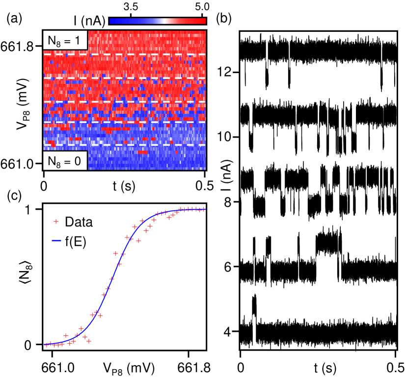
Figure 4(a) shows a color-scale plot of the current through sensor dot 3 as a function of time, for a range of plunger gate voltages with dot 8 tuned up near the = 0 to 1 charge transition. Five time series extracted from this data set are plotted in Fig. 4(b). The lowest time-series in Fig. 4(b) was acquired with = 661.12 mV. Here the dot is empty nearly all of the time. With slightly increased, the current shows signatures of real-time single electron tunneling events and switches between two levels corresponding to the = 0 and 1 charge states. As expected, the dwell time in the = 1 charge state increases with increasing . Using a threshold to discriminate between the charge states, we plot the time-averaged occupation of dot 8, , as a function of in Fig. 4(c). We expect the population to follow a Fermi function as the chemical potential of the dot level is lowered past the Fermi level of the lead. The data in Fig. 4(c) are nicely fit to a Fermi function with an electron temperature = 120 mK.
A detailed analysis of the real-time single electron tunneling events can be used to determine the charge sensor SNR and charge sensitivity. We first measure a one-second time series of the current through the charge sensor with dot 8 tuned to the = 0 to 1 charge degeneracy point. The data are acquired at a sampling rate of 500 kHz and a Kaiser-Bessel finite impulse response (FIR) filter is used to reduce the effective measurement bandwidth to 30 kHz, the 3 dB point of our room temperature amplifier. A 30 ms long segment of this time series is shown in Fig. 5(a). Real-time tunneling events between = 0 and = 1 are seen as two level switching in the measured current. A histogram of the full time trace is shown in Fig. 5(b). The two well-resolved peaks correspond to the two charge states. Each peak is nicely fit to a Gaussian with width = 0.112 nA, corresponding to the current noise in our measurement setup. The centroids of the two Gaussians are separated by = 0.772 nA, which corresponds to the signal associated with a change in electron occupancy of one. For these data we extract a SNR = / = 6.9. By adjusting the FIR filter cutoff frequency, , we plot the SNR as a function of the effective measurement bandwidth in Fig. 5(c), showing a decrease in the SNR with increasing .
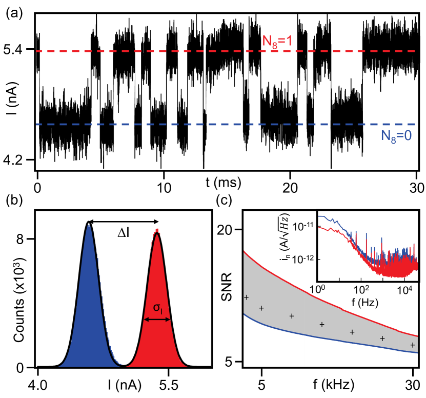
A quantitative description of the SNR requires a more careful analysis of the experimental setup. We therefore measure the current noise of the device. The measured noise spectra, , at current levels of 4 nA (6 nA) are plotted as the blue (red) traces in the inset of Fig. 5(c). The noise is approximately white at high frequencies, but noise with an approximate dependence dominates at low frequency, and the overall noise level appears to be correlated to the derivative of the charge sensor current with respect to gate voltage. We can use these spectra to calculate the expected noise for a one second time series by integrating over frequency from 1 Hz to the filter cutoff frequency, :
| (1) |
Using the measured signal = 0.772 nA, we plot the expected SNR as a function of in Fig. 5(c). The measured SNR falls within the shaded region between the two curves that delineate the expected SNR for current levels of 4 and 6 nA. For a 30 kHz bandwidth the SNR = 6.9, implying an effective charge sensitivity of 8.210. This sensitivity is higher than both the rf-QPC ( ) Reilly et al. (2007) and dispersive gate readout (6.3 ) Colless et al. (2013), however our measurement bandwidth is limited to 30 kHz due to our current amplifier. Improvements to the SNR and measurement bandwidth could be made by using a low temperature preamplifier Curry et al. (2015) in combination with a higher bandwidth room temperature amplifier.
II.5 Versatility Demonstrations
The 9 dot linear array is capable of hosting a diverse range of quantum dot qubits. Using individual spins, 9 nearest-neighbor exchange coupled Loss-DiVincenzo qubits can be formed within the array Loss and DiVincenzo (1998). With the gate voltages configured differently, four singlet-triplet qubits could be formed using pairs of electrons Petta et al. (2005) and the qubits could be coupled via a dipole-dipole interaction Shulman et al. (2012). Alternatively, three exchange-only spin qubits could be defined, allowing full electrical control over the Bloch sphere of each qubit Medford et al. (2013a, b); Eng et al. (2015). To demonstrate the versatility of this device architecture we first perform single-shot readout of an electron spin to measure the spin lifetime, . Finally, we form two capacitively coupled DQDs and measure an interaction strength of 200 eV, which suggests a 50 GHz two-qubit gate operation speed.
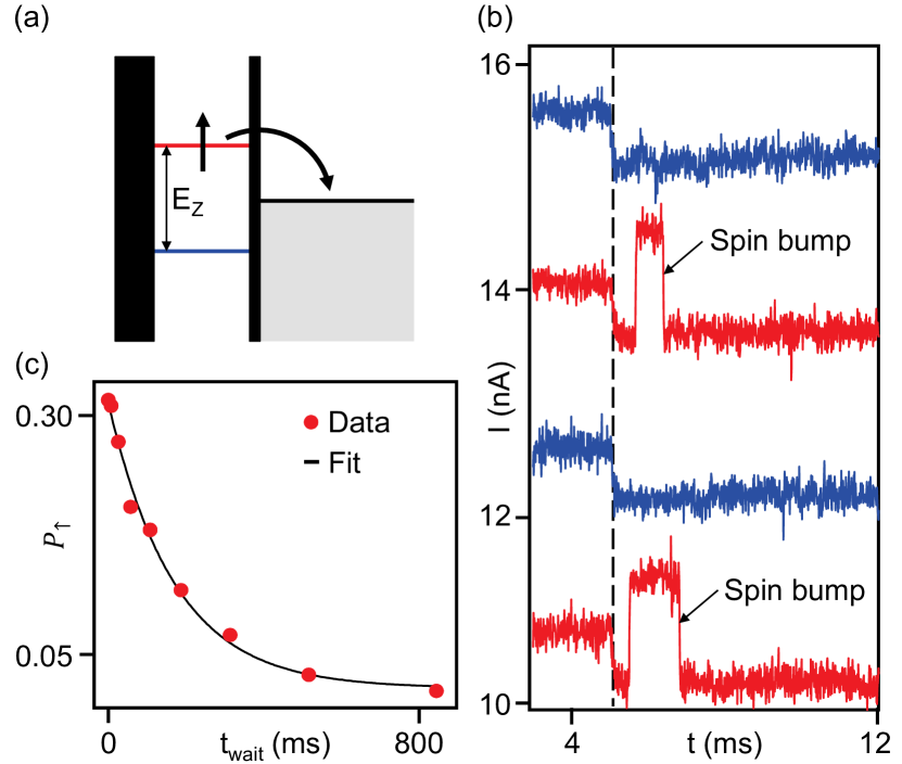
We now demonstrate single-shot spin state readout on dot 8 in the linear array. A three-step pulse sequence is employed to measure the spin relaxation time at a magnetic field = 1 T Elzerman et al. (2004b); Morello et al. (2010). Starting with an empty dot, we plunge the chemical potential of the dot level far below the Fermi level of the lead, which allows an electron to load into either the spin up or the spin down state. After a time we begin the readout phase by setting the chemical potential of the dot such that the spin up and spin down energy levels straddle the Fermi level of the lead. If the electron on the dot is in the spin-up excited state, as shown in Fig. 6(a), the electron will hop off of the dot and then be replaced by a spin-down electron. The change in the charge occupancy of the quantum dot due to this process is visible in time series measurements of the sensor dot current, , and is referred to here as a “spin bump.” In contrast, if the final spin state is spin down, no spin bump will be observed. Lastly, we raise the chemical potential of both spin states above the Fermi level to empty the dot and complete the measurement cycle.
Example single-shot traces are shown in Fig. 6(b). Spin up electrons are indicated by current pulses during the readout phase (red traces) while spin down electrons simply remain on the dot during the readout phase (blue traces). We extract by varying and measuring the probability of being in the spin up state at the end of the measurement phase [see Fig. 6(c)]. Each data point represents the average of 10,000 single-shot traces. The resulting data are fit to an exponential decay with a best fit = 170 17 ms. The long spin relaxation time is a defining feature of the Si “semiconductor vacuum.”
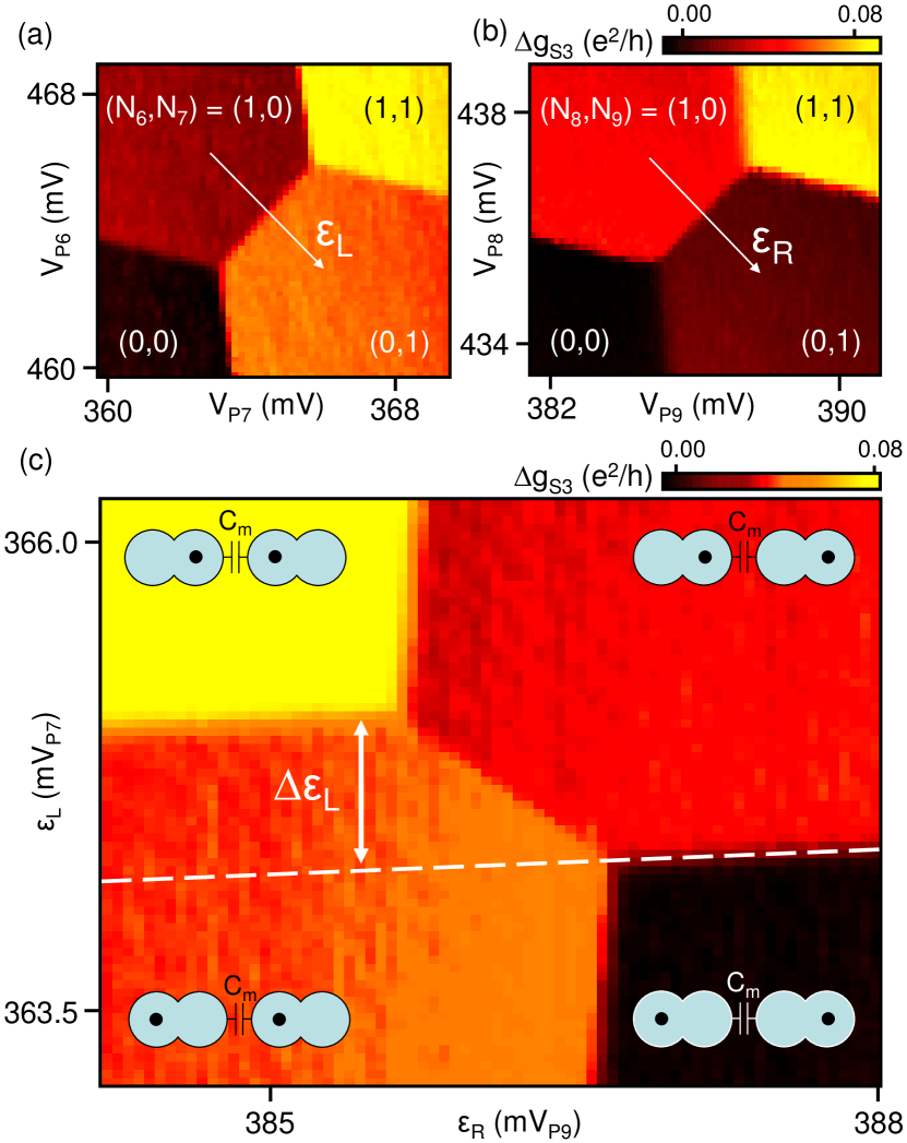
Capacitive coupling has been proposed to mediate two-qubit interactions Taylor et al. (2005). Our compact gate design leads to large capacitive couplings. As a demonstration, we investigate the capacitive coupling of two adjacent DQDs. We use dots 6–7 to define one DQD and dots 8–9 to define a second DQD. The charge stability diagrams for these DQDs are shown in Figs. 7(a–b). The barrier gate voltage is set such that there is no tunneling between dots 7 and 8. As a result, the two DQDs are coupled only via a capacitive interaction . Interdot detuning axes, and , are overlaid on the data in Figs. 7(a–b). By sweeping vs , we obtain the quadruple quantum dot stability diagram shown in Fig. 7(c). The mutual capacitance causes the (, ) = (1,0) to (0,1) interdot charge transition to shift by = 0.77 mV when the occupancy of the second DQD changes from (, ) = (1,0) to (0,1). Using the lever-arm conversion between gate voltage and energy, this corresponds to a 200 eV energy shift (50 GHz two-qubit gate operation time) Ward et al. .
III Conclusion
In summary, we have developed a scalable quantum dot gate architecture that yields quantum dots with uniform and reproducible characteristics. As a proof-of-concept, we have presented a 12 quantum dot device consisting of a linear array of 9 quantum dots and 3 single quantum dot charge sensors. From characterization measurements we obtain standard deviations in the charging energies and orbital energies of less than 20% relative to their means: = 6.9 0.7 meV, = 3.0 0.5 meV. We have demonstrated the ability to detect real-time tunneling events in this large array, and used this capability for single-shot measurements of the electron spin. As a final demonstration, we characterize the dipole-dipole coupling of two adjacent DQDs formed in the array and measure an interaction energy of 200 eV, which bodes well for computing architectures that rely on capacitive coupling of qubits.
IV Acknowledgments
Funded by the ARO through grant No. W911NF-15-1-0149, the Gordon and Betty Moore Foundation’s EPiQS Initiative through Grant GBMF4535, and the NSF (DMR-1409556 and DMR-1420541). Devices were fabricated in the Princeton University Quantum Device Nanofabrication Laboratory.
References
- Moore (1965) G. E. Moore, Cramming more components onto integrated circuits, Electronics 38, 8 (1965).
- Shor (1999) P. W. Shor, Polynomial-time algorithms for prime factorization and discrete logarithms on a quantum computer, SIAM Review 41, 303 (1999).
- Grover (1996) L. K. Grover, in Proceedings of the 28th Annual ACM Symposium on Theory of Computing (ACM, 1996) pp. 212–219.
- Kouwenhoven et al. (1997) L. P. Kouwenhoven, C. M. Marcus, P. L. McEuen, S. Tarucha, R. M. Westervelt, and N. S. Wingreen, Mesoscopic electron transport (Springer, 1997).
- Hanson et al. (2007) R. Hanson, L. P. Kouwenhoven, J. R. Petta, S. Tarucha, and L. M. K. Vandersypen, Spins in few-electron quantum dots, Rev. Mod. Phys. 79, 1217 (2007).
- Loss and DiVincenzo (1998) D. Loss and D. P. DiVincenzo, Quantum computation with quantum dots, Phys. Rev. A 57, 120 (1998).
- DiVincenzo et al. (2000) D. P. DiVincenzo, D. Bacon, J. Kempe, G. Burkard, and K. B. Whaley, Universal quantum computation with the exchange interaction, Nature (London) 408, 339 (2000).
- Taylor et al. (2005) J. M. Taylor, H.-A. Engel, W. Dür, A. Yacoby, C. M. Marcus, P. Zoller, and M. D. Lukin, Fault-tolerant architecture for quantum computation using electrically controlled semiconductor spins, Nat. Phys. 1, 177 (2005).
- Steger et al. (2012) M. Steger, K. Saeedi, M. L. W. Thewalt, J. J. L. Morton, H. Riemann, N. V. Abrosimov, P. Becker, and H.-J. Pohl, Quantum Information Storage for Over 180 s Using Donor Spins in a 28Si “Semiconductor Vacuum,” Science 336, 1280 (2012).
- Tyryshkin et al. (2012) A. M. Tyryshkin, S. Tojo, J. J. L. Morton, H. Riemann, N. V. Abrosimov, P. Becker, H.-J. Pohl, T. Schenkel, M. L. W. Thewalt, K. M. Itoh, et al., Electron spin coherence exceeding seconds in high-purity silicon, Nat. Mater. 11, 143 (2012).
- Payette et al. (2012) C. Payette, K. Wang, P. J. Koppinen, Y. Dovzhenko, J. C. Sturm, and J. R. Petta, Single charge sensing and transport in double quantum dots fabricated from commercially grown Si/SiGe heterostructures, Appl. Phys. Lett. 100, 043508 (2012).
- Zajac et al. (2015) D. M. Zajac, T. M. Hazard, X. Mi, K. Wang, and J. R. Petta, A reconfigurable gate architecture for Si/SiGe quantum dots, Appl. Phys. Lett. 106, 223507 (2015).
- Mi et al. (2015) X. Mi, T. M. Hazard, C. Payette, K. Wang, D. M. Zajac, J. V. Cady, and J. R. Petta, Magnetotransport studies of mobility limiting mechanisms in undoped Si/SiGe heterostructures, Phys. Rev. B 92, 035304 (2015).
- Petta et al. (2005) J. R. Petta, A. C. Johnson, J. M. Taylor, E. A. Laird, A. Yacoby, M. D. Lukin, C. M. Marcus, M. P. Hanson, and A. C. Gossard, Coherent Manipulation of Coupled Electron Spins in Semiconductor Quantum Dots, Science 309, 2180 (2005).
- Yang et al. (2013) C. H. Yang, A. Rossi, R. Ruskov, N. S. Lai, F. A. Mohiyaddin, S. Lee, C. Tahan, G. Klimeck, A. Morello, and A. S. Dzurak, Spin-valley lifetimes in a silicon quantum dot with tunable valley splitting, Nat. Commun. 4, 2069 (2013).
- Borselli et al. (2011) M. G. Borselli, R. S. Ross, A. A. Kiselev, E. T. Croke, K. S. Holabird, P. W. Deelman, L. D. Warren, I. Alvarado-Rodriguez, I. Milosavljevic, F. C. Ku, et al., Measurement of valley splitting in high-symmetry Si/SiGe quantum dots, Appl. Phys. Lett. 98, 123118 (2011).
- Elzerman et al. (2004a) J. M. Elzerman, R. Hanson, L. H. W. Van Beveren, L. M. K. Vandersypen, and L. P. Kouwenhoven, Excited-state spectroscopy on a nearly closed quantum dot via charge detection, Appl. Phys. Lett. 84, 4617 (2004a).
- Yang et al. (2012) C. H. Yang, W. H. Lim, N. S. Lai, A. Rossi, A. Morello, and A. S. Dzurak, Orbital and valley state spectra of a few-electron silicon quantum dot, Phys. Rev. B 86, 115319 (2012).
- Yuan et al. (2011) M. Yuan, F. Pan, Z. Yang, T. J. Gilheart, F. Chen, D. E. Savage, M. G. Lagally, M. A. Eriksson, and A. J. Rimberg, Si/SiGe quantum dot with superconducting single-electron transistor charge sensor, Appl. Phys. Lett. 98, 142104 (2011).
- Elzerman et al. (2004b) J. M. Elzerman, R. Hanson, L. H. W. Van Beveren, B. Witkamp, L. M. K. Vandersypen, and L. P. Kouwenhoven, Single-shot read-out of an individual electron spin in a quantum dot, Nature (London) 430, 431 (2004b).
- Morello et al. (2010) A. Morello, J. J. Pla, F. A. Zwanenburg, K. W. Chan, K. Y. Tan, H. Huebl, M. Möttönen, C. D. Nugroho, C. Yang, J. A. van Donkelaar, et al., Single-shot readout of an electron spin in silicon, Nature (London) 467, 687 (2010).
- Medford et al. (2013a) J. Medford, J. Beil, J. M. Taylor, E. I. Rashba, H. Lu, A. C. Gossard, and C. M. Marcus, Quantum-dot-based resonant exchange qubit, Phys. Rev. Lett. 111, 050501 (2013a).
- (23) FastCap (http://www.fastfieldsolvers.com/).
- Van der Wiel et al. (2002) W. G. Van der Wiel, S. De Franceschi, J. M. Elzerman, T. Fujisawa, S. Tarucha, and L. P. Kouwenhoven, Electron transport through double quantum dots, Rev. Mod. Phys. 75, 1 (2002).
- Küng et al. (2012) B. Küng, C. Rössler, M. Beck, M. Marthaler, D. S. Golubev, Y. Utsumi, T. Ihn, and K. Ensslin, Irreversibility on the level of single-electron tunneling, Phys. Rev. X 2, 011001 (2012).
- Maisi et al. (2016) V. F. Maisi, A. Hofmann, M. Röösli, J. Basset, C. Reichl, W. Wegscheider, T. Ihn, and K. Ensslin, Spin-Orbit Coupling at the Level of a Single Electron, Phys. Rev. Lett. 116, 136803 (2016).
- Vandersypen et al. (2004) L. M. K. Vandersypen, J. M. Elzerman, R. N. Schouten, L. H. W. Van Beveren, R. Hanson, and L. P. Kouwenhoven, Real-time detection of single-electron tunneling using a quantum point contact, Appl. Phys. Lett. 85, 4394 (2004).
- Gustavsson et al. (2009) S. Gustavsson, R. Leturcq, M. Studer, I. Shorubalko, T. Ihn, K. Ensslin, D. C. Driscoll, and A. C. Gossard, Electron counting in quantum dots, Surf. Sci. Rep. 64, 191 (2009).
- Reilly et al. (2007) D. J. Reilly, C. M. Marcus, M. P. Hanson, and A. C. Gossard, Fast single-charge sensing with a rf quantum point contact, Appl. Phys. Lett. 91, 162101 (2007).
- Colless et al. (2013) J. I. Colless, A. C. Mahoney, J. M. Hornibrook, A. C. Doherty, H. Lu, A. C. Gossard, and D. J. Reilly, Dispersive readout of a few-electron double quantum dot with fast rf gate sensors, Phys. Rev. Lett. 110, 046805 (2013).
- Curry et al. (2015) M. J. Curry, T. D. England, N. C. Bishop, G. Ten-Eyck, J. R. Wendt, T. Pluym, M. P. Lilly, S. M. Carr, and M. S. Carroll, Cryogenic preamplification of a single-electron-transistor using a silicon-germanium heterojunction-bipolar-transistor, Appl. Phys. Lett. 106, 203505 (2015).
- Shulman et al. (2012) M. D. Shulman, O. E. Dial, S. P. Harvey, H. Bluhm, V. Umansky, and A. Yacoby, Demonstration of entanglement of electrostatically coupled singlet-triplet qubits, Science 336, 202 (2012).
- Medford et al. (2013b) J. Medford, J. Beil, J. M. Taylor, S. D. Bartlett, A. C. Doherty, E. I. Rashba, D. P. DiVincenzo, H. Lu, A. C. Gossard, and C. M. Marcus, Self-consistent measurement and state tomography of an exchange-only spin qubit, Nat. Nanotechnol. 8, 654 (2013b).
- Eng et al. (2015) K. Eng, T. D. Ladd, A. Smith, M. G. Borselli, A. A. Kiselev, B. H. Fong, K. S. Holabird, T. M. Hazard, B. Huang, P. W. Deelman, et al., Isotopically enhanced triple-quantum-dot qubit, Science Advances 1, e1500214 (2015).
- (35) D. R. Ward, D. Kim, D. E. Savage, M. G. Lagally, R. H. Foote, M. Friesen, S. N. Coppersmith, and M. A. Eriksson, State-conditional coherent charge qubit oscillations in a Si/SiGe quadruple quantum dot, arXiv:1604.07956 .